
Optimization of Reversible Circuits Using Toffoli Decompositions with Negative Controls


1
Department of Mathematics and Computer Science, Faculty of Science, Alexandria University, Alexandria 21568, Egypt
2
Academy of Scientific Research and Technology(ASRT), Cairo 11516, Egypt
3
School of Computer Science, University of Birmingham, Birmingham B15 2TT, UK
*
Author to whom correspondence should be addressed.
Symmetry 2021, 13(6), 1025; https://doi.org/10.3390/sym13061025
Submission received: 2 May 2021
/
Revised: 28 May 2021
/
Accepted: 1 June 2021
/
Published: 7 June 2021
(This article belongs to the Section Computer)
Abstract
:The synthesis and optimization of quantum circuits are essential for the construction of quantum computers. This paper proposes two methods to reduce the quantum cost of 3-bit reversible circuits. The first method utilizes basic building blocks of gate pairs using different Toffoli decompositions. These gate pairs are used to reconstruct the quantum circuits where further optimization rules will be applied to synthesize the optimized circuit. The second method suggests using a new universal library, which provides better quantum cost when compared with previous work in both cost015 and cost115 metrics; this proposed new universal library “Negative NCT” uses gates that operate on the target qubit only when the control qubit’s state is zero. A combination of the proposed basic building blocks of pairs of gates and the proposed Negative NCT library is used in this work for synthesis and optimization, where the Negative NCT library showed better quantum cost after optimization compared with the NCT library despite having the same circuit size. The reversible circuits over three bits form a permutation group of size 40,320 , which is a subset of the symmetric group, where the NCT library is considered as the generators of the permutation group.
1. Introduction
One of the problems in classical computers is heat dissipation and energy loss. The amount of energy dissipated for any lost bit of information is calculated by R. Landauer’s principle, which is , where K is the Boltzmann’s constant ( JK−1) and T is the temperature of the system. Reversible computing has one of many features, where no heat dissipation is produced by the system [1]; hence, no information is destroyed. This feature has many applications [2], such as low-power CMOS [3], nanotechnology [4], DNA-based logic circuit with self error recovery capability employing massive parallelism [5] and many more [6].
Quantum computing is reversible by nature [7]. Recently, using group theory in studying the reversible logic synthesis problem has gained attention [8,9]. Group theory is also used to find a relationship between the decomposition of a reversible circuit and a quantum circuit in [10]. A relationship between the reversible logic synthesis problem and Young subgroups is introduced in [11]. A reversible gate is the basic building block of a reversible circuit [3]. Quantum gates are reversible gates/functions, which are considered as a special case of symmetry groups of finite spaces (Young subgroups) [10]. Many methods have been proposed to optimize the quantum cost of circuits [12,13]. The quantum cost of the NCT library is reduced in [14]; a further reduction of the quantum cost of the NCT library is made in [15]. The algorithms in [16,17] use an ancillary qubit to achieve less quantum cost. Universal reversible gate libraries are proposed in [18,19,20], which use GAP-based algorithms to synthesize reversible circuits using different types of gates with various gate costs. Different Toffoli decompositions are proposed in [21] to reduce the quantum cost of reversible circuits. Toffoli gates have control qubits, which can be positive or negative. The positive control is applied if the system is in the excited state, whereas the negative control is applied if the system is in the ground state. The importance of the ground state over the excited state in systems for better stability is discussed in [22], which shows that systems tend to be more stable in the ground state compared with the excited state, so using negative controls is more stable and has less quantum cost for the system compared with using positive controls [23,24,25,26].
The paper has two aims: the first aim of this paper is to propose an algorithm that optimizes the quantum cost of 3-bit reversible circuits based on a modified version of the NCT library; the second aim is to propose a new gate library by modifying the NCT library to replace positive control with negative control, which shows less quantum cost compared with the NCT library.
This paper is organized as follows: Section 2 gives a brief introduction to elementary quantum gates used to build quantum circuits, permutation group, definitions and terminologies used in this paper. Section 3 introduces the proposed library and proposed synthesis algorithm. Section 4 shows the experimental results. The paper concludes in Section 5.
2. Background
This section gives a brief introduction on the basics of reversible circuit, Negative NCT library gates and permutation group.
2.1. Reversible Boolean Function
A Boolean function f with n inputs and n outputs is considered to be reversible if and only if each input vector is mapped to a unique output vector where . For n inputs there are different reversible Boolean functions, for there is = 40,320 3-input/output reversible Boolean functions.
Given a finite set , is permutation and a bijection function that maps an input to an output from A such that , it can be represented as a permutation as follows in (1).
The top row is ordered so that it can be eliminated, so can be written as in (2).
The permutation can also be represented as a product of disjoint cycles. For example, can be written as .
2.2. Reversible Quantum Logic
Quantum computers use qubit as the basic unit of information, which is represented by a state vector. The vector: represents a single qubit where and are complex numbers that satisfy the condition . The measurement of determines the state of the system. Four states of the system are used in this paper; the first state is the standard state where is 0, the second state is the standard state where is 0, the third state is where and the fourth state is where .
2.3. Reversible Gates
A reversible gate is a reversible Boolean function in which each input vector has a unique output vector.
2.3.1. One-Qubit Gates
This section introduces the one qubit reversible gates that are used in this paper.
NOT gate (N): A reversible gate that maps to and vice versa, also maps to and vice versa. The superscript of N gate is 3 when N gate is applied on a three-qubit reversible circuit () and the subscript of N gate refers to a specific qubit that NOT gate is applied on. For example, applies a NOT gate on the second qubit in a three-qubit reversible circuit. Table 1 shows the effect of a NOT gate on one qubit.
There are three possible gates of a NOT gate for three-qubit reversible circuits as shown in Figure 1a with the following permutations in (3):
Square-root of NOT gate (v): A reversible gate that maps to , to , to , and to .
Square-root of NOT gate (): A reversible gate that maps to , to , to and to .
2.3.2. Condition on Control Qubits
Controlled gates that operate on two or more qubits have at least one control qubit. The condition on control qubit(s) must be satisfied in order for the gate to operate on the target qubit.
Definition 1.
The condition on a control qubit is a condition that must be satisfied so that the gate on the target qubit is applied. The condition on the control qubit could be negative or positive.
If the condition on the control qubit is negative or positive, then the gate on the target qubit will be applied if the control qubit’s state is or , respectively [27]. For example, a gate that has n control qubits with a negative condition on the control qubits will operate on the target qubit if all of the control qubits’ states are . In this paper, the negative control is represented in figures by ∘ and the positive control is represented by •. Only negative control gates are used in this paper because the quantum systems are more stable in the ground state, where the negative control gates are used compared with the excited state in which the positive control gates are applied [22,23,24,25,26].
2.3.3. Two-Qubit Gates
These gates operate on two qubits in which one qubit is the control qubit and the other qubit is the target qubit.
Controlled NOT gate(CNOT/C): A two-qubit gate, which has two versions: positive CNOT (CNOT) and negative CNOT (OCNOT).
In the CNOT gate and OCNOT gate, if the control qubit’s state is and , respectively, then negation will be applied on the target qubit, while the control qubit’s state remains unchanged; otherwise it does nothing.
The superscript of the C gate is 3 when the CNOT/OCNOT gate is applied on a three-qubit reversible circuit (). The subscript of gate consists of two adjacent numbers, the number on the left-hand side represents the control qubit and the number on the right-hand side represents the target qubit. For example, represents the CNOT gate with a positive control on the first qubit and a target on the second qubit; represents the OCNOT gate with a negative control on the first qubit and a target on the second qubit.
The truth table of the CNOT gate is shown in Table 1. There are six possible gates for the CNOT gate for three-qubit reversible circuits as shown in Figure 1b. The truth table of the OCNOT gate is shown in Table 1. There are six possible gates of the OCNOT gate for three-qubit reversible circuits as shown in Figure 1c with the following permutations in (4):
Controlled-V: A two-qubit gate that has two versions: positive V () and negative V (). In the gate and gate, if the control qubit’s state is and , respectively, then the v gate is applied to the target qubit and the control qubit’s state remains unchanged; otherwise it does nothing.
Controlled-: A two-qubit gate that has two versions: positive () and negative (). In the gate and gate, if the control qubit’s state is and , respectively, then the gate is applied to the target qubit and the control qubit’s state remains unchanged; otherwise it does nothing.
2.3.4. Three-Qubit Gate
These gates operate on three qubits, where two qubits are the control qubits and the third qubit is the target qubit.
Controlled controlled NOT (CCNOT) or (Toffoli/T gate):
In this paper, we use two different versions of the Toffoli gate: positive Toffoli (Toffoli) and negative Toffoli (OToffoli). In the Toffoli gate and OToffoli gate, if the control qubits’ states are and , respectively, then the negation will be applied on the target qubit, while the control qubits’ states remain unchanged; otherwise it does nothing. Mixed Control Toffoli gates also exist where one of the control qubits is negative and the other control qubit is positive.
The superscript of T gate is 3 when the Toffoli/OToffoli gate is applied on a three-qubit reversible circuit (). The subscript of gate consists of three adjacent numbers: the first two numbers starting from the left-hand side indicate the control qubits and the number on the right-hand side indicates the target qubit. For example, represents the Toffoli gate with positive control qubits. represents the OToffoli gate with negative control qubits. and represent the Mixed Control Toffoli gates with mixed control qubits.
There are three possible gates for a Toffoli gate for three-qubit reversible circuits as shown in Figure 1f. There are three possible gates for an OToffoli gate for three-qubit reversible circuits as shown in Figure 1g. Some examples of Mixed Control Toffoli gates are shown in Figure 1h. The truth table for the Toffoli and OToffoli gates are shown in Table 1. The following OToffoli permutations are introduced in (5):
2.3.5. Quantum Cost of a Reversible Circuit
The quantum cost of a reversible circuit, which is denoted by Q.C in this paper is the count of the one-qubit and the two-qubit elementary gates in the decomposition of the circuit.
In this paper, two methods for calculating the quantum cost are used: the cost015 metric [28] and cost115 metric [29]. In the cost015 metric: the quantum cost of a one-qubit gate is 0, two-qubit gate is 1 and three-qubit gate is 5 [30]. In the cost115 metric: the quantum cost of a one-qubit gate is 1, two-qubit gate is 1 and three-qubit gate is 5.
2.3.6. Optimization Rules of Quantum Gates: Moving, Merging and Splitting
For a three-qubit quantum circuit with a set of wires , where the first qubit is 1, the second qubit is 2 and the third qubit is 3. Let be any two-qubit gate whose control qubit is negative on qubit 1 and its target qubit is on qubit 2, where .
Table 2 shows the moving rules where a gate can be swapped with its adjacent gate. For example, the one-qubit NOT gate that acts on the first qubit can be swapped with its adjacent one-qubit gate that acts on any of the other two qubits; the gate can also be swapped with its adjacent two-qubit gate if the control qubit in the two-qubit gate is not the same as the qubit that acts on; in this case can be swapped with , , , , , , , ,, , and . Adjacent two-qubit gates can be swapped if they have the same control qubit or if they have the same target qubit. For example, can be swapped with , , , , and .
Table 3 shows the merging rules in which two adjacent gates can be merged to form a new gate. For example, any two adjacent one-qubit gates that are applied on the same qubit can be merged to form an identity gate if the application of the second gate reverses the first gate. Any two adjacent two-qubit gates with the same control qubit and the same target qubit can form a new gate. For example, are merged to form . Furthermore, if two adjacent two-qubit gates in which the control qubit of the first gate is the same as the target qubit of its adjacent gate, and the target qubit of the first gate is the same as the control qubit in its adjacent gate, then these gates can form a new gate and the resulting two-qubit gate has a quantum cost of 1 in both of the cost015 and cost115 metrics [15]. For example, can be merged to form a two-qubit gate . In this paper, the visual representation of this gate is shown by surrounding this two-qubit gate with a dashed box and its quantum cost is 1 [15]. The splitting rules are the reverse of the merging rules, these optimization rules are used in [14,15,16,17,18,21].
3. The Proposed Negative NCT-Gate Library
This section explains the proposed Negative NCT gate library for building three-qubit reversible circuits. The Negative NCT gate library that works on three-qubit reversible circuits consists of three types of gates: one-qubit gates, two-qubit gates and three-qubit gates. This proposed library consists of 12 gates and their detailed information is represented in Section 2. The 12 gates are three NOT gates, six OCNOT gates and three OToffoli gates. An implementation of the Schreier–Sims algorithm on the GAP software is used to generate the set of all possible three-qubit reversible circuits with the least length (40,319 circuits excluding the identity [20]), which shows the universality of the Negative NCT gate library for 3-bit reversible circuits.
3.1. Gate Decomposition
Definition 2.
Gate symbol is a unique symbol that refers to a gate where is an integer number. For example, and . Table 4 shows the gates with their corresponding gate symbol (sym.).
The decomposition of a gate is a set of elementary gates that can be used to synthesize a quantum circuit equivalent to this gate, each set of these elementary gates is given a number d starting from 0. For example, represents the gate symbol in its 0th decomposition. One-qubit gates and two-qubit gates are elementary gates themselves; hence, each gate has only one decomposition denoted by the 0th decomposition, which is the gate itself.
Table 5 shows the Negative NCT gates with their corresponding decomposition(s) where each one-qubit gate or two-qubit gate has only one decomposition, which is the gate itself, while each three-qubit gate can be decomposed using (NOT, CNOT, V, ) gates, which was shown to be optimal [30]. The three-qubit gate has eight different decompositions. Figure 2, Figure 3 and Figure 4 show the eight different decompositions for each OToffoli gate that depend on the Toffoli decompositions in [21]. This paper uses only negative control decompositions, while [21] uses only positive control decompositions.
Right and Left Gate Sets of a Decomposition
Definition 3.
The ordered pair of a gate () is an ordered pair that contains the control qubit and the target qubit of a gate .
An example of an for a three-qubit system is , where the control is on the first qubit and the target is on the third qubit. , , , , and are some examples of gates in which their is .
Definition 4.
The sets and of a circuit are the sets that contain the of the right-hand side gate and left-hand side gate, respectively.
The set or the set contains ordered pairs with the same control qubit or the same target qubit; otherwise the set or the set contains one element only. An example of the set of gate in Figure 2a is , where the two ordered pairs in the set have the same control qubit in this example and the set of gate is . Another example of the set of gate in Figure 3b is and the set of gate is , where the two ordered pairs in the set have the same target qubit in this example.
Each decomposition of the OToffoli gates contains two gate sets; the set and the set where each of these sets contains elements, the of a gate is concerned with the control qubit and the target qubit only, and it does not concern with the condition on the control qubit nor the functionality of the gate itself. The set and the set of a decomposition contain the of the gate on the right-hand side and the left-hand side, respectively. For example, decomposition, which is shown in Figure 2a has a left-hand side gate, which is , where the control qubit is on qubit 2 (the second qubit) and the target qubit is on qubit 3 (the third qubit), so this gate’s is (2,3); hence, the set of is , if gate and its next gate can be swapped, then the of the next gate can also be added to the set; cannot be swapped with ; hence, the set for this decomposition remains unchanged. The right-hand side gate in decomposition is where this gate’s is (1,3); hence, the set of is if the gate and its prior gate can be swapped then the of gate’s prior gate can be added to the set; can be swapped with ; hence, the set is updated to .
In two-qubit gates, the set = the set = the of the gate.
Table 6 shows the Negative NCT gates that have corresponding and sets.
3.2. Basic Pairs
Definition 5.
A basic pair is a circuit that consists of two consecutive decomposed gates with minimal quantum cost and lower decomposition number.
The set of all possible circuits that represent a pair of gates is calculated by multiplying the count of decompositions of each gate inside this pair. For example, the pair begins with the gate, which has eight different decompositions as shown in Figure 2, and the second gate is the gate, which has eight different decompositions as shown in Figure 3, so there are 64 different circuits for this pair of gates. Section 3.2.1 shows a technique that chooses the circuit with the least quantum cost out of these 64 different circuits in order to represent the basic pair for this pair of gates .
3.2.1. Choosing the Basic Pair
Definition 6.
The sets and of a circuit are the sets of all and sets, respectively.
Two adjacent gates with the same control and target qubits can be combined to form a new gate according to the merging rules in Table 3. Therefore, the technique to choose the circuit with minimal cost works through finding the largest set that results from the intersection of the set of the first gate with the set of the second gate inside the basic pair, if the two sets are mutually exclusive, then it finds the largest set that results from intersecting the invert of the set of the first gate with the set of the next gate. For example, if the set of the first gate includes , and there are no mutual elements in the set of the next gate, then it searches for in the set of the second gate instead, since these two gates can form a two-qubit gate with a quantum cost of 1 according to the merging rules in [15].
For example, the pair has 64 different circuits to represent it. The basic pair with the least quantum cost of this pair is in which the decomposition number of the first gate is 0 and the decomposition number of the next gate is 1 since the intersection of the set of and the set of is according to Table 6, then the final quantum cost of this basic pair is 7 instead of 10. Figure 5 shows the basic pair where Figure 5a shows the basic pair before optimization with a quantum cost of 10, the gate on the right-hand side of and the gate on the left-hand side of are marked with arrows. Figure 5b shows the basic pair after swapping the marked gates, then the gates in the solid boxes are prepared for merging. Figure 5c shows the basic pair after applying the merging rules and forming two two-qubit gates, then the newly formed two-qubit gate on the left hand-side is marked. Figure 5d shows the basic pair after moving the marked gate to the right-hand side and marking the other resulting two-qubit gate. Figure 5e shows the basic pair after moving the marked gate to the left-hand side and finally applying further optimization, where the quantum cost is reduced to 7 after forming a two-qubit gate with a quantum cost of 1 [15].
Another example is , where is a two-qubit gate, then it has only one decomposition , choosing or will reduce the quantum cost of this basic pair to 4 instead of 6, where the of the gate matches the of the gate, while choosing , , or will reduce the quantum cost to 5 after optimization. Finally, choosing or will not reduce the quantum cost at all, a visual explanation of this example is shown in Figure 6, where and have the least quantum cost but the basic pair of circuit is since the basic pair with lower decomposition number () is considered to be the basic pair for this pair as shown in Table 7.
The Negative NCT library consists of 12 gates and the total number of basic pairs (which have the lowest quantum cost) for this library is basic pairs. Table 7 shows the Negative NCT library’s basic pairs excluding basic pairs that contain NOT gates and basic pairs in which both gates are OCNOT gates because there is no further reduction.
Table 7 also shows the quantum cost of the basic pair before and after optimization and its corresponding circuit.
3.2.2. Build a Circuit with Basic Pairs
Definition 7.
The of a gate is the gate in its 0th decomposition.
Basic pairs are concatenated to form circuits, the of the basic pair and the of the next basic pair are called a “point of connection”. For example, the circuit consists of four gates, each two gates starting from the left-hand side are replaced with their corresponding basic pair, so in this case the circuit consists of two basic pairs where the first basic pair is and the next basic pair is as shown in Figure 7.
Let S be the total number of gates in a circuit; whether, S is even or odd determines the number of basic pairs and , which are used to build the circuit, where the number of in a circuit is ≤2. Two methods are going to be proposed in the next sections in order to choose the basic pairs to reconstruct a circuit.
3.3. Circuit Optimization Algorithm
Definition 8.
The basic pair solitary () quantum cost is the summation of all quantum costs of all basic pairs and , which are used to build the circuit.
FunctionI (Algorithm 1) is used by the proposed circuit optimization algorithm (Algorithm 2) to reconstruct each circuit of the three-qubit system by using basic pairs of gates. In FunctionI (Algorithm 1), the gates are paired starting from the left-hand side gate of the circuit. represents the corresponding basic pairs of the ith and ith + 1 gates in the circuit C, if S is odd, then the last gate on the right-hand side of the circuit is merged with the circuit as a where decomposes the OToffoli gate in its 0th decomposition and returns other gates unchanged. Finally, applies optimization rules on the points of connection of the circuit.
| Algorithm 1 FunctionI (C) |
| function |
| ifS = 1 |
| then return (C) |
| else if S ≠ 1 |
| then for i ← 0 to S/2 |
| ifS mod 2 = 1 |
| then O+ = Solitary(CS) |
| O = optimize(O) |
| return (O) |
| Algorithm 2 Circuit Optimization (ONCT) |
| procedure |
| for eachC ∈ ONCT |
| do C = FunctionI(C) − |
For example, the circuit has a quantum cost of 17 and is translated to , and this circuit consists of five gates (where ), the reconstructed circuit is paired from the left-hand side into two pairs and maintaining the order of pairs from left to right; these pairs are replaced with their corresponding basic pairs; with a quantum cost of 4 and with a quantum cost of 7 according to Table 7, the gate on the right-hand side is and it will be decomposed into its decomposition number 0 since S is odd, where has a quantum cost of 1, the quantum cost of this reconstructed circuit is 12 instead of 17 in the cost015 metric, the optimization rules are then applied on points of connection of the reconstructed circuit and the final quantum cost for this reconstructed circuit is 11. Figure 8 shows the decomposition steps of the circuit before and after applying the optimization rules. The dashed box in Figure 8 refers to a two-qubit gate with a quantum cost of 1 [15].
3.4. Modified Circuit Optimization Algorithm
In Algorithm 2, the optimization technique depends on FunctionI (Algorithm 1). FunctionII (Algorithm 3) splits the circuit into basic pairs starting from the second gate on the left-hand side instead of the first gate. If S is odd and , then the circuit is reconstructed as a and basic pairs(s), while for even , then the circuit is reconstructed as a then basic pair(s) and finally a . For example, the circuit has a quantum cost of 11, which can be reconstructed using FunctionI (Algorithm 1) which results in two basic pairs and one on the right-hand side: with a quantum cost of 5, with a quantum cost of 5 and with a quantum cost of 0, the quantum cost for this circuit using FunctionI (Algorithm 1) is 10; using FunctionII (Algorithm 3) gives one on the left-hand side and two basic pairs: with a quantum cost of 0, with a quantum cost of 7 and with a quantum cost of 1, where the quantum cost for this circuit using FunctionII (Algorithm 3) is 8, the latter function shows a better quantum cost for this circuit and the final quantum cost using FunctionII (Algorithm 3) is 7 after applying the optimization rules on the points of connection instead of 11 in the cost015 metric as shown in Figure 9.
Figure 9 illustrates the circuit example before and after applying the optimization rules in the cost015 metric, the dashed box indicates forming a two-qubit gate with a quantum cost of 1 [15].
| Algorithm 3 FunctionII (C) |
| function |
| ifS = 1 |
| then return (C) |
| else if S = 2 |
| else if S > 2 |
| ifS mod 2 = 0 |
| then O+ = Solitary(CS) |
| O = optimize(O) |
| return (O) |
IBM Quantum Experience system [31] was used to implement the circuit, whose permutation was . The system has five qubits, a Canary r2 processor, with an average CNOT error of , and average readout error of . The IBM Quantum Experience does not currently support the gate where qubit qubit b, so this gate is replaced with gates since they are equivalent according to the splitting rules, which are the reverse of the merging rules in Table 3. The IBM Quantum Experience does not also support the negative control qubit, so the positive control qubit is used and NOT gates are added before and after each positive control qubit in the quantum circuit as shown in Figure 10 since they are equivalent according to [32].
The reconstructed circuit , which is obtained from applying FunctionII (Algorithm 3) is modified to be compatible with the system by applying the splitting rules and the rule in Figure 10. The implementation of the circuit on the system has a quantum cost of 7 as shown in Figure 11, while the implementation of the equivalent quantum circuit, whose permutation is using the NCT library has a quantum cost of 11 as shown in Figure 12.
Some circuits have less quantum cost if they are reconstructed using FunctionI (Algorithm 1), other circuits have less quantum cost if FunctionII (Algorithm 3) is used to reconstruct them.
The modified circuit optimization algorithm (Algorithm 4) calculates the quantum cost for each circuit using of FunctionI (Algorithm 1) and FunctionII (Algorithm 3), then it chooses the function, which has less quantum cost in order to reconstruct the quantum circuit, where m represents a mark to the function having less quantum cost.
| Algorithm 4 Modified Circuit Optimization (ONCT) |
| procedure |
| for eachC ∈ ONCT |
For example, the circuit, which is equivalent to the permutation has a quantum cost of 8. The quantum cost for the circuit using FunctionI (Algorithm 1) is 6 and the quantum cost using FunctionII (Algorithm 3) is 7, so Algorithm 4 chooses FunctionI (Algorithm 1) to decompose the circuit, where the circuit is reconstructed using two basic pairs, which are with a quantum cost of 5, followed by with a quantum cost of 1 according to [15]. The circuit is shown in Figure 13 before optimization, after optimization, and the equivalent circuit on the system after using the splitting rules and the preparation of negative gates as shown in Figure 10. While the implementation of the equivalent quantum circuit, whose permutation is using the NCT library on the system has a quantum cost of 15 as shown in Figure 14.
From the examples in Figure 13 and Figure 14, it is shown that the Negative NCT library has less quantum cost for this example compared with the NCT library. Extending the Negative NCT library for n-qubits, where n is achievable since higher order gates can be decomposed into three-qubit gates according to [30,33].
4. Experimental Results
This section describes the experiments on three-qubit reversible circuits based on the proposed Negative NCT library and compares the results with relevant libraries in [15,16,17,18,19]. The Negative NCT library shows an average length as in the NCT library, which equals . The comparison includes the proposed circuit optimization algorithm (Algorithm 2) and the proposed modified circuit optimization algorithm (Algorithm 4).
Table 8 compares the average quantum cost of three-qubit reversible circuits in the cost015 metric using the proposed Negative NCT library and the works found in the literature, where the average quantum cost of the Negative NCT library after using the proposed modified circuit optimization algorithm (Algorithm 4) is , while the average quantum cost of the Negative NCT library using the proposed circuit optimization algorithm (Algorithm 2) is . Finally, the quantum cost of the Negative NCT library before optimization is . Table 8 compares the obtained results with other libraries in [15,18,19], where the average quantum cost after optimization is in [15], in [18] and in [19].
Table 9 compares the average quantum cost of three-qubit reversible circuits in cost115 metric using the proposed Negative NCT library after applying the proposed optimization algorithms (Algorithms 2 and 4) with the works found in the literature. Table 9 shows the average quantum cost of the Negative NCT library after applying the proposed modified circuit optimization algorithm (Algorithm 4) is , while the average quantum cost of the Negative NCT library after applying the proposed circuit optimization algorithm (Algorithm 2) is . The average quantum cost of the NCT library using the optimization algorithm in [15] is .
There is an inverse proportional relationship between the quantum cost and the number of ancillary qubits that are used by an algorithm to optimize a quantum circuit. The quantum cost obtained [17] is in cost115 metric, which is less than the proposed method in this paper because this method uses a single ancillary qubit, while Algorithm 4 is applied without using any ancillary qubits.
The proposed approach uses negative control gates, which is more stable because it depends on the ground state of the quantum system, which will help in building real quantum computers because one of the biggest challenges in building practical quantum computers is the decoherence and the instability of the quantum system. Furthermore, the proposed algorithm produces low-cost quantum circuits, which will help in building stable medium scale and small scale quantum computers because it will help in making the computation perform faster to overcome the decoherence of the quantum system over a long period of time.
5. Conclusions
This paper proposed two algorithms (The circuit optimization algorithm and the modified circuit optimization algorithm), both of which use basic pairs as building blocks to reconstruct the circuit, choosing between the two proposed pairing functions (FunctionI and FunctionII) depending on the nature of the circuit; both show better results compared to reconstructing the circuit with a fixed pairing function regardless of the nature of the circuit as in the modified circuit optimization algorithm and the circuit optimization algorithm, respectively. The modified circuit optimization algorithm is applied to the Negative NCT library with an average quantum cost of in cost115 metric and in cost015 metric without using any ancillary qubits.
The paper also proposed optimization methods for the quantum cost of the three-qubit reversible circuit using Negative NCT library. The proposed method was compared with related optimization methods from the literature and the comparisons show that the average minimum cost of the proposed Negative NCT library is in the cost015 metric and in the cost115 metric, which is less than NT, NCT, NR3, and NM3 libraries. The comparison showed that using Negative NCT library instead of NCT library gives less quantum cost, which equals .
The proposed algorithms work with universal libraries that use a set or a subset of NOT, OCNOT, and OToffoli gates. This work can be extended by finding other pairing functions for each circuit in the Negative NCT library to minimize the quantum cost. Another extension is to apply the proposed algorithms on different universal libraries.
Author Contributions
Conceptualization, M.G. and A.Y.; supervision, A.Y.; software M.G.; validation M.G. and A.Y.; writing the paper, M.G. and A.Y. All authors have read and agreed to the published version of the manuscript.
Funding
This project was supported financially by the Academy of Scientific Research and Technology (ASRT), Egypt, Grant No 6565, (ASRT) is the 2nd affiliation of this research.
Institutional Review Board Statement
Not applicable.
Informed Consent Statement
Not applicable.
Data Availability Statement
Not applicable.
Acknowledgments
We acknowledge the use of IBM Quantum services for this work. The views expressed are those of the authors, and do not reflect the official policy or position of IBM or the IBM Quantum team.
Conflicts of Interest
The authors declare that they have no conflict of interest.
References
- Landauer, R. Irreversibility and Heat Generation in the Computing Process. IBM J. Res. Dev. 1961, 5, 183–191. [Google Scholar] [CrossRef]
- Nielsen, M.A.; Chuang, I.L. (Eds.) Quantum Computation and Quantum Information; Cambridge University Press: Cambridge, UK, 2011; pp. 604–605. [Google Scholar]
- De Vos, A.; Raa, B.; Storme, L. Generating the group of reversible logic gates. J. Phys. A Math. Gen. 2002, 35, 7063–7078. [Google Scholar] [CrossRef] [Green Version]
- Haghparast, M.; Shams, M.; Navi, K. Novel Reversible Multiplier Circuit in Nanotechnology. World Appl. Sci. J. 2008, 5, 806–810. [Google Scholar]
- Sarker, A.; Ahmed, T.; Rashid, S.M.M.; Anwar, S.; Jaman, L.; Tara, N.; Alam, M.M.; Babu, H.M.H. Realization of reversible logic in DNA computing. In Proceedings of the 2011 11th IEEE International Conference on Bioinformatics and Bioengineering (BIBE 2011), Taichung, Taiwan, 24–26 October 2011; pp. 261–265. [Google Scholar]
- Mamataj, S.; Saha, D.; Banu, N. A review of reversible gates and its application in logic design. Am. J. Eng. Res. 2014, 3, 151–161. [Google Scholar]
- Green, A.S.; Altenkirch, T. From Reversible to Irreversible Computations. Electron. Notes Theor. Comput. Sci. 2008, 210, 65–74. [Google Scholar] [CrossRef] [Green Version]
- Zakablukov, D.V. Application of Permutation Group Theory in Reversible Logic Synthesis. In International Conference on Reversible Computation; Springer: Cham, Switzerland, 2015; pp. 1–15. [Google Scholar]
- Yang, G.; Xie, F.; Hung, W.N.N.; Song, X.; Perkowski, M.A. Realization and synthesis of reversible functions. Theor. Comput. Sci. 2011, 5, 1606–1613. [Google Scholar] [CrossRef] [Green Version]
- De Vos, A.; De Baerdemacker, S. Symmetry groups for the decomposition of reversible computers, quantum computers, and computers in between. Symmetry 2011, 3, 305–324. [Google Scholar] [CrossRef]
- Chattopadhyay, A.; Baksi, A. Reversible Logic Circuit Complexity Analysis via Functional Decomposition. arXiv 2016, arXiv:1602.00101v2. [Google Scholar]
- He, X.; Guan, Z.; Ding, F. The Mapping and Optimization Method of Quantum Circuits for Clifford + T Gate. J. Appl. Math. Phys. 2019, 7, 2796–2810. [Google Scholar] [CrossRef] [Green Version]
- Selim, M. Quantum Cost Optimization for Reversible Sequential Circuit. Int. J. Adv. Comput. Sci. Appl. 2013, 4, 15–21. [Google Scholar] [CrossRef] [Green Version]
- Osman, M. Integration of Irreversible Gates in Reversible Circuits Using NCT Library. IOSR J. Comput. Eng. 2013, 14, 69–79. [Google Scholar] [CrossRef]
- Montaser, R.; Younes, A.; Abdel-Aty, M. Improving the quantum cost of NCT-based reversible circuit. Quantum Inf. Process. 2015, 14, 1249–1263. [Google Scholar] [CrossRef]
- Miller, D.M.; Dueck, G.W. Translation Techniques for Reversible Circuit Synthesis with Positive and Negative Controls. In Recent Findings in Boolean Techniques; Drechsler, R., Grosse, D., Eds.; Springer: Cham, Switzerland, 2021. [Google Scholar]
- Sasanian, Z.; Miller, D.M. NCV realization of MCT gates with mixed controls. In Proceedings of the 2011 IEEE Pacific Rim Conference on Communications, Computers and Signal Processing, Victoria, BC, Canada, 23–26 August 2011; pp. 567–571. [Google Scholar] [CrossRef]
- Montaser, R.; Younes, A.; Abdel-Aty, M. New Design of Universal Reversible Gate Library. Quantum Matter 2017, 6, 89–96. [Google Scholar] [CrossRef]
- Osman, M.; Younes, A.; Ismail, G.; Farouk, R. An Improved Design of n-Bit Universal Reversible Gate Library. Int. J. Theor. Phys. 2019, 58, 2531–2549. [Google Scholar] [CrossRef]
- Younes, A. On the universality of n-bit reversible gate libraries. Appl. Math. Inf. Sci. 2015, 9, 2579–2588. [Google Scholar]
- Ali, M.B.; Hirayama, T.; Yamanaka, K.; Nishitani, Y. Quantum cost reduction of reversible circuits using new toffoli decomposition techniques. In Proceedings of the 2015 International Conference on Computational Science and Computational Intelligence (CSCI 2015), Las Vegas, CA, USA, 7–9 December 2016; Volume 9, pp. 59–64. [Google Scholar]
- Puthoff, H.E. Quantum ground states as equilibrium particle–vacuum interaction states. Quantum Stud. Math. Found. 2016, 3, 5–10. [Google Scholar] [CrossRef] [Green Version]
- Moraga, C. Using negated control signals in Quantum Computing Circuits. Facta Univ. Ser. Electron. Energetics 2011, 24. [Google Scholar] [CrossRef]
- Moraga, C. Mixed polarity reversible Peres gates. Electron. Lett. 2014, 50, 987–989. [Google Scholar] [CrossRef] [Green Version]
- Rahman, M.Z.; Rice, J.E. Templates for Positive and Negative Control Toffoli Networks. In Reversible Computation. RC 2014. Lecture Notes in Computer Science; Yamashita, S., Minato, S., Eds.; Springer: Cham, Switzerland, 2014; Volume 8507. [Google Scholar]
- Soeken, M.; Kirkedal Thomsen, M. White Dots do Matter: Rewriting Reversible Logic Circuits. In Proceedings of the 5th International Conference on Reversible Computation, Victoria, BC, Canada, 4–5 July 2013; pp. 196–208. [Google Scholar]
- Cheng, X.; Guan, Z.; Wang, W.; Zhu, L. A simplification algorithm for reversible logic network of positive/negative control gates. In Proceedings of the 2012 9th International Conference on Fuzzy Systems and Knowledge Discovery (FSKD 2012), Chongqing, China, 29–31 May 2012; pp. 2442–2446. [Google Scholar]
- Storme, L.; De Vos, A.; Jacobs, G. Group theoretical aspects of reversible logic gates. J. Univers. Comput. Sci. 1999, 5, 307–321. [Google Scholar]
- Maslov, D.; Miller, D.M. Comparison of the Cost Metrics for Reversible and Quantum Logic Synthesis. IET Comput. Digit. Tech. 2007, 1, 98–104. [Google Scholar] [CrossRef] [Green Version]
- Barenco, A.; Bennett, C.H.; Cleve, R.; Divincenzo, D.P.; Margolus, N.; Shor, P.; Sleator, T.; Smolin, J.A.; Weinfurter, H. Elementary gates for quantum computation. Phys. Rev. A 1995, 52, 3457–3467. [Google Scholar] [CrossRef] [PubMed] [Green Version]
- IBM Quantum Team. ibmq_ourense v1.0.2. Available online: https://quantum-computing.ibm.com (accessed on 18 December 2020).
- Arabzadeh, M.; Saeedi, M.; Zamani, M.S. Rule-based optimization of reversible circuits. In Proceedings of the Asia and South Pacific Design Automation Conference (ASP-DAC), Taipei, Taiwan, 18–21 January 2010; pp. 849–854. [Google Scholar]
- He, Y.; Luo, M.-X.; Zhang, E.; Wang, H.-K.; Wang, X.-F. Decompositions of n-qubit Toffoli Gates with Linear Circuit Complexity. Int. J. Theor. Phys. 2017, 56, 2350–2361. [Google Scholar] [CrossRef]
Short Biography of Authors
 | Mariam Gado is a MSc. student of computer science at Alexandria University, Egypt. She obtained her BSc. degree in computer science (Special Degree) from Alexandria University, Egypt in 2016. She is a member of Alexandria Quantum Computing Group (AleQCG). She is currently a teaching assistant at Egypt-Japan University of Science and Technology (E-JUST), she was a research assistant and laboratory engineer at E-JUST University from 2017 to 2020. |
 | Ahmed Younes is a Professor of Computer Science at Alexandria University and Honorary Research Fellow at School of Computer Science, University of Birmingham, United Kingdom. He is the founder and leader of Alexandria Quantum Computing Group (AleQCG). He obtained his PhD from University of Birmingham, United Kingdom in 2004. He introduced a new technique, now known as ‘Partial Diffusion Operator’ in the field of amplitude amplification and made a contribution in representing Quantum Boolean circuits as Reed-Muller logic. He published many papers in Quantum Algorithms, Quantum cryptography and Reversible Circuits. |
Figure 1.
The possible gates for three-qubit reversible circuits.

Figure 2.
Decompositions (Decomp.) of where in (a) the first control qubit is on qubit 1 and the second control qubit is on qubit 2, and in (b) the first control qubit is on qubit 2 and the second control qubit is on qubit 1. These decompositions are the negative decompositions, which are based on the positive decompositions in [21].
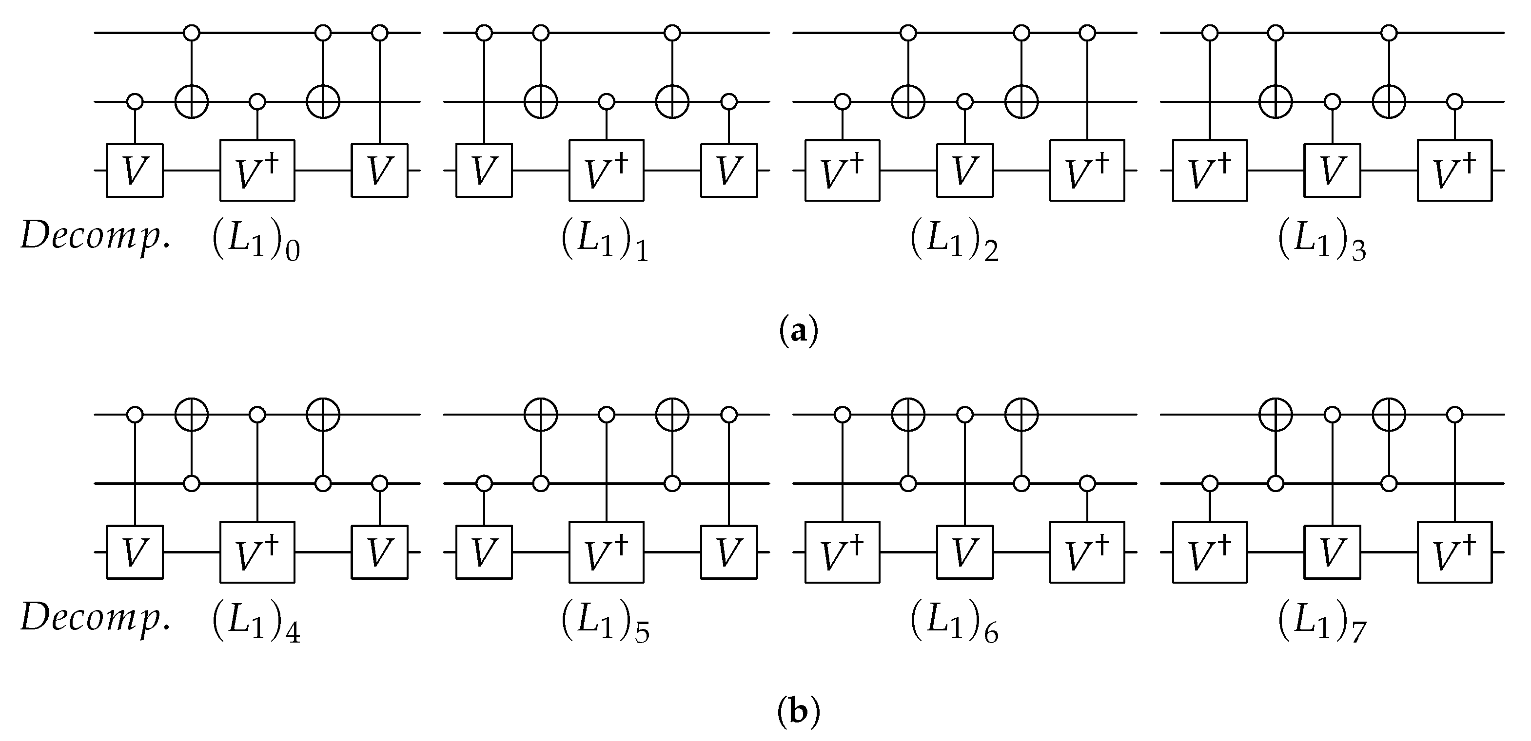
Figure 3.
Decompositions (Decomp.) of where in (a) the first control qubit is on qubit 1 and the second control qubit is on qubit 3, and in (b) the first control qubit is on qubit 3 and the second control qubit is on qubit 1. These decompositions are the negative decompositions, which are based on the positive decompositions in [21].

Figure 4.
Decompositions (Decomp.) of where in (a) the first control qubit is on qubit 2 and the second control qubit is on qubit 3, and in (b) the first control qubit is on qubit 3 and the second control qubit is on qubit 2. These decompositions are the negative decompositions, which are based on the positive decompositions in [21].
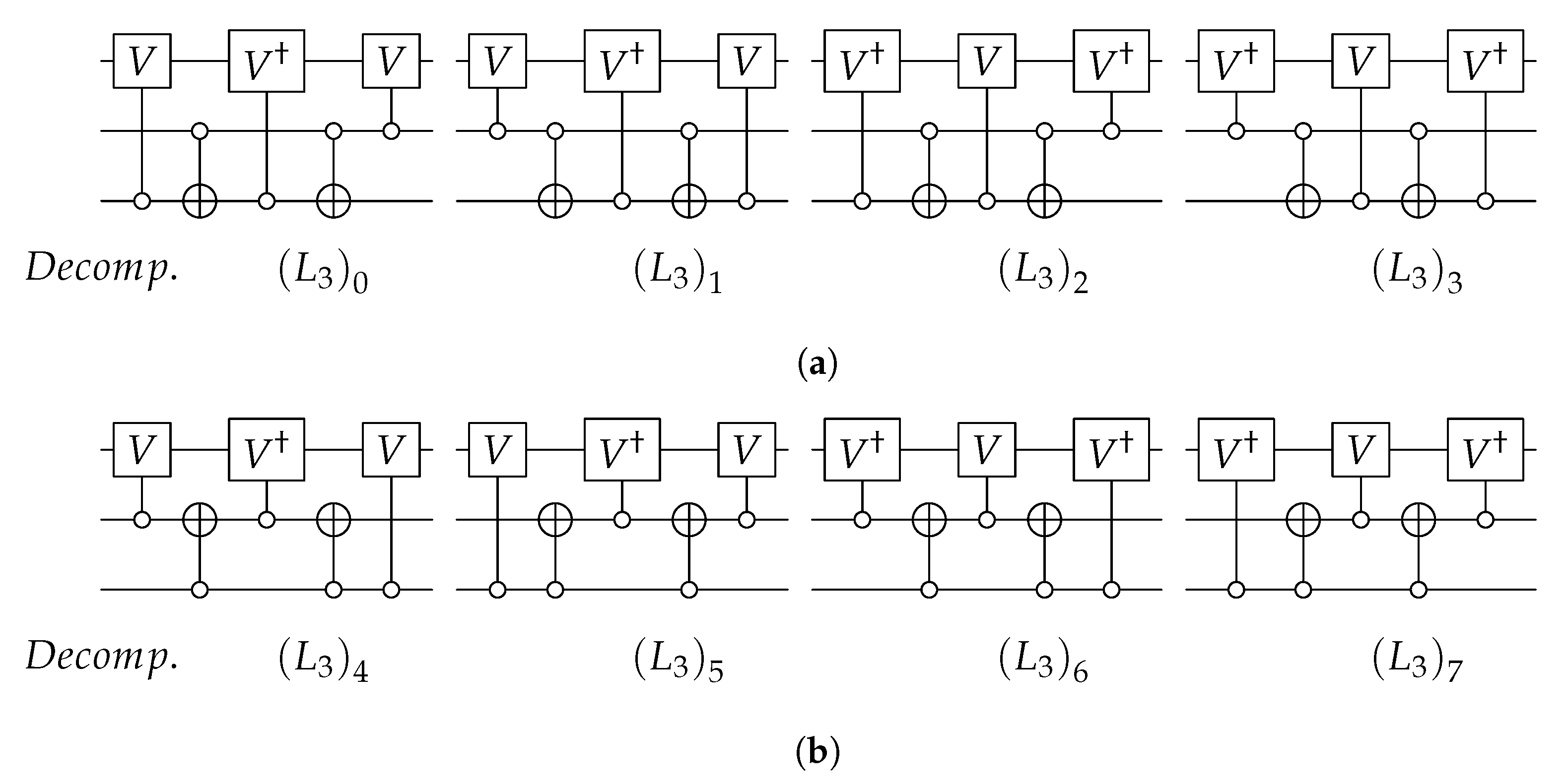
Figure 5.
basic pair where (a) represents the basic pair before optimization with a quantum cost of 10; (b) represents the basic pair after swapping the two marked gates and the solid box shows the gates that will be merged; (c) represents the basic pair after applying the merging rules, where two two-qubit gates are formed and the quantum cost is reduced to 8; (d) represents the basic pair after moving the marked gate to the right-hand side and marking the other resulting two-qubit gate; (e) represents the basic pair after moving the marked gate to the left-hand side and applying the optimization rules, where the dashed box indicates forming a two-qubit gate [15]; hence, the final quantum cost is 7.
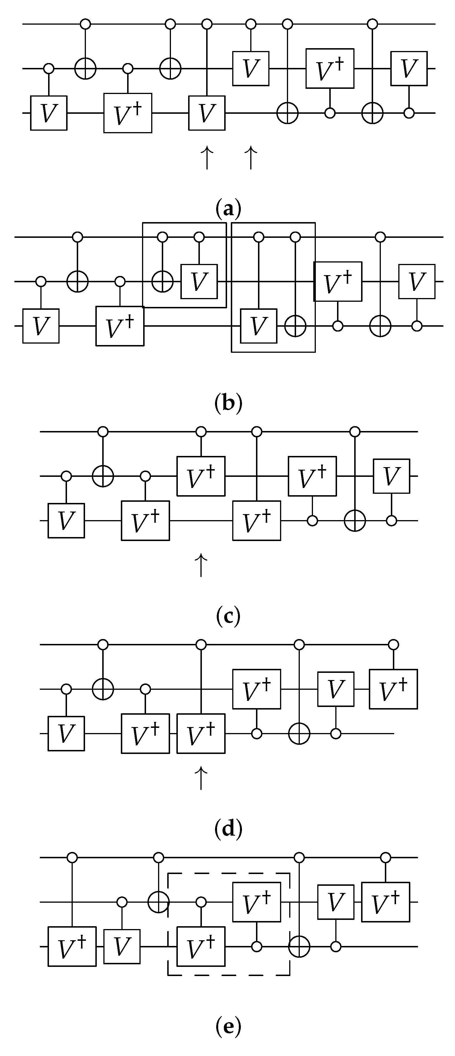
Figure 6.
Possible basic pairs for where the quantum cost is reduced. Q.C stands for quantum cost; (a) shows the lowest quantum cost of possible basic pairs with quantum cost of 4; (b,c) show possible basic pairs with quantum cost of 5.
Figure 6.
Possible basic pairs for where the quantum cost is reduced. Q.C stands for quantum cost; (a) shows the lowest quantum cost of possible basic pairs with quantum cost of 4; (b,c) show possible basic pairs with quantum cost of 5.

Figure 7.
Point of connection of basic pairs and in the circuit.
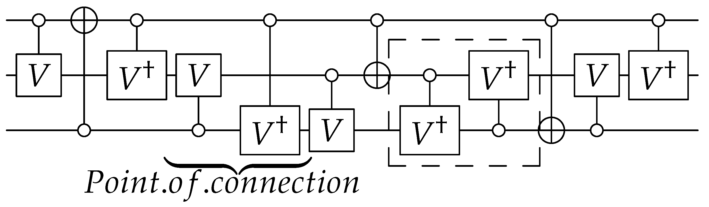
Figure 8.
The circuit where (a) represents the quantum circuit with a quantum cost of 17; (b) represents the reconstructed circuit using basic pairs of gates and a with a quantum cost of 12; (c) represents the quantum circuit after applying the optimization rules and forming a two-qubit gate. The final quantum cost after optimization is 11.
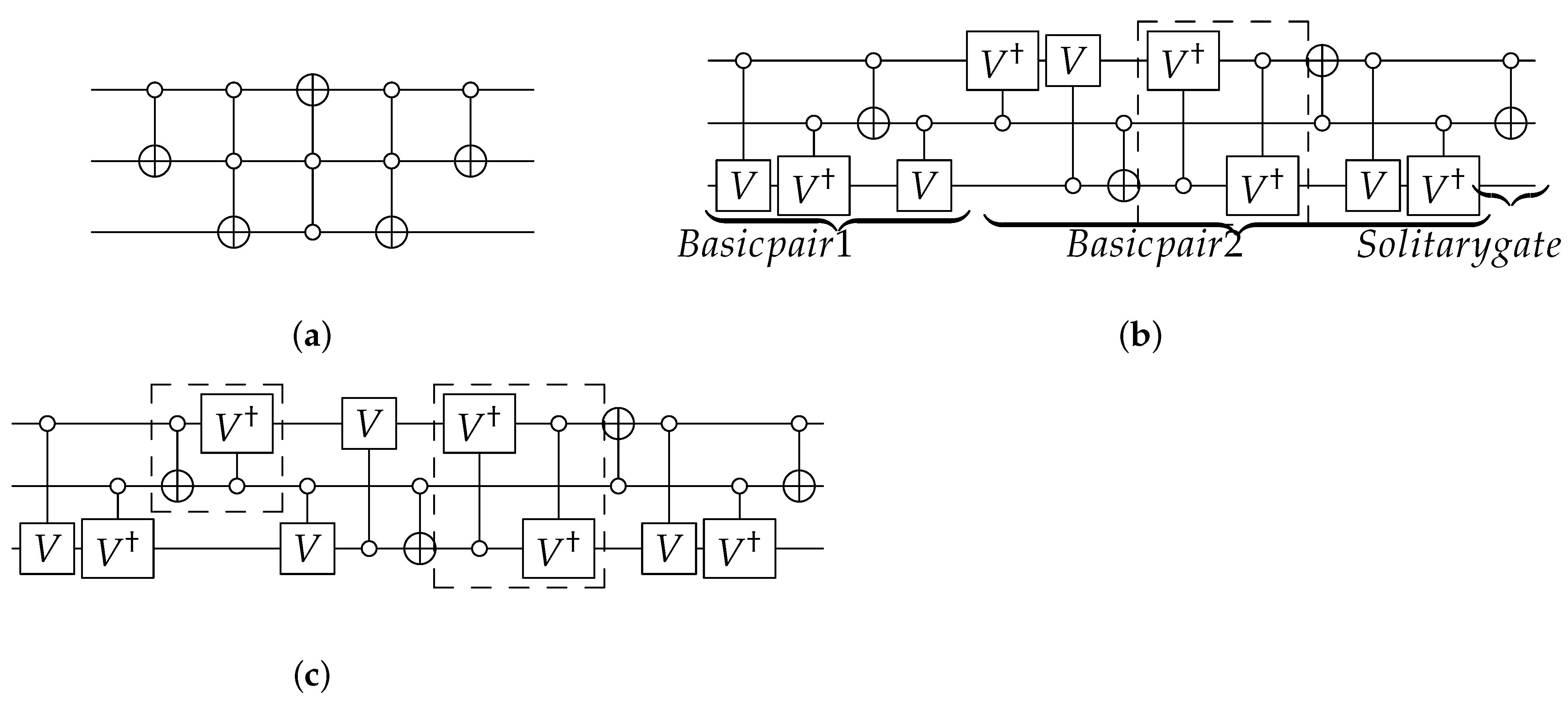
Figure 9.
The circuit where (a) represents the quantum circuit with a quantum cost of 11; (b) represents the quantum circuit, which is reconstructed by using FunctionI (Algorithm 1) with a quantum cost of 10; (c) represents the quantum circuit, which is reconstructed by using FunctionII (Algorithm 3) with a quantum cost of 8; (d) represents the quantum circuit, which is reconstructed using FunctionII (Algorithm 3) after applying the optimization rules on the points of connection and the final quantum cost is 7.
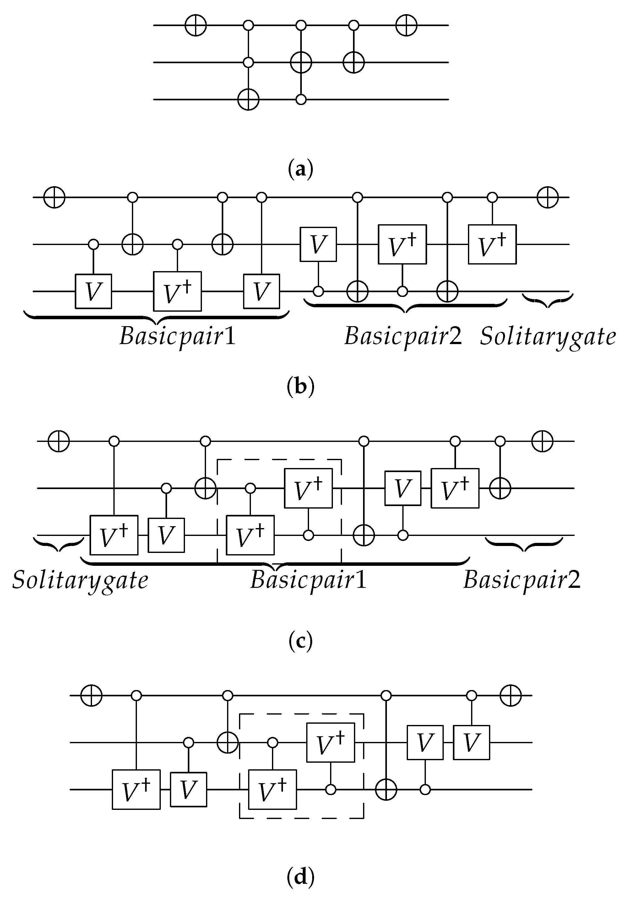
Figure 10.
Preparing the gate for IBM Quantum Experience implementation, where a negative control is equivalent to adding NOT gates before and after a positive control.
Figure 10.
Preparing the gate for IBM Quantum Experience implementation, where a negative control is equivalent to adding NOT gates before and after a positive control.
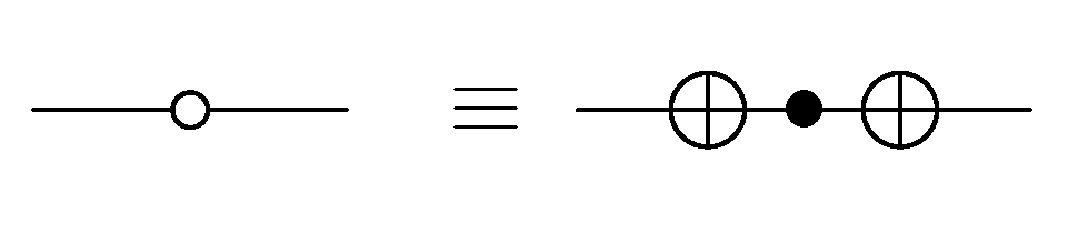
Figure 11.
The circuit implementation on the system, where the quantum cost of this circuit is 7. The solid box indicates merging the two gates to form gate; the dashed box indicates forming a two-qubit gate with a quantum cost of 1 [15].
Figure 11.
The circuit implementation on the system, where the quantum cost of this circuit is 7. The solid box indicates merging the two gates to form gate; the dashed box indicates forming a two-qubit gate with a quantum cost of 1 [15].
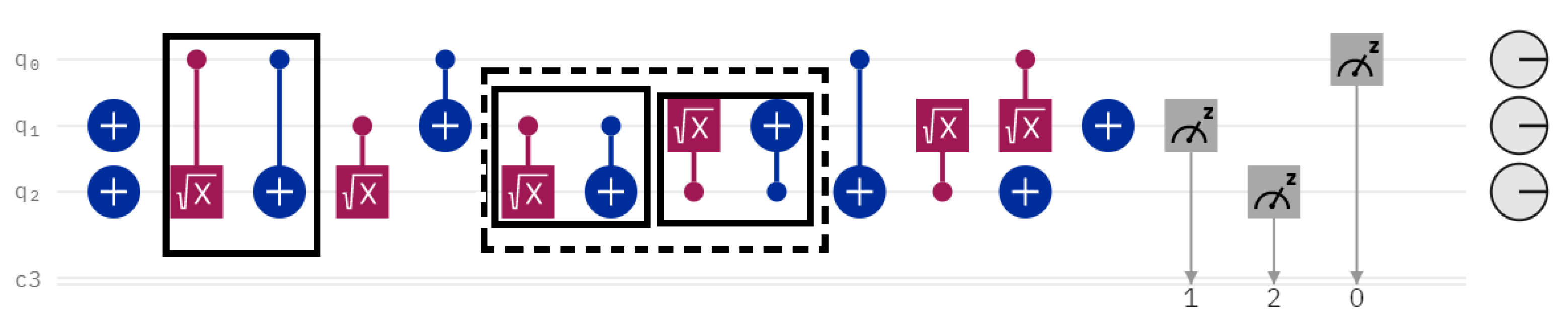
Figure 12.
The equivalent circuit using the NCT library, where (a) represents the quantum circuit with a quantum cost of 11 and (b) represents the circuit implementation on the system with a quantum cost of 11.
Figure 12.
The equivalent circuit using the NCT library, where (a) represents the quantum circuit with a quantum cost of 11 and (b) represents the circuit implementation on the system with a quantum cost of 11.

Figure 13.
The circuit, where (a) represents the quantum circuit with a quantum cost of 8, (b) represents the quantum circuit after optimization with a quantum cost of 6, and (c) represents the circuit implementation on the system with a quantum cost of 6. The dashed box indicates forming a two qubit gate and the solid box indicates forming gate.

Figure 14.
The equivalent circuit using the NCT library, where (a) represents the quantum circuit with a quantum cost of 15 and (b) represents the circuit implementation on the system with a quantum cost of 15.
Figure 14.
The equivalent circuit using the NCT library, where (a) represents the quantum circuit with a quantum cost of 15 and (b) represents the circuit implementation on the system with a quantum cost of 15.


Table 1.
The Truth table of NOT, CNOT, OCNOT , , , , Toffoli and OToffoli gates for three-qubit system.
Table 1.
The Truth table of NOT, CNOT, OCNOT , , , , Toffoli and OToffoli gates for three-qubit system.
| NOT Gate (N3) | |||
|---|---|---|---|
| Input | Output | ||
| CNOT | OCNOT | ||
| Input | Output | Input | Output |
| Input | Output | Input | Output |
| Input | Output | Input | Output |
| Toffoli | OToffoli | ||
| Input | Output | Input | Output |
Table 2.
The moving rules of quantum gates.
| Gate | Swappable Gates |
|---|---|
| , , , , , | |
| , , , |
Table 3.
The merging rules of quantum gates.
| Gates before Optimization | Gates after Optimization |
|---|---|
| , | I |
| I | |
| , | |
| , | |
Table 4.
Negative NCT gates with their corresponding gate symbol.
| Gate | Gate Sym. | Gate | Gate Sym. | Gate | Gate Sym. | Gate | Gate Sym. |
|---|---|---|---|---|---|---|---|
Table 5.
Negative NCT gates with their equivalent gate decomposition (Decomp.).
| Gate | Gate Decomposition | ||||
|---|---|---|---|---|---|
| Gate | Gate Decomp. | Gate | Gate Decomp. | Gate | Gate Decomp. |
Table 6.
Negative NCT gate decomposition with their corresponding and sets.
| Gate Decomposition | lg Set | rg Set |
|---|---|---|
| , | ||
| , | ||
| , | ||
| , | ||
| , | ||
| , | ||
| , | ||
| , | ||
| , | ||
| , | ||
| , | ||
| , | ||
Table 7.
Negative NCT library’s basic pairs, where BO refers to the quantum cost before optimization and AO refers to the quantum cost after optimization.
Table 7.
Negative NCT library’s basic pairs, where BO refers to the quantum cost before optimization and AO refers to the quantum cost after optimization.
| Negative NCT Library’s Basic Pairs That Include OCNOT or OToffoli Gates | ||||
|---|---|---|---|---|
| Pair of Gates | Gate Decomposition/Basic Pair | AO | BO | Basic Pair Circuit |
| 7 | 10 | |||
| 7 | 10 | |||
| 4 | 6 | |||
| 5 | 6 | |||
| 4 | 6 | |||
| 5 | 6 | |||
| 5 | 6 | |||
| 5 | 6 | |||
| 7 | 10 | |||
| 7 | 10 | |||
| 5 | 6 | |||
| 4 | 6 | |||
| 5 | 6 | |||
| 5 | 6 | |||
| 5 | 6 | |||
| 4 | 6 | |||
| 7 | 10 | |||
| 7 | 10 | |||
| 5 | 6 | |||
| 5 | 6 | |||
| 5 | 6 | |||
| 4 | 6 | |||
| 4 | 6 | |||
| 5 | 6 | |||
| 4 | 6 | |||
| 5 | 6 | |||
| 5 | 6 | |||
| 1 | 2 | |||
| 5 | 6 | |||
| 4 | 6 | |||
| 5 | 6 | |||
| 1 | 2 | |||
| 4 | 6 | |||
| 5 | 6 | |||
| 5 | 6 | |||
| 1 | 2 | |||
| 5 | 6 | |||
| 5 | 6 | |||
| 4 | 6 | |||
| 1 | 2 | |||
| 5 | 6 | |||
| 5 | 6 | |||
| 4 | 6 | |||
| 1 | 2 | |||
| 5 | 6 | |||
| 4 | 6 | |||
| 5 | 6 | |||
| 1 | 2 | |||
Table 8.
Comparing the quantum cost of the proposed Negative NCT library using the proposed optimization algorithms (Algorithms 2 and 4) with related work in cost015, where denotes the Negative NCT library’s specification before optimization. and denote the number of specification with minimum quantum cost produced by the proposed circuit optimization algorithm (Algorithm 2) and the proposed modified circuit optimization algorithm (Algorithm 4), respectively. The denotes the number of specifications with minimum quantum cost shown in [18], denotes the number of specifications with minimum quantum cost shown in [18], denotes the number of specifications with minimum quantum cost shown in [19], and denotes the number of specifications with minimum quantum cost shown in [15].
| Minimum Cost | NT [18] | NR3 [18] | NM3 [19] | NCT [15] | A0 | A1 Algorithm 2 | A2 Algorithm 4 |
|---|---|---|---|---|---|---|---|
| 0 | 8 | 8 | 8 | 8 | 8 | 8 | 8 |
| 1 | 0 | 0 | 0 | 48 | 48 | 109 | 111 |
| 2 | 0 | 0 | 0 | 324 | 189 | 488 | 459 |
| 3 | 0 | 0 | 0 | 607 | 402 | 467 | 459 |
| 4 | 0 | 192 | 192 | 601 | 465 | 604 | 705 |
| 5 | 94 | 0 | 0 | 1148 | 240 | 1319 | 1492 |
| 6 | 0 | 0 | 0 | 2462 | 366 | 2605 | 2594 |
| 7 | 0 | 851 | 2136 | 3576 | 1386 | 3204 | 3338 |
| 8 | 16 | 2591 | 1300 | 2710 | 3087 | 3844 | 4358 |
| 9 | 340 | 0 | 0 | 2855 | 2921 | 4159 | 4115 |
| 10 | 288 | 636 | 0 | 5601 | 537 | 4733 | 4408 |
| 11 | 32 | 6050 | 11,916 | 6567 | 1255 | 4342 | 4175 |
| 12 | 179 | 9354 | 4064 | 3183 | 4563 | 4184 | 4184 |
| 13 | 790 | 396 | 0 | 2043 | 7305 | 3693 | 3741 |
| 14 | 1487 | 2829 | 3294 | 3771 | 3141 | 2801 | 2711 |
| 15 | 324 | 7175 | 7242 | 3496 | 447 | 1488 | 1373 |
| 16 | 574 | 6331 | 6137 | 1284 | 2178 | 1020 | 983 |
| 17 | 2052 | 344 | 0 | 36 | 4819 | 680 | 648 |
| 18 | 3616 | 1200 | 1117 | 0 | 3809 | 280 | 240 |
| 19 | 1462 | 1278 | 1484 | 0 | 574 | 128 | 83 |
| 20 | 1041 | 1053 | 1387 | 0 | 501 | 79 | 66 |
| 21 | 3405 | 9 | 0 | 0 | 1185 | 57 | 48 |
| 22 | 5357 | 14 | 0 | 0 | 614 | 25 | 18 |
| 23 | 2894 | 2 | 0 | 0 | 37 | 3 | 3 |
| 24 | 1435 | 7 | 43 | 0 | 0 | 0 | 0 |
| 25 | 3191 | 0 | 0 | 0 | 149 | 0 | 0 |
| 26 | 4369 | 0 | 0 | 0 | 86 | 0 | 0 |
| 27 | 2436 | 0 | 0 | 0 | 4 | 0 | 0 |
| 28 | 806 | 0 | 0 | 0 | 0 | 0 | 0 |
| 29 | 1444 | 0 | 0 | 0 | 0 | 0 | 0 |
| 30 | 1482 | 0 | 0 | 0 | 4 | 0 | 0 |
| 31 | 761 | 0 | 0 | 0 | 0 | 0 | 0 |
| 32 | 125 | 0 | 0 | 0 | 0 | 0 | 0 |
| 33 | 126 | 0 | 0 | 0 | 0 | 0 | 0 |
| 34 | 109 | 0 | 0 | 0 | 0 | 0 | 0 |
| 35 | 60 | 0 | 0 | 0 | 0 | 0 | 0 |
| 36 | 6 | 0 | 0 | 0 | 0 | 0 | 0 |
| Avg | 22.321 | 13.388 | 13.290 | 10.348 | 13.364 | 10.202 | 10.078 |
Table 9.
Comparing the quantum cost of the proposed Negative NCT library using the proposed optimization algorithms (Algorithms 2 and 4) with related work in cost115, where , denotes the number of specification with minimum quantum cost produced by the proposed circuit optimization algorithm (Algorithm 2) and the proposed modified circuit optimization algorithm (Algorithm 4), respectively. The denotes the number of specifications of the NCT library with minimum quantum cost shown in [15].
| Minimum Cost | NCT [15] | B1 Algorithm 2 | B2 Algorithm 4 |
|---|---|---|---|
| 0 | 0 | 0 | 0 |
| 1 | 9 | 18 | 18 |
| 2 | 72 | 133 | 130 |
| 3 | 299 | 428 | 400 |
| 4 | 551 | 545 | 564 |
| 5 | 519 | 720 | 803 |
| 6 | 728 | 1334 | 1430 |
| 7 | 1715 | 2256 | 2371 |
| 8 | 2976 | 3315 | 3385 |
| 9 | 3060 | 3867 | 4064 |
| 10 | 2366 | 4099 | 4322 |
| 11 | 2923 | 4256 | 4110 |
| 12 | 4417 | 4336 | 4150 |
| 13 | 4717 | 4018 | 3918 |
| 14 | 3513 | 3625 | 3656 |
| 15 | 2637 | 2803 | 2777 |
| 16 | 2385 | 1711 | 1607 |
| 17 | 2260 | 1142 | 1046 |
| 18 | 2021 | 752 | 738 |
| 19 | 1543 | 464 | 427 |
| 20 | 994 | 225 | 191 |
| 21 | 474 | 127 | 91 |
| 22 | 130 | 73 | 67 |
| 23 | 10 | 47 | 32 |
| 24 | 0 | 20 | 17 |
| 25 | 0 | 4 | 4 |
| 26 | 0 | 1 | 1 |
| Avg | 12.591 | 11.333 | 11.209 |
Publisher’s Note: MDPI stays neutral with regard to jurisdictional claims in published maps and institutional affiliations. |
© 2021 by the authors. Licensee MDPI, Basel, Switzerland. This article is an open access article distributed under the terms and conditions of the Creative Commons Attribution (CC BY) license (https://creativecommons.org/licenses/by/4.0/).
Share and Cite
MDPI and ACS Style
Gado, M.; Younes, A. Optimization of Reversible Circuits Using Toffoli Decompositions with Negative Controls. Symmetry 2021, 13, 1025. https://doi.org/10.3390/sym13061025
AMA Style
Gado M, Younes A. Optimization of Reversible Circuits Using Toffoli Decompositions with Negative Controls. Symmetry. 2021; 13(6):1025. https://doi.org/10.3390/sym13061025
Chicago/Turabian StyleGado, Mariam, and Ahmed Younes. 2021. "Optimization of Reversible Circuits Using Toffoli Decompositions with Negative Controls" Symmetry 13, no. 6: 1025. https://doi.org/10.3390/sym13061025
Note that from the first issue of 2016, this journal uses article numbers instead of page numbers. See further details here.