Abstract
Thin-film organic solar cell (OSC) performances have been investigated in detail by improved analytical computation in this work. The generation of excitons inside OSC has been estimated by using the optical transfer matrix method (OTMM) to include the optical phenomena of the incident light. The dissociation of these excitons into free charge carriers has been investigated to find the most appropriate one. OSC performances have been evaluated by an improved analytical solution of electrical transport equations including (i) exciton generation obtained from OTMM, (ii) dissociation probability incorporating Gaussian distribution to account for the natural fact of the difference in photon-energy producing excitons, (iii) recombination of charge carriers, all together. OSC properties such as JSC, VOC, FF, PCE, Pmax, absorbance, and quantum efficiency have been investigated with the variation of different parameters; this might be useful to improve OSC. Again, the presented detailed derivations of analytical expressions would be helpful for clear understanding.
1. Introduction
An organic solar cell (OSC) looks like a good candidate for harvesting solar energy because it has some advantageous features compared to its counterpart conventional Si solar cells [1,2,3]. OSCs are basically made of layers of different materials; one layer is photoactive which consists of two organic materials such that one organic material (usually conjugated polymer) has the property to donate electrons and another organic material (usually fullerene) has the property to accept electrons, i.e., donor and acceptor. Due to light absorption in the photoactive layer, excitons (firmly bounded electron-hole-pairs) are generated. Then these excitons are dissociated into free charge carriers (electrons and holes). Dissociation occurs when excitons interact with donor-acceptor interfaces, defects, etc.; donor-acceptor interface has an internal electric field like a pn junction diode; therefore, this interface is the most effective site for dissociation. A bi-layered OSC has only one donor-acceptor interface; only the excitons, generated very near to this single interface, can reach the interface and be dissociated. However, for bulk hetero-junction (BHJ) OSC, the active layer is made of a mixer of donor and acceptor materials, lots of donor-acceptor interfaces, hence almost all generated excitons can get nearby interface and can be dissociated. As a result, BHJ OSC is more efficient than bi-layered OSC; therefore, many people [4,5,6] are working with BHJ OSC for its improvement. Some researchers [7] reported BHJ OSC with the internal quantum efficiency of 100%; but the useful external efficiency is only 10%.
For the further improvement of BHJ OSC, works regarding the structure and/or layer materials are required. The theoretical analysis (physics-based/simulation) can help in this regard. Some theoretical works have been done by numerical methods [8,9,10,11] and some other works have been done with analytical calculations [12,13,14].
Although few numerical methods are robust regarding initial guesses, for most of the numerical methods it is observed that they are complicated and highly dependent on an initial guess, whereas, analytical calculation provides more correct results directly without the need for an initial guess. In this work, BHJ OSC will be investigated using analytical calculations. The accuracy of the analytical result depends on the way of treating the generation of excitons, dissociation of excitons into charge carriers, and recombination of charge carriers.
Regarding the use of generation rate in analytical calculations, some researchers [12] utilized empirical fitting quantities; some other group [14] used constant generation rate for making analytical calculations easier. However, for a thin layered device like OSC, constant generation rate approximation is not suitable, because due to thin layer, the incident light will not be reduced to zero while passing a layer, and hence it will be reflected and refracted at the interface with next layer, then there will be interference between incident-light and reflected-light, hence, the resultant light intensity will be different at different positions. As a result, the excitons will be different at different positions, i.e., excitons will be position dependent. Many researchers used exciton generation rate exponentially decreasing with position (Beer–Lambert law), but this neglects the impacts of optical phenomena (refraction, reflection, and interference). However, for the thin layered device, the effects of optical phenomena cannot be ignored, hence exponentially decreasing generation rate model would not be suitable also. Again, depending on the bandgap size of active layer material, photons with some wavelengths will be absorbed effectively, some other wavelengths will not be so effective, that is, the exciton generation will also depend on wavelength. The Optical Transfer Matrix Method (OTMM) considers the effects of optical phenomena and wavelength-dependent properties of layer materials, hence OTMM provides the generation rate as the function of both position and wavelength [3,11,15,16]. Therefore, the OTMM-based generation rate is most suitable for thin layered OSC and hence it has been used in this work for a more accurate result.
Regarding recombination, we see that many analytical works [14,17,18,19] neglected recombination; but recombination is a vital factor as it affects current and other performances [20]. Some analytical works considered recombination, but they used generation rate either constant [21] or exponentially decreasing [22]; however, as stated earlier, the constant or exponential model is not as accurate as the OTMM-based generation rate for the thin layered device. Some other works [18,19] used OTMM based generation rate but neglected recombination.
Another factor is the dissociation rate function used for calculating dissociation probability for computing charge carriers from the excitons. Based on Onsager’s theory [23], Braun introduced the dissociation rate function [24]. Previous researchers [8,11] used the Braun model, and recently, people [21,25] are using the Wojcik and Tachiya model which is an improved version of the Braun model. Both models used constant (same) separation distance between electron and hole for all excitons. However, naturally, for any device, the electron-hole-separation distances will be different for different excitons because of the difference in photon-energy producing excitons. To address this fact, a standard distribution function may be applied along with Braun or Wojcik model.
To the best of my knowledge, in literature, no analytical work on OSC considered (i) OTMM-based exciton, (ii) dissociation probability including standard distribution function, (iii) recombination of charge carriers, all together. While including all these three factors together, the analytical solution becomes complicated, however, it is assumed necessary to get a better result. Again, most of the reported works usually calculate J-V, P-V, efficiency for a fixed condition; there are few works on the investigation with the variety of different factors, especially, no investigation work used above factors altogether. Moreover, almost all reported analytical works presented the final form of analytical expressions, no details about the derivation, in that case, it does not become clear about the limitations or assumptions used in the derivation.
To fill the aforementioned deficits in literature, this work has been done with the following targets. Target 1: Improved analytical calculations of OSC performances including the following three factors all together: (i) exciton generation rate obtained from OTMM to include optical phenomena, (ii) dissociation probability obtained by incorporating Gaussian distribution to consider the natural fact of the difference in electron-hole-separation distances, (iii) recombination of charge carriers. Target 2: Analysis of different OSC properties in detail with the variation of terminal voltage, irradiance, wavelength, active layer thickness using the above-mentioned improved analytical calculation. Target 3: The detailed derivations of analytical expressions with a view to making the work clear regarding limitations and assumptions and easy understanding for the OSC researchers, especially, for the new ones.
2. Excitons
When light falls on thin-layered OSC, excitons are generated by photons inside the photo-active layer (organic material). The distribution of light (hence the distribution of excitons) inside the active layer may be obtained by using the Optical Transfer Matrix Method (OTMM). Many works used OTMM-based equations. However, detailed derivation of OTMM-based equations is being presented here for better understanding.
Let us consider m layer (thin) device sandwiched between air and substrate (thick) as shown in Figure 1. The air is designated as layer and the substrate as layer.
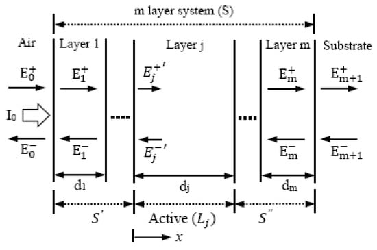
Figure 1.
Thin-layered device consisting of m layers of different materials. The device is situated between air and substrate.
According to OTMM, while light crosses the interface of layer 0 and layer 1, the refraction and reflection behavior of light may be expressed by an interface matrix , for perpendicular light falling, as follows [11].
where, and are complex refractive indices of layer 0 and layer 1.
Again, according to OTMM, while light passes through layer 1, the absorption behavior of light may be expressed by a layered matrix , for perpendicular light falling, as follows [11].
where, ; thickness of layer 1; change of phase angle as the light passes through the layer 1.
Similarly, calculating all interface matrices and layer matrices, for the whole structure, a scattering matrix (transfer matrix) may be formed as follows.
At any position inside the device, the optical electric field () has two components: (forward component along positive ) and (backward component along negative ) as shown in Figure 1.
The components of inside layer may be related to those inside layer via the matrix as follows.
As the substrate is thick, no reflected light inside substrate, i.e., . Using in the above equation, we may get, and . Now for whole system, we may get reflection coefficient, and transmission coefficients, .
To determine the distribution of light (hence distribution of excitons) inside the active layer ( layer), we need to treat the active layer matrix separately. Therefore, the matrix may be divided into three segments such that .
Like the whole system (), reflection and transmission coefficients for subsystems ( and ) may be defined as ; ; ; .
Assuming the left edge of the layer is = 0, the optical electric field at a position inside the layer can be written as
If we assume and as the forward and backward field components at the beginning of layer (Figure 1), then we get Equation (8) (see Appendix A).
If we define an internal forward transfer coefficient () as then we get Equation (9) (see Appendix B).
The value of may be found by the Equation (10) (see Appendix C).
As is a complex term, it can be expressed in polar form as where are the magnitude and angle of . By putting and in Equation (9), we get
Putting in Equation (11) and algebraic manipulation gives the Equation (12) (see Appendix D).
where, .
Note that, is the absorption coefficient (unit: m−1).
Assigning, we may write Equation (12) as
Irradiance () may be expressed as, = , where light speed, = electric permittivity, = vacuum permittivity, = relative permittivity or dielectric constant, = electric field (see Appendix E).
Accordingly, the irradiance at position x in layer is,
Using the relation between refractive index and electric permittivity, may be expressed by Equation (15) (see Appendix F).
If the irradiance (unit: Wm−2 or Js−1m−2) is multiplied with absorption coefficient (unit: m−1), it will give the power dissipated per unit volume as (unit: Js−1m−3). We know, photon energy (unit: J); where Planck’s constant. If we divide by photon energy, we will obtain absorbed photon rate per unit volume () (unit: s−1m−3) as
Like many other researchers [11], it may be assumed that each photon produces one exciton in P3HT: PCBM based OSC. Therefore, the exciton generation rate per unit volume, (unit: s−1m−3) would be equal to .
3. Charge Carriers
Excitons are dissociated into free charge carriers (electrons and holes). To calculate these free charge carries, we need to use dissociation probability. Geminate recombination theory of Onsager [23,26,27] may be employed to calculate dissociation probability.
Braun [24] tried to correct Onsager’s theory using a model as follows: any exciton may decay to ground state (recombine) or dissociate into free charge carriers; if the decay rate is and the dissociation rate is then dissociation probability (P) is,
The decay rate is inversely proportional to separation distance () between electron and hole of an exciton, that is, , where is the reactivity parameter (unit: ms−1). The electric field () plays the main role in dissociation, that is, . Using the work of Onsager [28], Braun introduced a formula of including the effect of as follows.
Here, recombination rate constant; = electronic charge value; = electron (hole) mobility (unit: m2V−1s−1); binding energy of electron-hole-pair of an exciton; = Boltzmann’s constant; temperature in Kelvin; first-order Bessel function of the first kind; field parameter; = electric field (unit: Vm−1).
Many researchers [8,11,29,30] used Braun’s formula of to calculate dissociation probability. However, for better results, Wojcik et al. [21,26] proposed a modified formula of as given below.
where, ; electron diffusion coefficient (unit: m2s−1); = hole diffusion coefficient; = Onsager radius.
Braun or Wojcik formula used constant value for separation distance [21,24,25,26]. However, separation distances are different, therefore, the probability may be calculated by Equation (23) (see Appendix G).
where, is spherically averaged Gaussian distribution (SAGD) function given by
where, = separation distance corresponding to peak of SAGD function.
Note that, .
After getting , charge carrier generation rate, (unit: s−1m−3) can be found as
where .
4. Device Structure
The organic solar cell (OSC) analyzed in this work is a layered device as shown in Figure 2a. The energy levels of layer materials, shown in Figure 2b, are taken from previous works [3,7,11,31,32,33,34,35]. Usually, the energy band diagram shows the electron energy, therefore, all energy levels are shown with a negative sign (negative charge energy).
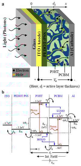
Figure 2.
P3HT: PCBM-based Organic Solar Cell: (a) structure, (b) energy band diagram.
Naturally, low energy states are easily filled with electrons and higher energy states remain vacant. The conduction band is the lowest energy level(s) among the vacant states and the valence band is the highest energy level(s) among the filled states. Semiconductor behaviors are explained with a conduction band and valence band separated by an energy gap. Similarly, organic materials (P3HT, PCBM) behavior may be explained with LUMO (lowest unoccupied molecular orbital) and HOMO (highest occupied molecular orbital) separated by an energy gap. The mixer of P3HT and PCBM is the active layer where photons are absorbed. Active layer may be thought of as a single meta-material considering PCBM_LUMO like conduction band and P3HT_HOMO like valence band [9,10,12,14]; bandgap = (PCBM_LUMO–P3HT_HOMO) = 1 eV.
After absorbing photons, excitons are generated; for some excitons, electrons, and holes are recombined; for other excitons, electrons and holes are separated and become free. Then free electrons move from P3HT_LUMO to PCBM_LUMO and free holes move from PCBM_HOMO to P3HT_HOMO shown in Figure 2(b). P3HT is (electron) donor and PCBM is (electron) acceptor. Even after movement, electrons at PCBM_LUMO and holes at P3HT_HOMO form “geminate pairs”. Afterward, these pairs are broken by the electric field and thus electrons and holes become finally free to move.
Then, finally free electrons flow from PCBM_LUMO to and free holes flow from P3HT_HOMO to ITO via PEDOT: PSS, as in Figure 2b.
Electron-flow from P3HT to PCBM produces a current in the direction of PCBM to P3HT; hole-flow from PCBM to P3HT produces a current in the direction of PCBM to P3HT, that is, both flows produce current in the direction of PCBM to P3HT inside the device. We know, for a pn junction solar cell, the current is in the direction of n-Si to p-Si; therefore, it may be deduced that P3HT is like p-Si and PCBM is like n-Si.
As there is a current in the direction of PCBM to P3HT without the application of any external voltage, we may perceive an internal electric field inside the active layer in the direction of PCBM to P3HT (same direction of current) that causes the flow of photo-generated electrons and holes and produces the current. Both current and internal fields (PCBM to P3HT direction) are negative because conventionally the direction of P3HT to PCBM is considered positive. Corresponding to this internal field, we may perceive an internal built-in potential as shown in Figure 2b. This may be determined by the difference of energy levels of and PEDOT: PSS [12,14,31] which are adjacent to both sides of the active layer.
When a battery is connected to this OSC for charging, the current will come out at ITO and will charge the battery, therefore, the battery terminal which is connected to ITO will have positive polarity. Now, the battery voltage will work as the externally applied voltage (say ) with battery-positive at ITO (i.e., P3HT side or p-side) and battery-negative at (i.e., PCBM side or n-side), that is, will work for forward biasing the device. This will provide an electric field in the direction of P3HT to PCBM; this field is positive. Therefore, the resultant electric field inside the active layer would be , where = active layer thickness.
While the electrons and holes move, some of them may be lost due to recombination within the active layer. Recombination has been considered in this work.
Here, a glass-layer has been used for the mechanical support and protection for thin layers of materials. PEDOT: PSS has been used to guide and collect holes effectively by making small energy step favorable for holes to move.
5. OSC Performances
Due to recombination and other interactions inside the device, all the generated charge carriers would not be useful for producing current. The electron current density due to current-producing electron can be expressed as follows [36].
Note that, here is electron density per unit volume (unit: m-3), not the electron rate.
The continuity equation for electrons at a steady-state would be as follows [36].
where, G = charge carrier (electron) generation rate (unit: s−1m−3), = electron recombination rate = , where, is the monomolecular recombination coefficient (unit: s−1).
In this work, F has been assumed constant like other works [10,12,13,14] and monomolecular recombination has been used to obtain a complete analytical solution (see Appendix H).
Using Equation (26) and Equation (27) we may obtain as
For the electrons due to environment temperature (dark condition), ; the differential equation is
The solution of the differential Equation (29) is
For the electrons due to photons, ; the differential equation is
The complementary solution of the differential Equation (31) is
where ““ stands for photon and it represents a photo-excited part.
The particular solution of the differential Equation (31) can be expressed by Equation (33) (see Appendix I).
where,
Electron due to the light for a single wavelength, would be the summation of and .
Total electron () may be expressed as
Using the boundary values of electron concentration at and in Equation (35), we will obtain the values of [see Appendix J].
Effective density of states at PCBM LUMO
Electron injection barrier potential at , see Figure 2b
Electron injection barrier potential at , see Figure 2b
Thermal voltage
By putting from Equation (30) into Equation (26), we may obtain electron dark current as
By putting from Equation (34) into Equation (26), we may obtain electron current due to the light of single wavelength as
Total electron current may be expressed as
Similarly, for the case of holes (, the differential equation would be
Similar solutions for holes are as follows
Using the boundary values of hole concentration at and in Equation (49) we will obtain the values of
Effective density of states at P3HT HOMO
Hole injection barrier potential at , see Figure 2b
Now the hole current.
Total current due to electron and hole is
It is obvious that electron and hole currents are the functions of position (); therefore, total current will also be the function of position. However, the total current should be position independent. By taking the average, the position-independent total current () may be obtained as follows [37,38].
The J-V characteristic can be analytically calculated by using Equation (61). Similarly, the other external properties such as the open-circuit voltage (VOC), short circuit current (JSC), maximum power (Pmax), fill factor (FF), power conversion efficiency (PCE) can be analytically calculated.
Again, the internal properties such as absorbance, external quantum efficiency (EQE), internal quantum efficiency (IQE) of OSC can be analytically evaluated as follows.
Absorbance is the ratio of the number of absorbed photons to the number of incident photons. Absorbance can be analytically expressed by the Equation (62) (see Appendix K)
Quantum efficiency indicates the effectiveness of the device to convert optical energy to electrical energy. External quantum efficiency (EQE) is the ratio of the number of photocurrent-producing charge carriers to the number of incident photons. Average photocurrent () and hence EQE can be determined as follows (see Appendix L).
Internal quantum efficiency (IQE) is the ratio of the number of photocurrent-producing charge carriers to the number of absorbed photons.
As absorbance is less than unity, IQE would be always larger than EQE.
6. Results and Discussions
An organic solar cell (OSC) having the structure “Glass/ITO/PEDOT: PSS/P3HT: PCBM/” has been investigated in this work.
Figure 1 shows the device structure to describe the theory of Optical Transfer Matrix Method (OTMM), as per theory in literature, light is incident from air to layer-1 and proceeds, OTMM theory defines the material after the last layer (layer-m) as the substrate, which is thick, no reflected light inside the substrate. In the device structure concept, the “Glass” layer is usually called the substrate since the whole device is built on it. The “substrate” in OTMM theory is not the same as “substrate” in the device structure concept. In the above-mentioned device structure, light is incident on the glass and proceeds, if we apply the OTMM equation in the same direction of light, will be the last layer, the “air” after layer will be considered as the substrate, the (m + 1)th layer for calculation.
The refractive index (), extinction coefficient (), and the thickness of the layers are used to calculate interface matrices and layer matrices by Equations (1) and (2) defined by the Optical Transfer Matrix Method (OTMM). Then the elements of these matrices and the solar irradiance (Io) are used to calculate generated excitons by the derived analytical equation. Then charge carriers, current, power, etc. are calculated by the corresponding analytical equations using these excitons. Thus, the derived analytical equations include the device structure size, material property, and solar light intensity in the calculation of OSC performances.
Spectral values of and of the materials, used for the OSC device, have been collected from literature [31].
The solar light intensity of a place depends on whether the Sun is at the vertical position or at an inclined position relative to that place, the inclination is represented by an index, called air mass (AM). Like many other researchers [2,3,7,8,11,14,20,21], this work has used solar irradiance of AM 1.5 (global) taken from standard source (ASTM G-173-03) [39].
The Equation (18), derived from OTMM, provides the generation rate of excitons as the function of position (x) and wavelength . The equation requires Io with the unit of Wm−2; however, in the standard dataset [39], irradiance Io is recorded with the unit Wm−2nm−1 (i.e., Wm−2 per nanometer bandwidth of wavelength), therefore, for calculating photo-excited part of any quantity (exciton, charge carrier, current) integration with respect to for the range of effective wavelengths is needed; when integrated wrt , then (which has the unit nm) cancels nm−1 part of Wm−2nm−1 then Io carries the required unit Wm−2 and hence the calculated (integrated) quantity is obtained with the standard unit.
Regarding the wavelength range, for the analysis of similar devices, some groups [11] used the wavelength range of 350–800 nm; some others [27] used the range of 350–850 nm; in this work, the wavelength range of 350–850 nm has been used.
To see the effects of optical phenomena on the exciton generation, and hence to see the suitability of using OTMM, the spatial distribution of excitons has been investigated. For a position inside the active layer, total exciton for all wavelengths has been evaluated by integrating the exciton obtained using OTMM based Equation (18) over the wavelength range of 350–850 nm. Similarly, the total excitons for all positions have been evaluated and hence the spatial variation of excitons has been obtained. Figure 3 shows the spatial variation of exciton generation rate inside active layer of OSC shown in Figure 2a with the irradiance of 1000 W/m2 for active layer thickness (dj) of 70, 100, 150, 250, 500, 1000 nm. The result of OTMM shows wave-like (pulsating) variation of exciton generation rate with the position; due to interference of incident light and reflected light the light intensity becomes stronger or weaker at places and hence pulsating variation of excitons occurs. The figure also shows that as the active layer thickness increases, the variation pattern changes from pulsating nature towards decreasing nature. When active layer thickness is very large, the variation exhibits an exponentially decreasing nature which is the same as stated by Beer-Lambert law; the agreement with “law” validates the use of the OTMM. The peak value of exciton generation rate is found in the range of 8 × 1027 − 20 × 1027 s−1m−3 (≡8–20 s−1nm−3). The pattern of variation and level of values are consistent with the reported results [10,17,40]. The pulsating variation confirms the effects of optical phenomena, that is, OTMM provides the correct profile of excitons considering optical phenomena and hence suitable for thin layered OSC research.
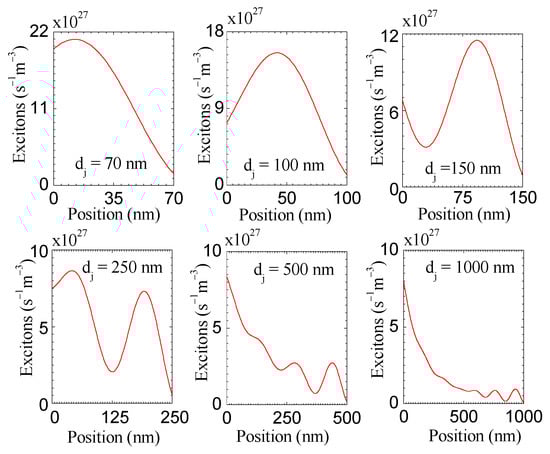
Figure 3.
Excitation generation rate per unit volume (s−1m−3) versus position inside active layer. For low active layer thickness, the exciton rate exhibits wave-like behavior with the position, whereas, for very large active layer thickness, the exciton rate exhibits exponentially-decreasing-like behavior with the position.
To find the appropriate dissociation probability, it has been calculated by Equation (19) using dissociation rate of Braun’s formula given in Equation (20) and of Wojcik’s formula given in Equation (22) and then calculated by Equation (23) incorporating Gaussian distribution function. Some researchers [8,11,29,30] used Braun’s formula and some others [21,25] used Wojcik’s formula, they used a constant value of separation distance () between electron and hole of an exciton, however, the separation distance value, used in the calculation, should be a representative value for all excitons, we may perceive as the average value. To find the appropriate value, the separation distance () has been taken as a variable (not constant) and dissociation probability has been calculated using Braun’s formula and Wojcik’s formula. Figure 4a shows the variation of dissociation probability with separation distance () for four-terminal voltages () of 0 V, 0.2 V, 0.4 V, and 0.6 V, calculated using Wojcik’s formula. For a certain (i.e., certain field), with the increase of separation distance (), dissociation probability is found to increase from zero to unity. This is logical because when the separation distance is larger, electron-hole-pair (EHP) of that exciton is loosely bounded, hence more feasible to dissociate, therefore, higher dissociation probability. Now the question is, which value of dissociation probability (i.e., which value of separation distance) should be used? The probability increases almost linearly from 0 to 1, hence the average (middle) value of probability (0.5) may be accepted as the representing value for probability; therefore, its separation distance may be assumed as the average separation distance and may be accepted as the representative value for . However, we see in Figure 4a that the probability value of 0.5 happens with a smaller for a smaller and vice versa. This is also logical because we know field . We know increases from zero, when becomes equal to , the field becomes zero, the solar cell stops to charge the external battery, that is, cannot be larger than , the field cannot be positive, the field is always negative (hence current is negative). When , field magnitude is the largest, when increases from zero, field magnitude decreases. For smaller , field magnitude is larger which becomes capable to dissociate EHP with lower separation distance (even they are strongly bounded) and hence the probability of 0.5 occurs at lower . Similarly, for larger , the probability of 0.5 occurs at higher . The separation distances, corresponding to the probability of 0.5, have been investigated for solar cell working range ; the average of these separation distances has been obtained as 1.51 nm, which may be used as the representative value for in calculation; this average value (1.51 nm) is consistent with the constant value used for separation distance in previous works [21,25].
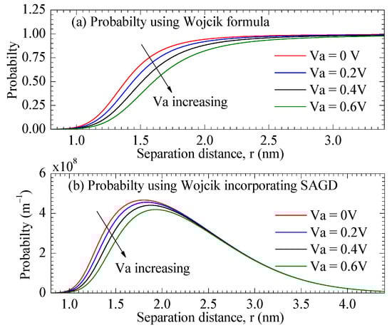
Figure 4.
Dissociation probability calculated using (a) Wojcik’s formula, (b) Wojcik’s formula incorporating spherically averaged Gaussian distribution (SAGD) function.
However, the concept of using a constant value of assumes that all excitons have the same separation distance, again, the concept of using the average value of assumes that the population of excitons would be the same at all separation distances; but both these assumptions are not compatible because naturally separation distances would be different and also population would be different.
To commensurate with the natural situation, spherically averaged Gaussian distribution (SAGD) may be incorporated in the calculation of dissociation probability as in Equation (23). For every separation distance (), the probability value (calculated by Braun’s formula or Wojcik’s formula) is multiplied with the SAGD function value at that separation distance to obtain SAGD incorporated probability. Figure 4b shows the SAGD incorporated probability versus for four-terminal voltages () of 0 V, 0.2 V, 0.4 V, and 0.6 V, calculated using Wojcik’s formula incorporated with the SAGD function. Note that Figure 4b shows the plotting of the integrand of Equation (23) and it has the unit of m−1.
The dissociation probability has been calculated by using Braun’s formula, Wojcik’s formula, and Wojcik’s formula incorporating SAGD function and compared; Figure 5 shows the comparative picture of the probability with the variation of for solar cell operation range ( 0–0.6 V). For Braun’s and Wojcik’s formulae, the separation distance of m has been used. To obtain the overall value of SAGD incorporated probability, Equation (23) needs to be integrated, that is, the curve in Figure 4b needs to be integrated. The integrand of Equation (23) is not integrable analytically, the integration has been computed numerically. Ideally, the integration range should be = 0 to ∞. From the analysis it was found that for m or less, the value of the integrand is negligible (order of ) compared to the highest value (order of ), similarly, for m or more, the value of the integrand is negligible, therefore, numerical integration has been carried out for the range m to m.
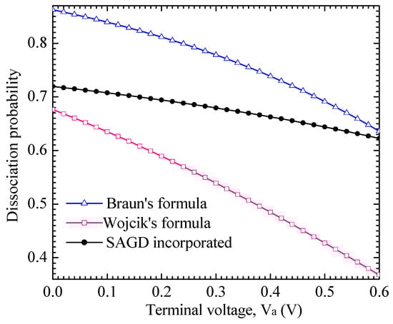
Figure 5.
Comparison among the probabilities obtained by Braun’s formula, Wojcik’s formula, and Wojcik’s formula incorporating SAGD function for solar cell operation range ( 0–0.6V). The probability decreases with .
For all three methods, the overall probability was found to decrease with the increase of . This is logical because, with the increase of , the field magnitude decreases, hence the dissociation probability decreases.
For solar cell operation range, i.e., for 0–0.6 V, Braun’s formula, Wojcik’s formula, and SAGD incorporated formula provide the dissociation probability values of 0.63–0.86, 0.36–0.67, and 0.62–0.72, respectively. For a similar device (P3HT:PCBM-based), some researchers [41] reported the dissociation probability of 0.4–0.74 for 0–0.6 V with constant separation distance. Some other works [42,43] reported the dissociation probability as the function of effective voltage. As the externally applied voltage and internal built-in voltage work in the opposite direction, the effective voltage may be defined as, ; in this work, is 0.8 V, therefore, for solar cell operation range, 0.2–0.8 V. For the same range of , Tan et al. [42] reported a probability of 0.6–0.78 and Hao et al. [43] reported a probability of 0.5–0.8. The dissociation probability values obtained in this work are consistent with the values reported in other works. Figure 5 shows that Braun’s formula provides a higher value of dissociation probability, Wojcik’s formula provides a lower value and SAGD incorporated calculation gives the value in between them. The SAGD incorporated probability is thought to be most appropriate because of considering naturally expected population variation of excitons, therefore, this probability has been used in this work.
The current-producing electron density per unit volume has been calculated by using Equation (35) which is the analytical solution of the differential Equation (28), then analytical results have been compared with those obtained by numerical solution of the same differential equation. Similarly, current-producing hole density has been calculated using analytical Equation (49) and compared with the numerical result. Figure 6a,b show the variation of current producing electron and hole density with the positions inside active layer for OSC having an active layer thickness of 100 nm operated at with an irradiance of 100 mW/cm2. Analytical results (solid lines) are exactly matched with numerical results (markers); this indicates that analytical solutions (expressions) are correct. The charge carrier density for the stated condition is found to vary in the order from 1020 m-3 to 1024 m-3 inside the active region as shown in Figure 6, the average value is in the order of 1023 m−3. For a similar device, some researchers [44] reported a charge density of 6×1015 cm-3 (≡ 6×10²¹ m-3); another group [45] reported a charge density in the range from 1021 m-3 to 1023 m-3; the charge density in this work is found consistent with previous reports. Note that, for numerical solution of differential equation, “bvp4c” solver, a built-in routine of MATLAB, has been used.
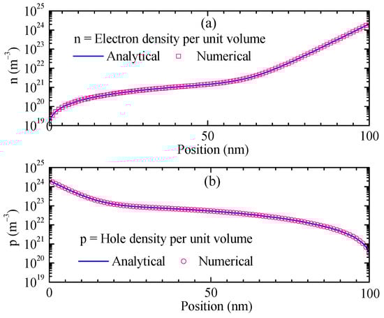
Figure 6.
Analytical and numerical results of current-producing electron density and hole density per unit volume for the OSC with an active layer thickness of 100 nm, irradiance 100 mW/cm2, terminal voltage 0.3V.
For a certain device [22], the total current density has been analytically calculated using Equation (61) at different values of for four levels of irradiance 100, 80, 60, and 40 mW/cm2, and the analytical results have been plotted along with experimental values. The analytical and experimental results [22] are in good agreement as shown in Figure 7a. Again, the dark component of current has been calculated by the summation of the dark current due to electron by using Equation (43) and dark current due to hole by using Equation (57). Similarly, the photo-exited component has been calculated by the summation of the photocurrent due to electron by using Equation (44) and photocurrent due to hole by using Equation (58). The extracted dark current and photocurrent for the irradiance of 100 mW/cm2 have been presented in Figure 7b. The separation of dark current and photo-current gives a better view than the plotting of total current only.
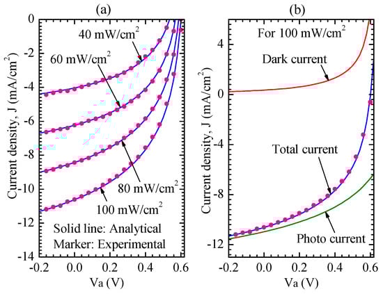
Figure 7.
(a) Analytically calculated current density (solid line) and experimental results of current density (circular marker) [22] for four levels of irradiance 100, 80, 60, and 40 mW/cm2; (b) Extraction of dark current and photo-excited current for the irradiance of 100 mW/cm2 by using analytical calculations.
The analytical calculations in this work have been carried out using some parameters with the standard values and some others as fitting parameters, whose values have been found while fitting analytical results with experimental ones.
Standard values are: , , , , , , , , , , , , . The fitting parameters are: , , , , .
The parameter values are consistent with previous works [18,19,29,31,46,47]. For such work, the calculation must consider recombination, exciton generation, dissociation probability of excitons; these factors cannot be left out. Some researchers neglected recombination, some used constant exciton generation, some used constant separation distance between electron and hole of the exciton to calculate dissociation probability, no work used these factors together. However, this work includes all these factors together, moreover, it uses an improved estimation of excitons and dissociation probability, such as, it uses recombination, OTMM based exciton generation to account for different excitons at different positions, SAGD incorporated dissociation probability to account for the difference in separation distances, therefore, the parameter values extracted in this work are expected to be better, that means, calculation using these parameters would predict OSC performances more accurately, for any irradiance other than the investigated irradiances.
The effects of irradiance on the external properties (VOC, JSC, FF, PCE) of OSC have been investigated by calculating them analytically for different irradiance levels and compared with experimental values [22]. The external properties are found to vary with irradiance as shown in Figure 8; the analytical and experimental results are found consistent. The magnitude of JSC increases with irradiance as shown in Figure 8a, this is expected because higher irradiance will produce a larger current. VOC changes with irradiance as shown in Figure 8b. Theoretically [48,49] VOC may be calculated by the equation, . Here PCBM is acceptor with = − 4.2 eV = −6.72 × 10⁻¹⁹ Joule and P3HT is donor with = −5.2 eV = − 8.32 × 10⁻¹⁹ Joule. For irradiance 1000 W/m2, average has been calculated as 1.1025 × 10²³ m−3 and average as 1.4994 × 10²³ m−3 and then using this and in the above theoretical equation, the value of has been found as 0.65V, which is very consistent with the value 0.61 V found by analytical calculation in Figure 8b. VOC exhibits negligible dependence on irradiance, this can be explained with the above theoretical equation. In the equation, all quantities are constant except and . With the change of irradiance, and change but not with the order (level), therefore, the logarithm of does not change much with irradiance, as a result, VOC does not change much. Similarly, FF has negligible dependence on irradiance as shown in Figure 8c. PCE increases with irradiance as in Figure 8d. The power loss inside the device mostly depends on the material and not on irradiance, that is, power loss is almost constant for any level of incident power. If we calculate loss percentage with respect to low incident power, loss percentage would be higher, hence, efficiency would be lower. On the other hand, for higher incident power, loss percentage would be lower, hence, efficiency would be higher. These trends of variation and level of values for these properties of OSC are consistent with the reported results [13,14,44,46].
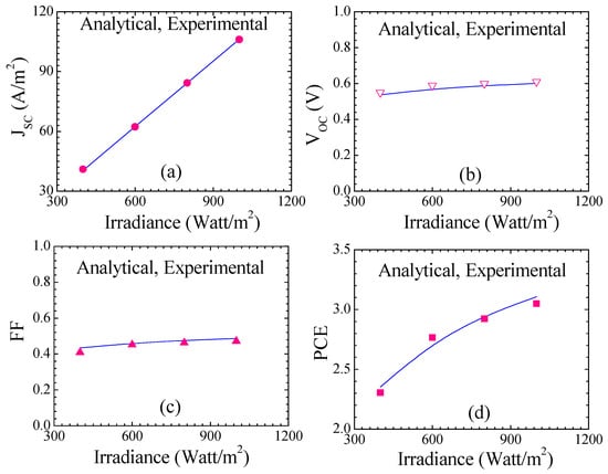
Figure 8.
Analytical (solid line) and experimental (marker) [22] results of short circuit current (JSC), open circuit voltage (VOC), fill factor (FF), and power conversion efficiency (PCE) with the variation of irradiance.
The internal properties (absorbance, EQE, and IQE) of OSC have been analyzed by calculating them by analytical expressions developed earlier. Absorbance has been calculated by using the analytical Equation (62). Average photocurrent has been calculated by using Equation (63) and then EQE by Equation (64) Again, IQE has been evaluated by using absorbance and EQE in Equation (65). These equations provide the result for a single wavelength. Similarly, by calculating internal properties for different wavelengths, the spectral variations of the internal properties have been obtained. Figure 9 shows the spectral variation of absorbance, EQE, and IQE for active layer thickness 100 nm and irradiance 1000 W/m2. The analytical results fully matched with numerical results as shown, this indicates that these analytical equations are correct. For absorbance, the variation pattern and level of values are consistent with the reported results of such devices [34,50,51,52,53,54]. A similar shape is also observed for EQE which is consistent with reported works [6,50,53,54].
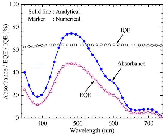
Figure 9.
Spectral variation of absorbance, EQE, and IQE for OSC with the irradiance of 1000 W/m2.
As absorbance and EQE have the almost same shape and IQE = EQE/absorbance, the shape of IQE is almost constant with the wavelength as shown in Figure 9, a similar constant shape of IQE is also observed by others [52].
The effects of variation of active layer thickness on the generation rate of excitons and charge carriers have been investigated as follows. For a certain value of active layer thickness (), exciton generation rate has been calculated by using Equation (18) for a certain position and a certain wavelength; thus calculated for all positions inside active layer and all wavelengths. Then for a certain position, the results of all wavelengths have been integrated to get the effects of all photons; thus, calculated for all positions. Then the results of all positions have been integrated to get total excitons; when the exciton generation rate (unit: s−1m−3) is integrated with the position for the range of 0 to , it gives exciton generation rate per unit area (unit: s−1m−2); this represents the number of excitons generated per unit time in the volume covering a unit area of incident-surface and length of whole active layer thickness. Such calculation of exciton generation rate per unit area has been carried out for several values of . Then charge carrier generation rate per unit area has been calculated by the product of exciton generation rate and dissociation probability. Figure 10 shows the generation rate per unit area versus for both excitons and charge carriers. Both show deep ripples at lower values of and shallow ripples at higher values of . For some , the interaction of incident and reflected light would be additive intensive and hence the generation would be high; whereas, for some , the interaction would be subtractive intensive, and hence the generation would be low; therefore, the ripple. The overall trend of variation is, the exciton (per unit area) increases with , this is because of the large space available for photon absorption. On the other hand, charge carrier = (exciton)(probability). We know, field , for a certain , with the increase of , field decreases, and hence probability decreases. That is, with the increase of , charge carrier has two effects: increasing effect of exciton and decreasing effect of probability; for a large value of these two effects are nullified by each other, and hence charge carrier curve increases at a low rate, that is, almost flat as shown. This result is consistent with the results of current density, photons absorbed, the efficiency with the variation of active layer thickness obtained by other researchers [14,31,32,49].
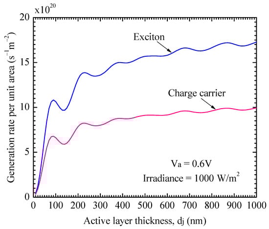
Figure 10.
Generation rate per unit area with the variation of active layer thickness for excitons and charge carriers.
We know, electrons and holes per unit volume is used for calculating the current, therefore, the charge carrier generation rate per unit volume needs to be investigated. As the generation rate per unit area indicates the amount in the volume covering a unit area of incident surface and length of whole active layer thickness, if we divide the generation rate per unit area by the active layer thickness then it will represent the amount in the volume of unit area and unit length, i.e., the average amount in unit volume, thus the average generation rate per unit volume (unit: s−1m−3) has been determined by dividing the generation rate per unit area by , a similar calculation has been done for all values of . Figure 11 shows the generation rate per unit volume versus for both excitons and charge carriers. With the increase of , generation rate per unit volume has two effects: increasing effect of overall generation rate per unit area and decreasing effect due to division by ; at the low range of , increasing effect is more, hence generation rate per unit volume increases; at around 60 nm both effects become equal and the generation rate reaches to maximum, for more than 60 nm, decreasing effect becomes dominant, hence generation rate per unit volume decreases as shown in Figure 11.
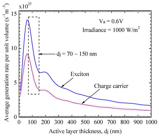
Figure 11.
Generation rate per unit volume versus active layer thickness for excitons and charge carriers.
Some previous work [21] calculated J-V for 70 and 150 nm; some work [25] calculated J-V for 80, 100, 120, and 140 nm; these works showed that current decreases with the increase of ; the present study also supports those previous results because we see that in the similar range (70–150 nm) of , exciton (or charge carrier) generation rate per unit volume decreases with the increase of , which is shown by the box in Figure 11. However, there are some range of for which exciton (or charge carrier) increases with the increase of or remains almost constant as shown in Figure 11, that is, the trend of decreasing current with the increase of would not be true for all range of , that means, this study provides a better and bigger picture regarding the effect of variation of . From this analysis, it is seen that the generation rate per unit volume is the highest for the active layer thickness of 60 nm, therefore, it might be predicted that OSC would provide the highest performance with the active layer thickness of 60 nm. In the literature, we see that many research groups fabricated OSC having an active layer thickness of 100 nm (which is close to 60 nm); may be, they did not go with a lower thickness because of the fabrication challenge.
Maximum power has also been investigated with the variation of active layer thickness; is found to vary with active layer thickness as shown in Figure 12, which has been obtained for irradiance of 1000 W/m2. The variation pattern is similar to that of the charge carrier generation rate per unit volume shown in Figure 11. Charge carrier per unit volume determines the current and hence the power, therefore, the similar shape. For such a device with nm, experimental has been calculated from experimental J-V [22] and plotted along with analytical results; the experimental result matches the analytical result for nm. For calculating analytically with other than 100 nm, the only has been changed keeping all other parameters the same, therefore, we may expect that analytical results with other will also match with the experimental for the same device.
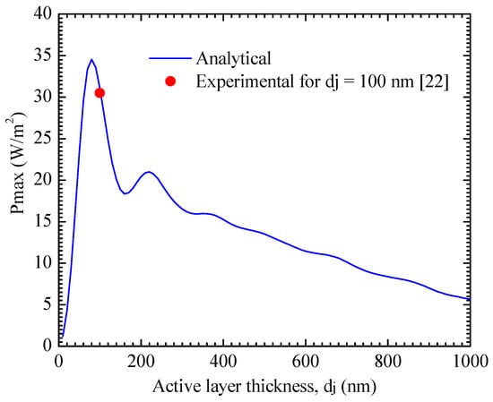
Figure 12.
Variation of maximum power with the variation of active layer thickness with the irradiance of 1000 W/m2.
Comparing with previous work on OSC, this work is expected to provide a better result with a bigger view and clear understanding. This is because this work has been done to shed light on the following matters: (1) detail derivations of analytical expressions of excitons, charge carriers, electrons, holes, current, absorbance, EQE, IQE; (2) investigation of the spatial distribution of excitons inside the active layer of OSC; (3) investigation of separation distance and dissociation probability; (4) improved analytical computation of OSC properties using OTMM-based excitons, SAGD incorporated probability and recombination altogether; (5) investigation of the effects of variation of irradiance on JSC VOC, FF, PCE; (6) spectral analysis of absorbance, EQE, IQE; (7) investigation of the effects of variation of active layer thickness on exciton, charge carrier and .
This work might be utilized for further improvement of OSC, for example, to decide about active layer thickness for obtaining the highest performance. The same calculation approach may be applied to study the optimization of other layer thickness, the replacement of layer materials for the betterment of OSC performances such as the widening of spectral absorption, increasing the efficiency, etc.
7. Conclusions
Photo-generated excitons inside the organic solar cell (OSC) have been calculated using the optical transfer matrix method (OTMM), this shows the pulsating variation with positions inside the active layer having a peak value of 8 × 1027 − 20 × 1027 s−1m−3, due to the effect of optical phenomena. While calculating the charge carriers from excitons, spherically averaged Gaussian distribution (SAGD) incorporated dissociation probability has been found most logical and appropriate. OSC performances have been calculated by analytical equations derived by solving electrical transport equations including OTMM based excitons, SAGD incorporated dissociation probability, and recombination of charge carriers, all together. Analytical results of current producing electrons, holes, J-V, JSC, VOC, FF, PCE, absorbance, EQE, IQE are found to match with numerical and experimental results and consistent with previous works. Exciton and charge carrier generation rate per unit area are found to increase with active layer thickness. Whereas, exciton and charge carrier generation rate per unit volume and Pmax increase, reach to the top and then decrease with active layer thickness; the highest performance at an active layer thickness of 60 nm; these are also found consistent with previous results. The matching of analytical results with numerical results indicates the correctness of analytical expressions, matching with experimental results indicates the capability of predicting OSC properties, and consistency with previous works ensures the validity of the analytical computational results. Compared to previous analytical works on OSC, the results in this work are expected to be more accurate because of including the above-mentioned 3 factors together in the analytical solution. Moreover, calculating OSC performances by the analytical expressions in this work is easy because the expressions are simple and only involves the summation of exponential, sine, and cosine terms. The results of detail analysis are expected to be useful for designing improved OSC and the detailed derivations of analytical expressions are expected to help the readers to understand the OSC research with more insight.
Funding
This work was supported by the Deanship of Scientific Research (DSR), King Abdulaziz University, Jeddah, under grant No. (D-144-135-1438). The author, therefore, gratefully acknowledges the DSR technical and financial support.
Data Availability Statement
Not Applicable.
Acknowledgments
This work was supported by the Deanship of Scientific Research (DSR), King Abdulaziz University, Jeddah, under grant No. (D-144-135-1438). The author, therefore, gratefully acknowledges the DSR technical and financial support.
Conflicts of Interest
The author declares no conflict of interest. The funder had no role in the design of the study; in the collection, analyses, or interpretation of data; in the writing of the manuscript, or in the decision to publish the results.
Appendix A
Let us find and . We may assume, and are the forward and backward field components at the beginning of layer (Figure 1). Here starts from the left boundary (; when it reaches position , it becomes , which is represented by , that is, . Similarly, for the backward direction, starts from the position ; when it reaches the left boundary (, it becomes , which is represented by , that is, that results in . Using the above expressions of and in Equation (7) we get Equation (8).
Appendix B
Let us find and . We may define an internal forward transfer coefficient () as , hence we get . Again, starts from left boundary; when reaches at the right boundary, it becomes ; after reflection at the right boundary, leftward field is ; when reaches at the left boundary, it becomes , which is represented by , that is, , by using we may get, . Putting the above expressions of and in Equation (8) we get Equation (9).
Appendix C
Let us find . Like the Equation (4), and may be related with and via and hence we may get that results . Since or = , therefore, . Using the above expression of we may get the expression of as in Equation (10).
Appendix D
Putting in Equation (11) and assigning , , , we obtain
The absolute value of can be found as
where, .
Appendix E
Irradiance () is the power per unit area. To derive the equation of , we may start with parallel plate capacitor energy and its electric field. Capacitor energy = = = = . Hence, we get, Energy/Volume = . Light with speed , falling on a material having surface area , will provide optical energy to a volume of of the material during time . Energy in a volume = = . Now, Power = = . Then, Irradiance = = .
Appendix F
Now, incident irradiance that results . Again, according to Maxwell, light speed ; where magnetic permeability. For non-magnetic material, , therefore, . Accordingly, and . Again, for such non-magnetic material, the refractive index = = = = = . Accordingly, and , hence = . Using the above relations in Equation (14), we can get Equation (15).
Appendix G
Naturally, the separation distances will be different for different excitons because of the difference in photon energy. Depending on the material used in the device, a specific separation distance would be most feasible and hence the number of excitons with that separation distance would be the highest; for other separation distances the excitons would be less. This phenomenon may be addressed by giving different weights to the probability corresponding to different separation distances by using a standard distribution function of . For this purpose, the spherically averaged Gaussian distribution (SAGD) function may be used and hence the probability may be calculated by Equation (23).
Appendix H
Many researchers found the active layer thickness of 100 nm suitable for making a good performance OSC; constant field assumption works well until 200 nm thickness; therefore, this assumption would be acceptable for most of the available OSC devices. Again, due to the difference in mobility of electron and hole, the charge transport may become unbalanced, as a result, a net space charge may build-up, this space charge may affect the electric field, this effect has been assumed negligible. These assumptions regarding the electric field have been considered to obtain a complete analytical solution. Again, monomolecular recombination has been included because this allows us to obtain a complete analytical solution. The analytical solution would not be possible for bimolecular recombination. In the situation where these assumptions would not be valid, we have to use numerical computation.
Appendix I
The particular solution of the differential Equation (31) is
Using from Equation (25) which is for single wavelength, we obtain
Appendix J
At , electron concentration [12,36]: , where is the effective density of states at PCBM LUMO (≡ conduction band), is the electron injection barrier potential at (see Figure 2b), is the thermal voltage. Applying this boundary condition to Equation (35) we obtain
At the boundary position (), electron concentration depends on electron injection barriers, photoexcitation cannot change this electron injection barrier, that is, electron concentration at the boundary does not depend on photon (). Therefore, the -related part at the right side of Equation (A9) should be equal to zero, and hence the constant part at the right side should be equal to the constant part at the left side. That is,
where, .
At , electron concentration [12,36]: , where = electron injection barrier potential at (see Figure 2b). Applying this boundary condition to Equation (35) we obtain
where,
By solving Equation (A11) and Equation (A17) we get the value of and written in Equation (36) and Equation (37), respectively.
By solving Equation (A14) and Equation (A20) we get the value of and written in Equation (38) and Equation (39), respectively.
Appendix K
If we divide incident irradiance (unit: Wm−2 or Js−1m−2) by photon energy (unit: J) then we will obtain incident photon rate as (unit: s−1m−2); as absorbance would be unitless, we need the absorbed photon with the same unit s−1m−2. Equation (16) gives the absorbed photon rate per unit volume (unit: s−1m−3) for a single wavelength. If we integrate with respect to from 0 to , we will obtain the absorbed photon rate per unit area with the unit s−1m−2, this will represent the number of photons absorbed per unit time in the volume covering a unit area of incident-surface and length of whole active layer thickness.
After calculating we will get the Equation (62).
Appendix L
We should use photocurrent (not dark current) for the calculation of EQE. If we divide photocurrent density (unit: Am−2 or Cs−1m−2) by the charge value of an electron (unit: C) then we will obtain photocurrent-producing charge carrier rate with the unit s−1m−2. Note that, Equation (44) and Equation (58) give the photocurrent density and for a single wavelength. Total photocurrent density is the function of , therefore, the average value is to be calculated, then the photocurrent-producing charge carrier rate can be calculated as .
After calculating we will get the Equation (63).
References
- Krebs, F.C. Fabrication and processing of polymer solar cells: A review of printing and coating techniques. Sol. Energy Mater. Sol. Cells 2009, 93, 394–412. [Google Scholar] [CrossRef]
- Kippelen, B.; Brédas, J.-L. Organic photovoltaics. Energy Environ. Sci. 2009, 2, 251–261. [Google Scholar] [CrossRef]
- Li, G.; Liu, L.; Wei, F.; Xia, S.; Qian, X. Recent Progress in Modeling, Simulation, and Optimization of Polymer Solar Cells. IEEE J. Photovolt. 2012, 2, 320–340. [Google Scholar] [CrossRef]
- Ma, W.; Yang, C.; Gong, X.; Lee, K.; Heeger, A.J. Thermally Stable, Efficient Polymer Solar Cells with Nanoscale Control of the Interpenetrating Network Morphology. Adv. Funct. Mater. 2005, 15, 1617–1622. [Google Scholar] [CrossRef]
- Li, G.; Shrotriya, V.; Huang, J.; Yao, Y.; Moriarty, T.; Emery, K.; Yang, Y. High-efficiency solution processable polymer photovol-taic cells by self-organization of polymer blends. Nat. Mater. 2005, 4, 864–868. [Google Scholar] [CrossRef]
- Green, M.A.; Emery, K.; Hishikawa, Y.; Warta, W.; Dunlop, E.D. Solar cell efficiency tables. Prog. Photovolt. Res. Appl. 2012, 20, 12–20. [Google Scholar]
- Park, S.H.; Roy, A.; Beaupré, S.; Cho, S.; Coates, N.E.; Moon, J.S.; Moses, D.; Leclerc, M.; Lee, K.; Heeger, A.J. Bulk heterojunction solar cells with internal quantum efficiency approaching 100%. Nat. Photon. 2009, 3, 297–302. [Google Scholar] [CrossRef]
- Häusermann, R.; Knapp, E.; Moos, M.; Reinke, N.A.; Flatz, T.; Ruhstaller, B. Coupled optoelectronic simulation of organic bulk-heterojunction solar cells: Parameter extraction and sensitivity analysis. J. Appl. Phys. 2009, 106, 104507. [Google Scholar] [CrossRef]
- Koster, L.J.A.; Smits, E.C.P.; Mihailetchi, V.D.; Blom, P.W.M. Device model for the operation of polymer/fullerene bulk het-erojunction solar cells. Phys. Rev. B Condens. Matter 2005, 72, 1–9. [Google Scholar] [CrossRef]
- Monestier, F.; Simon, J.-J.; Torchio, P.; Escoubas, L.; Flory, F.; Bailly, S.; de Bettignies, R.; Guillerez, S.; Defranoux, C. Modeling the short-circuit current density of polymer solar cells based on P3HT: PCBM blend. Sol. Energy Mater. Sol. Cells 2007, 91, 405–410. [Google Scholar] [CrossRef]
- Sievers, D.W.; Shrotriya, V.; Yang, Y. Modeling optical effects and thickness dependent current in polymer bulk-heterojunction solar cells. J. Appl. Phys. 2006, 100, 114509. [Google Scholar] [CrossRef]
- Kumar, P.; Jain, S.C.; Kumar, V.; Chand, S.; Tandon, R.P. A model for the J-V characteristics of P3HT: PCBM solar cells. J. Appl. Phys. 2009, 105, 104507. [Google Scholar] [CrossRef]
- Marsh, R.A.; McNeill, C.R.; Abrusci, A.; Campbell, A.R.; Friend, R.H. A unified description of current-voltage characteristics inorganic and hybrid photo-voltaics under low light intensity. Nano Lett. 2008, 8, 1393–1398. [Google Scholar] [CrossRef]
- Altazin, S.; Clerc, R.; Gwoziecki, R.; Pananakakis, G.; Ghibaudo, G.; Serbutoviez, C. Analytical modeling of organic solar cells and photodiodes. Appl. Phys. Lett. 2011, 99, 143301. [Google Scholar] [CrossRef]
- Heavens, O.S. Optical Properties of Thin Solid Films; Dover Publications: New York, NY, USA, 1956. [Google Scholar]
- Pettersson, L.A.; Roman, L.S.; Inganäs, O. Modeling photocurrent action spectra of photovoltaic devices based on organic thin films. J. Appl. Phys. 1999, 86, 487–496. [Google Scholar] [CrossRef]
- Chowdhury, M.M.; Alam, M.K. An analytical model for bulk heterojunction organic solar cells using a new empirical expression of space dependent photocarrier generation. Solar Energy 2016, 126, 64–72. [Google Scholar]
- Rahman, M.S.S.; Alam, M.K. Effect of angle of incidence on the performance of bulk heterojunction organic solar cells: A unified optoelectronic analytical framework. AIP Adv. 2017, 7, 1–15. [Google Scholar] [CrossRef]
- Islam, M.; Wahid, S.; Chowdhury, M.M.; Hakim, F.; Alam, M.K. Effect of spatial distribution of generation rate on bulk het-erojunction organic solar cell performance: A novel semi-analytical approach. Org. Electron. 2017, 46, 226–241. [Google Scholar] [CrossRef]
- Ng, A.; Liu, X.; Jim, W.Y.; Djurišić, A.B.; Lo, K.C.; Li, S.Y.; Chan, W.K. P3HT: PCBM solar cells-The choice of source material. J. Appl. Polym. Sci. 2013, 131, 39776. [Google Scholar] [CrossRef]
- Arnab, S.M.; Kabir, M.Z. An analytical model for analyzing the current-voltage characteristics of bulk heterojunction organic solar cells. J. Appl. Phys. 2014, 115, 1–7. [Google Scholar] [CrossRef]
- Liu, L.; Li, G. Investigation of recombination loss in organic solar cells by simulating intensity-dependent current–voltage measurements. Sol. Energy Mater. Sol. Cells 2011, 95, 2557–2563. [Google Scholar] [CrossRef]
- Onsager, L. Initial Recombination of Ions. Phys. Rev. 1938, 54, 554–557. [Google Scholar] [CrossRef]
- Braun, C.L. Electric field assisted dissociation of charge transfer states as a mechanism of photocarrier production. J. Chem. Phys. 1984, 80, 4157–4161. [Google Scholar] [CrossRef]
- Islam, M.S. Analytical modeling of organic solar cells including monomolecular recombination and carrier generation calculated by optical transfer matrix method. Org. Electron. 2017, 41, 143–156. [Google Scholar] [CrossRef]
- Wojcik, M.; Tachiya, M. Accuracies of the empirical theories of the escape probability based on Eigen model and Braun model compared with the exact extension of Onsager theory. J. Chem. Phys. 2009, 130, 104107. [Google Scholar] [CrossRef]
- Hilczer, M.; Tachiya, M. Unified Theory of Geminate and Bulk Electron−Hole Recombination in Organic Solar Cells. J. Phys. Chem. C 2010, 114, 6808–6813. [Google Scholar] [CrossRef]
- Onsager, L. Deviations from Ohm’s Law in Weak Electrolytes. J. Chem. Phys. 1934, 2, 599–615. [Google Scholar] [CrossRef]
- Trukhanov, V.A.; Bruevich, V.V.; Paraschuk, D.Y. Effect of doping on performance of organic solar cells. Phys. Rev. B 2011, 84, 205318. [Google Scholar] [CrossRef]
- Mihailetchi, V.D.; Koster, L.J.A.; Hummelen, J.C.; Blom, P.W.M. Photocurrent Generation in Polymer-Fullerene Bulk Heterojunctions. Phys. Rev. Lett. 2004, 93, 216601. [Google Scholar] [CrossRef]
- Nam, Y.M.; Huh, J.; Jo, W.H. Optimization of thickness and morphology of active layer for high performance of bulk-heterojunction organic solar cells. Sol. Energy Mater. Sol. Cells 2010, 94, 1118–1124. [Google Scholar] [CrossRef]
- Li, G.; Liu, L. Carbon Nanotubes for Organic Solar Cells. IEEE Nanotechnol. Mag. 2011, 5, 18–24. [Google Scholar] [CrossRef]
- Shrotriya, V.; Li, G.; Yao, Y.; Chu, C.-W.; Yang, Y. Transition metal oxides as the buffer layer for polymer photovoltaic cells. Appl. Phys. Lett. 2006, 88, 73508. [Google Scholar] [CrossRef]
- Liang, C.-W.; Su, W.-F.; Wang, L. Erratum: Enhancing the photocurrent in poly(3-hexylthiophene)/[6,6]-phenyl C61 butyric acid methyl ester bulk heterojunction solar cells by using poly(3-hexylthiophene) as a buffer layer. Appl. Phys. Lett. 2009, 95, 219902. [Google Scholar] [CrossRef]
- Cahen, D.; Ginley, D. Fundamentals of Materials for Energy and Environmental Sustainability; Cambridge University Press: Cambridge, UK, 2011; p. 233. [Google Scholar]
- Sze, S.M.; Mattis, D.C. Physics of Semiconductor Devices; John Wiley & Sons: New York, NY, USA, 1970. [Google Scholar]
- Iverson, A.; Smith, D. Mathematical modeling of photoconductor transient response. IEEE Trans. Electron. Devices 1987, 34, 2098–2107. [Google Scholar] [CrossRef]
- Arnab, S.M.; Kabir, M.Z. Modeling of the effects of charge transport on voltage-dependent photocurrent in ultrathin CdTe solar cells. J. Vac. Sci. Technol. A 2013, 31, 061201. [Google Scholar] [CrossRef]
- American Society for Testing and Materials. Solar Spectral Irradiance: Air Mass 1.5. Available online: http://rredc.nrel.gov/solar/spectra/am1.5/ (accessed on 15 March 2020).
- Rad, H.M.; Zhu, F.; Singh, J. Profiling exciton generation and recombination in conventional and inverted bulk heterojunction organic solar cells. J. Appl. Phys. 2018, 124, 1–11. [Google Scholar]
- Chowdhury, M.M.; Alam, M.K. An optoelectronic analytical model for bulk heterojunction organic solar cells incorporating position and wavelength dependent carrier generation. Sol. Energy Mater. Sol. Cells 2015, 132, 107–117. [Google Scholar] [CrossRef]
- Tan, K.-S.; Chuang, M.-K.; Chen, F.-C.; Hsu, C.-S. Solution-Processed Nanocomposites Containing Molybdenum Oxide and Gold Nanoparticles as Anode Buffer Layers in Plasmonic-Enhanced Organic Photovoltaic Devices. ACS Appl. Mater. Interfaces 2013, 5, 12419–12424. [Google Scholar] [CrossRef]
- Hao, Y.; Song, J.; Yang, F.; Hao, Y.; Sun, Q.; Guo, J.; Cui, Y.; Wang, H.; Zhu, F. Improved performance of organic solar cells by incorporating silica-coated silver nanoparticles in the buffer layer. J. Mater. Chem. C 2015, 3, 1082. [Google Scholar] [CrossRef]
- Gasparini, N.; Salvador, M.; Heumueller, T.; Richter, M.; Classen, A.; Shrestha, S.; Matt, G.J.; Holliday, S.; Strohm, S.; Egelhaaf, H.-J.; et al. Polymer: Nonfullerene Bulk Heterojunction Solar Cells with Exceptionally Low Recombination Rates. Adv. Energy Mater. 2017, 7, 1701561. [Google Scholar] [CrossRef]
- Kurpiers, J.; Neher, D. Dispersive Non-Geminate Recombination in an Amorphous Polymer: Fullerene Blend. Sci. Rep. 2016, 6, 26832. [Google Scholar] [CrossRef] [PubMed]
- Nalwa, K.S.; Kodali, H.K.; Ganapathysubramanian, B.; Chaudhary, S. Dependence of recombination mechanisms and strength on processing conditions in polymer solar cells. Appl. Phys. Lett. 2011, 99, 263301. [Google Scholar] [CrossRef]
- Saleheen, M.; Arnab, S.M.; Kabir, M.Z. Analytical Model for Voltage-dependent photo and dark currents in bulk heterojunction organic solar cells. Energies 2016, 9, 412. [Google Scholar] [CrossRef]
- Yeboah, D.; Singh, J. Study of the Contributions of Donor and Acceptor Photoexcitations to Open Circuit Voltage in Bulk Heterojunction Organic Solar Cells. Electronics 2017, 6, 75. [Google Scholar] [CrossRef]
- Khanam, J.J.; Foo, S.Y. Modeling of High-Efficiency Multi-Junction Polymer and Hybrid Solar Cells to Absorb Infrared Light. Polymers 2019, 11, 383. [Google Scholar] [CrossRef]
- Yang, S.; Sun, X.; Zhang, Y.; Li, G.; Zhao, X.; Li, X.; Fu, G. Enhancing the Efficiency of Polymer Solar Cells by Modifying Buffer Layer with N,N-Dimethylacetamide. Int. J. Photoenergy 2014, 2014, 1–6. [Google Scholar] [CrossRef]
- Tembo, M.; Munyati, M.O.; Hatwaambo, S.; Maaza, M. Efficiency enhancement in P3HT: PCBM blends using Squarylium III dye. Afr. J. Pure Appl. Chem. 2015, 9, 50–57. [Google Scholar]
- Yoshida, K.; Okul, T.; Suzuki, A.; Akiyama, T.; Yamasaki, Y. Fabrication and Characterization of PCBM: P3HT Bulk Heterojunc-tion Solar Cells Doped with Germanium Phthalocyanine or Germanium Naphthalocyanine. Mater. Sci. Appl. 2013, 4, 1–5. [Google Scholar]
- Lee, E.J.; Choi, M.H.; Moon, D.K. Enhanced Photovoltaic Properties of Bulk Heterojunction Organic Photovoltaic Devices by an Addition of a Low Band Gap Conjugated Polymer. Materials 2016, 9, 996. [Google Scholar] [CrossRef]
- Ikram, M.; Niaz, N.A.; Khalid, N.R.; Ramzan, M.; Imran, M.; Ali, S. Tetra Blended Based Hybrid Bulk Heterojunction Solar Cells. Materials 2016, 9, 996. [Google Scholar]


Publisher’s Note: MDPI stays neutral with regard to jurisdictional claims in published maps and institutional affiliations. |
© 2021 by the author. Licensee MDPI, Basel, Switzerland. This article is an open access article distributed under the terms and conditions of the Creative Commons Attribution (CC BY) license (http://creativecommons.org/licenses/by/4.0/).