Article

An IoT Device for Autonomous Groundwater Monitoring: Solar Energy Harvesting, Power Management, and LoRa Communication

1
Departamento de Ingeniería Eléctrica y de Computadoras, Universidad Nacional del Sur, ICIC (UNS-CONICET), Bahia Blanca 8000, Buenos Aires, Argentina
2
Instituto Nacional de Tecnologia Agropecuaria Estación Experimental H. Ascasubi (INTA), Hilario Ascasubi 8142, Buenos Aires, Argentina
3
Departamento de Agronomía, Universidad Nacional del Sur, Bahia Blanca 8000, Buenos Aires, Argentina
4
Departamento de Ingeniería Eléctrica y de Computadoras, Universidad Nacional del Sur, LISSI (UNS-CICPBA), Bahia Blanca 8000, Buenos Aires, Argentina
*
Author to whom correspondence should be addressed.
Hardware 2026, 4(3), 16; https://doi.org/10.3390/hardware4030016
Submission received: 5 June 2026 / Revised: 18 July 2026 / Accepted: 27 July 2026 / Published: 3 August 2026

Abstract

Measuring the water table level is a critical factor in irrigated agriculture in arid regions, as it can significantly influence the exchange of water and nutrients with crops. This work presents the design, implementation, and field validation of an open-source, solar-powered IoT device for autonomous groundwater level monitoring, combining long-range low-power LoRa communication, a non-contact pressure-based level sensor using the trapped-air capillary method, and an efficient power management stage that seamlessly switches between solar and battery power. Unlike existing commercial leveloggers, which are costly and lack integrated wireless telemetry and solar-based autonomy, the proposed platform is presented as a fully open-source, low-cost alternative purpose-built for unattended deployment in areas without grid power or cellular coverage. The system was validated through a multi-day field trial and dedicated communication tests, demonstrating a stable power conversion efficiency of 84–90%, a five-day autonomous operation without any deep-discharge event, high linearity ( R 2 = 0.9998) of the level module over a 0–2 m range with a resolution of approximately 1.94 mm per ADC count, and a reliable LoRa link of up to 8.51 km in an urban/suburban environment despite non-line-of-sight conditions. With an estimated hardware cost of approximately $100 USD per unit, the device represents a low-cost, low-maintenance tool capable of generating knowledge about water resources to optimize irrigation and crop management in the face of climate change.

1. Introduction

Sustainable Smart Cities (SSC) deploy intelligent systems that contribute to improving the quality of life of their inhabitants and provide solutions for socio-economic development while prioritizing the conservation of natural resources [1]. In this model, sensor networks under the Internet of Things (IoT) paradigm play a crucial role, providing real-time information that must be properly processed to prevent environmental events and provide support to planning decisions [2].
One of the application areas is precision agriculture, where improved operational dynamics have been achieved, as these IoT-based tools facilitate decision-making for producers [3,4]. For example, when crop production relies on the implementation of canal irrigation systems that distribute water from rivers and drainage ditches, these systems, while conveying water, also contribute to the underground system and alter the soil environment [5,6,7]. Regional topography and soil physical properties are relevant factors in the characteristics of the environment influenced by the water table, since, depending on where the capillary zone is located, water can rise to the roots of the crop. Previous research indicates that when the water table is near the surface (<5 m), it favors the exchange of water and nutrients with the soil and vegetation, and can be a source of water for crops [8]. Obtaining a real-time record of these seasonal and occasional rises in water levels is very important to understand how this aquifer recharge can be influenced by both water inputs during the irrigation season and by precipitation, and also whether these factors contribute to crop development.
The scenario in which these sensor networks are deployed is complex. The challenges of covering large areas with diverse topographies, with limited or no access to electricity supply, along with poor antenna coverage for cellular networks (3G, 4G LTE, or 5G) demand technological solutions to develop sensor networks that are economical to implement and maintain, have low energy consumption, wide range and coverage, and the ability to interconnect a large number of devices. Currently, communication devices that meet these constraints are available for implementing low-power wide area networks (LPWANs). Among the most widely used are LoRa and Sigfox [9,10], which operate in unlicensed space. LoRa has the advantage of inexpensive transceivers and a wide variety of IoT devices that count with them.
Several efforts have been made to implement data networks for water resource monitoring, aiming for low-cost and real-time solutions to improve groundwater management, thus overcoming the limitations of traditional methods. In this sense, Kombo et al. [11] implemented a low-cost system in Zanzibar using encapsulated pressure sensors for underwater applications. Communication between nodes and the gateway was carried out using LoRaWAN, and the gateway connected to the Internet via GPRS/GSM (4G LTE).
Espinoza Ortiz et al. [12] developed a low-cost IoT system to monitor piezometric level and temperature of groundwater. Sensors were linked to an ESP8266 microcontroller with WiFi.
Calderwood et al. [13] proposed a low-cost and scalable sensor network for monitoring groundwater. The WSN used pressure transducers and Solinst Leveloggers/LevelSenders telemetry units that transmitted data via a cellular network to a local server.
Drage and Kennedy et al. [14] created a community-based network in Nova Scotia with custom water level meters. These IoT devices (using ultrasonic sensors) transmitted data to the Internet via WiFi or cellular connection to the ThingSpeak platform for real-time visualization and delivery of warnings. Similarly, Malche and Maheshwary et al. [15] proposed an IoT prototype for water level monitoring, using an Arduino Uno board, with an Ethernet shield for Internet connectivity.
Although these proposals focus on reducing costs and enable real-time monitoring, none of them offers a network to be deployed in places where there is no GPRS/GSM (4G LTE) connectivity, as required in many Latin American rural areas and the costs of these proposals are still high. The proposal reported in this paper provides a solution for groundwater monitoring by considering these contexts and significantly reducing costs.
The main contribution of this work is the design and implementation of an open-source hardware and software IoT device for measuring groundwater levels, with the potential to expand the number of sensors. The design includes not only the development of a reliable and low-cost sensor for measuring groundwater levels, but also a comprehensive analysis of the power system based on a solar panel and rechargeable battery to achieve an autonomous and low-maintenance device. The information generated and processed by the IoT device will allow for the development of knowledge about fluctuations in the water table and the quality of the groundwater resource, and consequently, the generation of proposals for irrigation and crop management. These actions help mitigate the main problems associated with climate change that arid and semi-arid regions face in agricultural production. This work is the result of a collaborative project between the National University of the South and the National Institute of Agricultural Technology (INTA). To the authors’ knowledge, no similar embedded design instrument exists in the academic field.

2. Design Overview

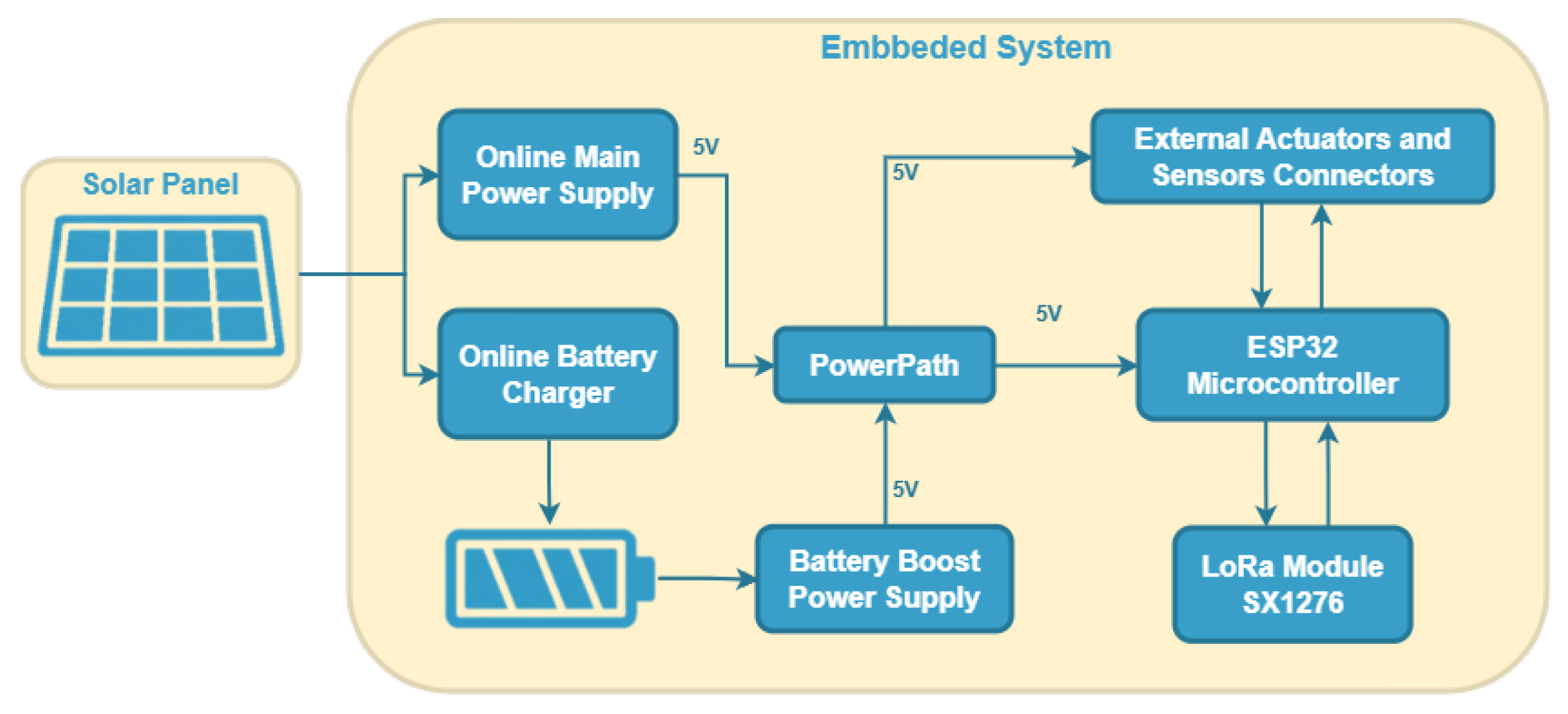
The proposed embedded system is a solar-powered, self-contained sensing node designed for autonomous field deployment. As illustrated in Figure 1, the system harvests energy from a photovoltaic solar panel, which simultaneously feeds a Main Power Supply and a Battery Charger that maintains a dedicated battery. To ensure uninterrupted operation, a PowerPath switching stage seamlessly selects between the regulated solar supply and a Battery Boost Power Supply—the latter converting the battery voltage up to the system’s 5 V bus when solar energy is unavailable. The conditioned 5 V rail powers the core of the embedded system: an ESP32 microcontroller, which manages data acquisition through a set of sensors that can be added through the External Actuators and Sensors Connectors, and communicates wirelessly over long-range, low-power links via an SX1276 LoRa module. This architecture guarantees continuous operation across day/night cycles and variable irradiance conditions, making the node well-suited for remote monitoring applications where grid power is inaccessible.
The selection of the LTC3130, LT3652, and LTC4412 integrated circuits over other commercially available solutions was guided by a consistent set of design criteria: circuit simplicity, favoring parts requiring a minimal external component count and analog control over solutions requiring a microcontroller and dedicated firmware; compliance with the system’s voltage, current, and power requirements as dictated by the solar panel and battery specifications; cost, given the target of a low-cost, deployable sensing node and, critically, the availability of vendor-supplied SPICE models, which allowed each candidate to be simulated and validated under realistic operating conditions before committing to a physical design. For the Main Power Supply stage, alternatives such as Analog Devices’ LTC3119 and LTC3105, and Texas Instruments’ BQ25570 and TPS63070 families were considered; these were discarded either for lacking an integrated MPPC-like input clamping function, for offering lower efficiency at the system’s power levels, for not reaching system’s voltage, current, and power requirements, or for the absence of a usable SPICE model. For the Battery Charger, competing solar-charging solutions such as Texas Instruments’ BQ24650 and BQ25504, and the CN3791 (a widely used low-cost solar charge controller), were evaluated; these were ultimately not selected due to a combination of higher external component count, less straightforward MPPT-threshold programming, and, in the case of the CN3791, the lack of an accurate SPICE model suitable for the simulation workflow adopted in this work. For the PowerPath switching stage, alternatives such as Analog Devices’ LTC4359 and Texas Instruments’ TPS2115A/TPS2121 PowerPath controllers were considered, but the LTC4412 was preferred for its lower pin count, simpler biasing, and well-documented SPICE model, consistent with the minimal-BOM philosophy adopted across the power management subsystem.
Regarding MPPT, classical algorithms such as Perturb and Observe (P&O) or Incremental Conductance actively perturb the operating point and track power in real time, which requires a microcontroller with dedicated voltage/current sensing and firmware. This conflicts with the design philosophy adopted for the power management stage of this system, in which the charging path is kept entirely analog and free of microcontroller supervision: actively measuring current and voltage to run such algorithms would add sensing hardware and control complexity, demanding more from the design and increasing overall system cost. Weighed against this added complexity, the resulting gain in energy-harvesting efficiency was considered insufficient to justify the trade-off for this application. For this reason, integrated circuits implementing a fixed-voltage MPPT scheme were selected, allowing the hardware to remain simple and low-cost while still achieving decent harvesting performance, resulting in a design built around the LTC3130 and the LT3652. A fixed-voltage MPPT scheme exploits the fact that the MPP voltage of a given solar panel varies only weakly with irradiance and temperature, so a single setpoint, programmed with a simple resistor divider, approximates the MPP closely enough in practice while requiring no active control loop or additional sensing hardware. This approach sacrifices some tracking precision under fast-changing irradiance conditions compared with P&O or Incremental Conductance, but was considered an acceptable trade-off given the cost and power budget targeted for this system; the implementation details of this mechanism are presented in the following sections.

2.1. MCU Selection

The ESP32 was selected as the central processing unit of the embedded system on the basis of its broad feature set relative to its cost. The device integrates a dual-core Xtensa LX6 processor, a 12-bit successive-approximation ADC, a built-in DAC, Wi-Fi and Bluetooth connectivity, and a rich set of digital peripherals [16]—all in a single, widely available package—making external conversion or communication ICs unnecessary for the majority of the system’s acquisition and control tasks.
The integrated 12-bit ADC provides 4096 quantization levels across the configurable input range (up to 3.3 V in the ADC_ATTEN_DB_11 attenuation mode) [17], which was found to be more than sufficient for the signal chain described in this work. As shown in Section 2.6.8, the pressure-sensor signal occupies a span of approximately 1105 counts out of 4096, yielding a theoretical height resolution of 1.81 mm / count —a level of precision comfortably adequate for the target application without requiring an external ADC.
From a software perspective, the ESP32 is natively supported by the Espressif IoT Development Framework (ESP-IDF) [18], which ships with a port of FreeRTOS [19,20] as its real-time operating system kernel. This was a decisive factor in the MCU selection: FreeRTOS allows the firmware to be structured as a set of concurrent, prioritized tasks—sensor acquisition, power management, LoRa transmission—while the built-in tickless idle mode and the ESP32’s hardware sleep states (light sleep and deep sleep) [21] can be exploited transparently to minimize mean current consumption between measurement cycles. Designing a real-time, low-power system on a platform where the RTOS and the power-management API are both first-class citizens of the official SDK substantially reduces firmware complexity and risk.
The ESP32 also exposes a sufficient number of GPIO pins for all required interfaces: the ADC input from the level sensor module, the SPI bus to the SX1276 LoRa module, the enable line for the sensor power switch, and any auxiliary status or debugging signals. Espressif provides actively maintained, well-documented driver libraries for all of these peripherals [18], which shortens development time and improves long-term maintainability.
Finally, the cost advantage of the ESP32 over functionally comparable alternatives (e.g., STM32 series, nRF52840, or dedicated LoRa-integrated MCUs) was significant. At the time of design, the DEVKITV1 module was available for under $5 USD, making it an exceptionally cost-effective choice for a system that already demands a non-trivial power management subsystem, a LoRa radio, and environmental sensors.

2.2. Solar Panel LTSpice Model

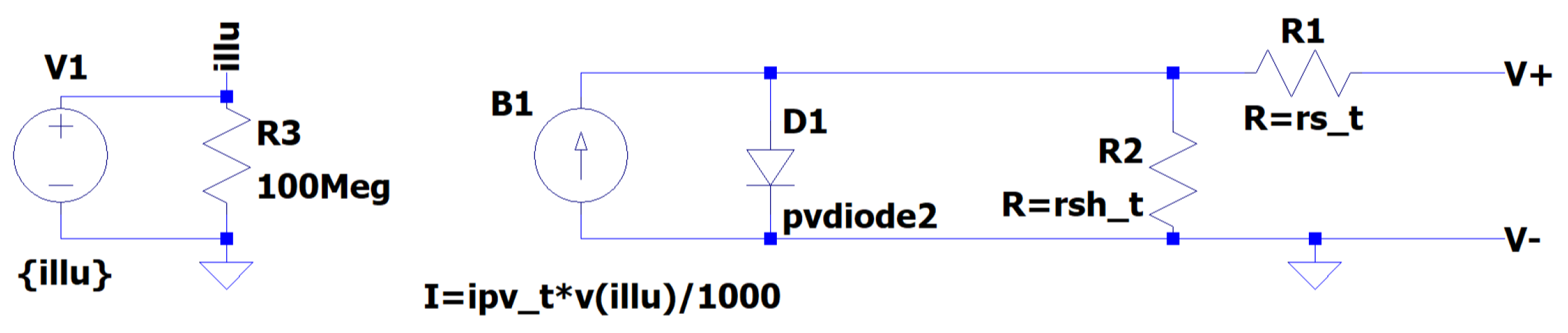
This work uses an LTSpice photovoltaic (PV) module macro-model based on the classical single-diode equivalent circuit, which represents the module as a light-generated current source in parallel with a diode and a shunt resistance ( R s h ), plus a series resistance ( R s ) at the terminals. This structure captures the main non-idealities observed in commercial PV modules: (i) ohmic losses in the interconnects and contacts (modeled by R s ), (ii) leakage paths and recombination effects (modeled by R s h ), and (iii) the exponential IV behavior of the p–n junction (modeled by the diode). The model is implemented with a voltage-controlled current source (for the photocurrent), a diode model, and explicit series/shunt resistors, so it can be directly reused as a drop-in power source when simulating downstream circuits (e.g., rectifiers, battery chargers, and power-path controllers). It is displayed in the Figure 2.
The parameter identification follows analytical expressions reported in the literature, with the goal of requiring only standard datasheet values (open-circuit voltage V O C , short-circuit current I S C , and the maximum power point coordinates V M P and I M P ), while also allowing temperature-dependent operation through the manufacturer-provided temperature coefficients. In particular, the model is aligned with approaches that compute R s , R s h and diode parameters from datasheet points and then validate the resulting curves by comparing the simulated IV and PV characteristics against expected behavior across operating conditions [22,23,24].
To account for temperature variations, the four key datasheet points are first corrected from the reference condition (typically 25   ° C ) using the voltage and current temperature coefficients. In the LTSpice implementation, the temperature-adjusted values are computed as V O C , t , I S C , t , V M P , t and I M P , t , which are then used to estimate the internal resistances. The series resistance is approximated from the separation between V O C , t and V M P , t , while the shunt resistance is derived from the difference between I S C , t and I M P , t . Although these expressions are approximations, they provide a practical and robust starting point for circuit-level simulations when detailed manufacturer parameters are not available.
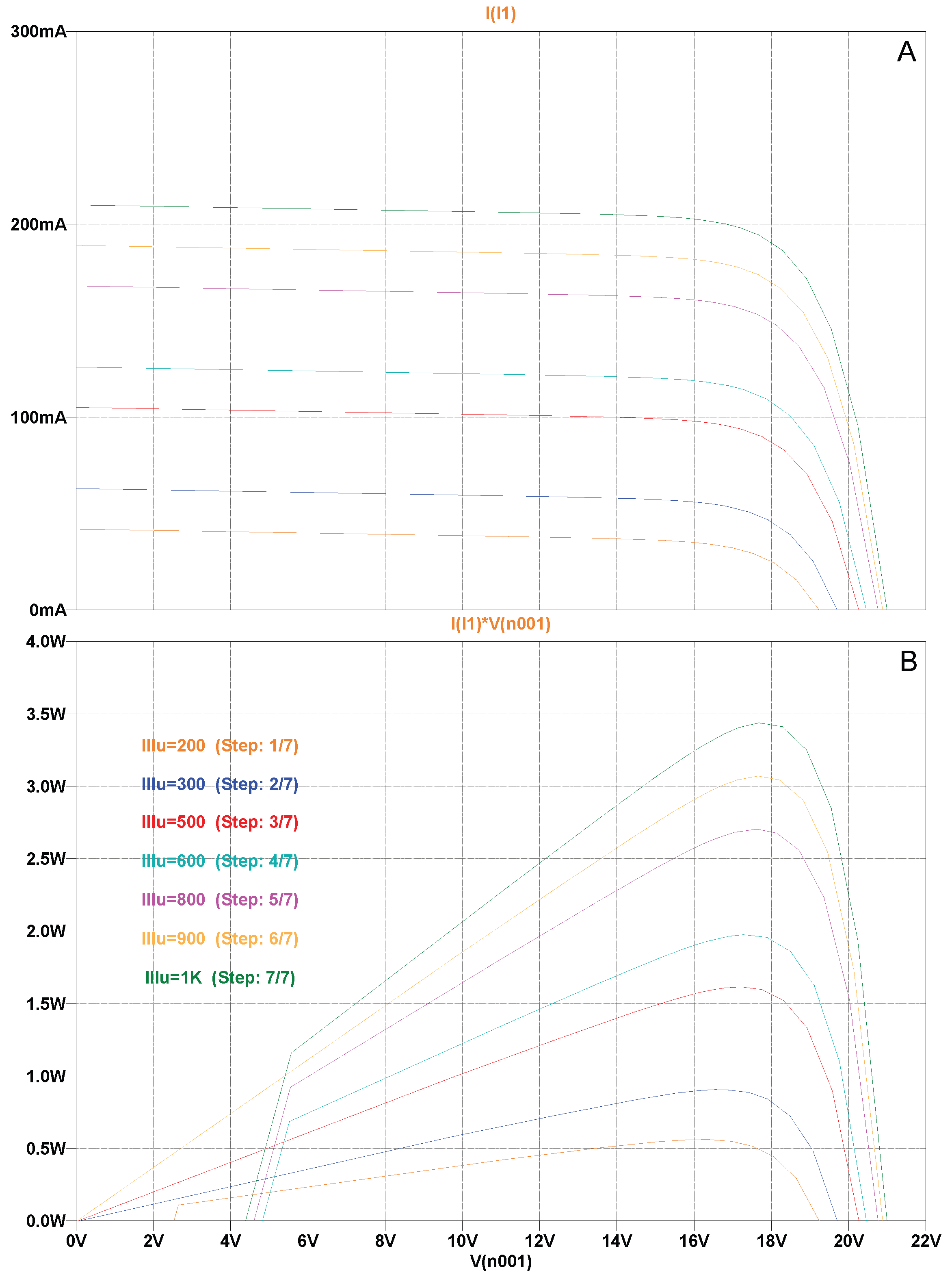
The diode reverse saturation current I o is obtained by enforcing the open-circuit condition of the equivalent circuit at V O C , t , and the diode ideality factor a n is chosen to match the curvature typically observed in commercial modules. The thermal voltage term V t , t is computed from Boltzmann’s constant and the simulated temperature, and the light-generated current I P V , t is scaled so that the short-circuit condition is satisfied. Together, these steps produce a PV macro-model whose terminal behavior reproduces the expected IV knee and the maximum power point specified by the datasheet, as seen in Figure 3.
For clarity and reproducibility, the LTSpice parameter set is included below. The first block defines the temperature-adjusted quantities and the extracted model parameters. The second block lists the commercial (datasheet) parameters used as inputs for a representative module. These blocks can be copied directly into an LTSpice netlist or into a schematic as Spice directives (see Listings 1 and 2).
Listing 1. LTSpice directives for the single-diode PV macro-model (parameter extraction and temperature scaling).
{.param voc_t  voc*(1-tk_voc*(25-temp))
.param isc_t  isc*(1-tk_isc*(25-temp))
.param vmp_t  vmp*(1-tk_voc*(25-temp))
.param imp_t  imp*(1-tk_isc*(25-temp))
.param rs_t   (voc_t-vmp_t)/(16*imp_t) ; 2 instead of 16 in original source
.param rsh_t  5*vmp_t/(isc_t-imp_t)    ; 1 instead of 5 in original source
.param io_t   ((rs_t+rsh_t)*isc_t-voc_t)/(rsh_t*exp(voc_t/(a_n*vt_t)))
.param vt_t   (1.38e-23*(273+temp))/1.6e-19
.param ipv_t  isc_t*(rsh_t+rs_t)/rsh_t
.param a_n    1.3*voc/0.7
.model pvdiode2 d(Is=io_t N=a_n Tnom=temp)}
Listing 2. Commercial (datasheet) parameters used as inputs to the LTSpice PV macromodel.
{.param voc=21.6
.param isc=0.34
.param vmp=17
.param imp=0.29
.param tk_voc=-0.0037
.param tk_isc=0.065}

2.3. Main Power Supply Source

The energy harvested from the photovoltaic module is inherently variable: the open-circuit voltage of the SOLARTEC KS3T panel spans roughly from 10 V to 22 V across its full temperature and irradiance range, while the 5 V output for the system should remain stable to prevent the microcontroller from resetting and entering a corrupt state or failing. A linear regulator is, therefore, unsuitable as the system power supply, since any input variation would be translated to the 5 V output; also, any voltage drop across its pass transistor would dissipate a fraction of the already-limited harvested energy as heat. Instead, a monolithic synchronous buck-boost switching converter—the LTC3130 from Analog Devices—was selected to accept the full V I N range and regulate a stable output voltage regardless of whether the input is above, below, or equal to V O U T .

2.3.1. IC Architecture and Selection Rationale

The LTC3130 operates in average current-mode control with a fixed 1.2 MHz switching frequency, achieving a peak efficiency of 95% and sustaining an ultra-low quiescent current of 1.6 μ A in Burst Mode®, which is critical when the system remains in a low-power standby state between measurement cycles. Its wide input range (2.4 V to 25 V) covers all expected operating points of the solar source, and its integrated Maximum Power Point Control (MPPC) function prevents the input rail from collapsing under high-impedance source conditions—like, for example, a solar panel under low irradiance conditions which is a characteristic failure mode when directly coupling a PV module to a converter without source impedance compensation [25].
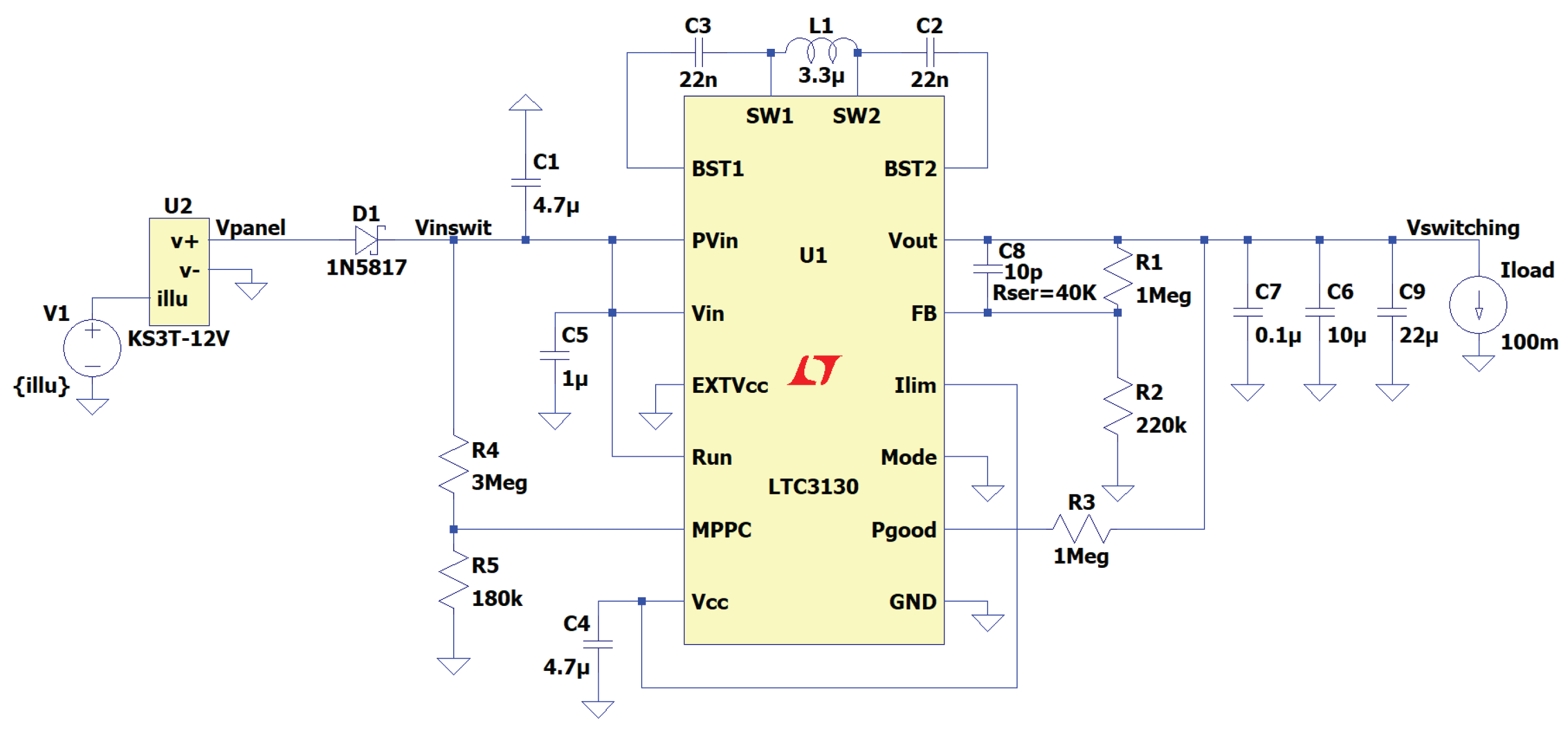
The implemented circuit is shown in Figure 4. It comprises the LTC3130 in a standard application with a single power inductor, input and output bulk capacitors, and two external resistor dividers: one for output voltage programming and one for MPPC threshold programming.

2.3.2. MPPC Input Voltage Programming

The MPPC pin is driven by an internal transconductance ( g m ) amplifier that compares the divided-down V I N against an internal 1.00 V reference and adjusts the converter’s switching duty cycle to prevent the input from falling below the programmed threshold V I N ( MPPC ) . This soft-clamps the operating point of the PV source near its maximum power point rather than allowing the converter to draw excessive current and collapse the panel voltage. The threshold is set by the resistor divider ( R 4 over R 5 ) according to
V I N ( MPPC ) = 1.00 V · 1 + R 4 R 5
For the SOLARTEC KS3T module, the datasheet maximum power point voltage at standard test conditions (25 °C, 1000 W m−2) is V M P = 17 V [26]. A widely adopted rule of thumb for silicon PV modules sets the MPPC threshold at approximately 80% of the open-circuit voltage, which yields 0.80 × 21.6 V 17.3 V. After analyzing the solar panel Nominal Power Voltage and some verification in the simulation, the value for V I N ( MPPC ) was defined as V I N ( MPPC ) = 17.5 V , substituting it into Equation (1) gives a required ratio R 4 / R 5 = 16.5 . Selecting R 4 = 3 M Ω yields R 5 = 181 k Ω 180 k Ω , which can be realized with standard E96 series values and produces a new acceptable ratio R 4 / R 5 = 16.66 .

2.3.3. Power Inductor and Capacitor Selection

The power inductor was selected as L = 3.3 μ H . At the 1.2 MHz switching frequency and for the expected input and output voltage range, the peak-to-peak inductor current ripple Δ I L in buck mode is bounded by
Δ I L = V O U T L · f S W · 1 V O U T V I N
which, for the worst-case condition V I N 2 V O U T (50% duty cycle), simplifies to Δ I L = V O U T / ( 4 L f S W ) . A larger inductance reduces ripple at the cost of a slower transient response and a larger physical component; 3.3 μ H was found to provide an acceptable balance between ripple attenuation and PCB footprint given the JLC PCB manufacturing constraints.
Input and output bulk capacitors were sized to limit voltage ripple to within 1% of the nominal rail. The input capacitor suppresses the high-frequency current drawn from the source during each switching cycle, which is particularly important when the PV panel—a high-impedance, slowly responding source—is directly connected to V I N . Output capacitors were selected with low equivalent series resistance (ESR) to minimize high-frequency voltage spikes at the load.

2.3.4. LTSpice Simulation and Iterative Tuning

The complete converter circuit, including the PV macro-model described in Section 2.2, was implemented in LTSpice to verify the design under realistic source conditions. Component values—particularly the MPPC divider, the compensation network, and the output capacitance—were iteratively adjusted in simulation until three performance criteria were simultaneously satisfied: (i) stable regulation of the buck/boost converter output voltage ( V s w i t c h i n g ) across the full irradiance range, (ii) acceptable startup transient with no overshoot beyond the output rating, and (iii) converging steady-state efficiency above 90% at the nominal load point.
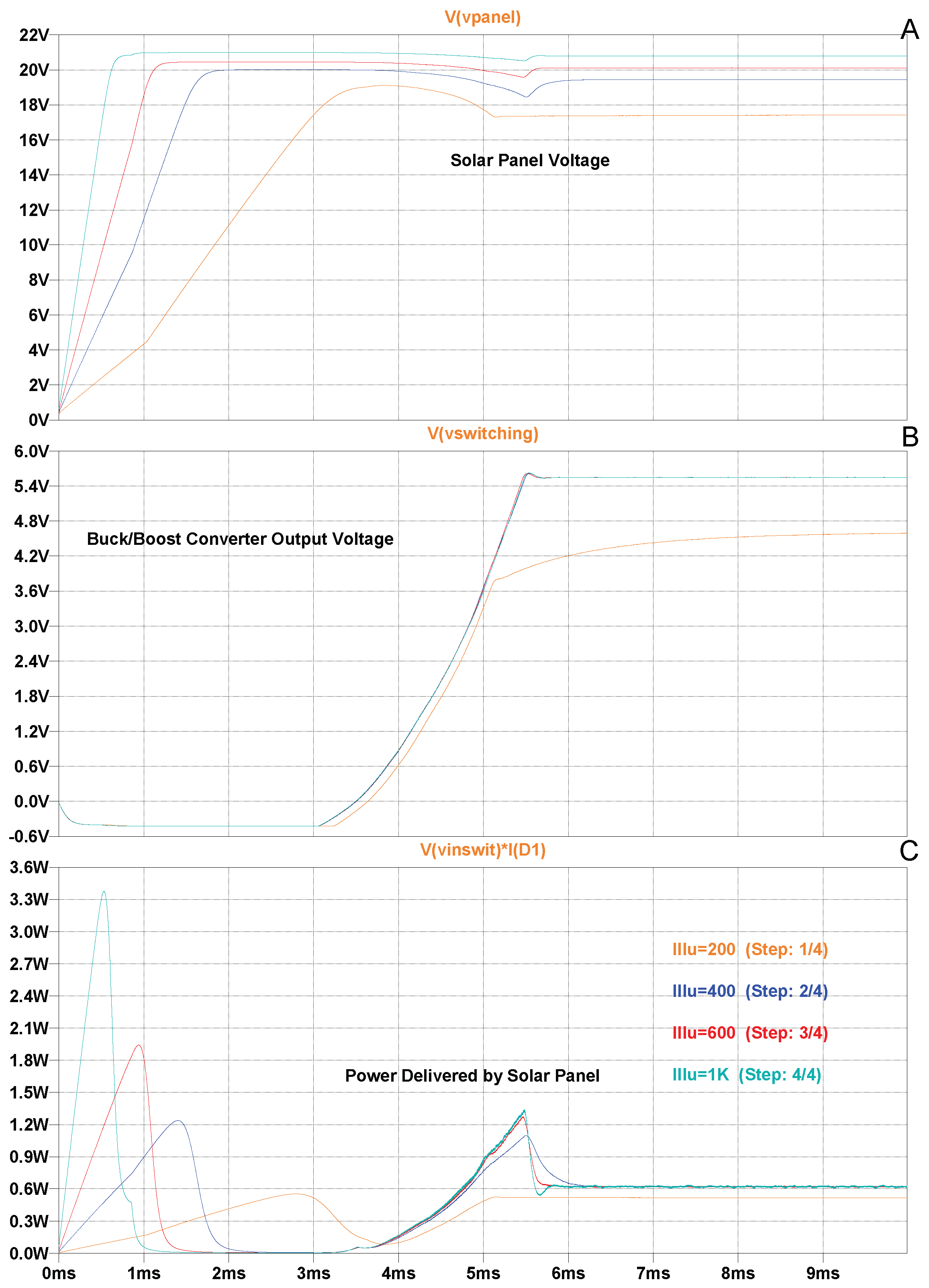
Figure 5 shows the simulated startup response under different illumination conditions for a load current of I l o a d = 100 mA. The output rail rises monotonically to the regulated value without exhibiting underdamped oscillation, confirming that the compensation network is adequately phase-margined. The simultaneous traces of the solar panel output voltage and the converter voltage output ( V s w i t c h i n g ) demonstrate that the converter tracks its input, according to the MPPT setpoint configured and the solar panel output preventing it from collapsing when the illumination is very low. This allows the converter to keep the solar panel at its Maximum Power Point, harvesting the maximum amount of energy possible at each moment (without taking into account solar angle tracking). At irradiance levels of 400 W/m−2 and above, the panel voltage (subplot A) settles above the MPPC threshold of 17.5 V—between 19 V and 21 V—indicating that the MPPC loop is not actively clamping the operating point under these conditions and the panel operates freely above its MPP voltage. At 200 W/m−2, however, the panel voltage stabilizes near 17–18 V, close to the programmed threshold, revealing that the MPPC is actively regulating the converter duty cycle to prevent the panel from collapsing. As a direct consequence, the converter output (subplot B) fails to reach the 5 V setpoint at this irradiance level, settling instead at approximately 4.6 V. This defines a practical minimum irradiance threshold below which full output regulation cannot be maintained. The power transient visible in subplot C during the first millisecond corresponds to an inrush charging spike of the input bulk capacitor: the peak delivered power reaches approximately 3.3 W at 1000 W/m−2 and scales proportionally with irradiance, after which it collapses and recovers to the steady-state value of approximately 1.2 W for all cases above 400 W m−2.
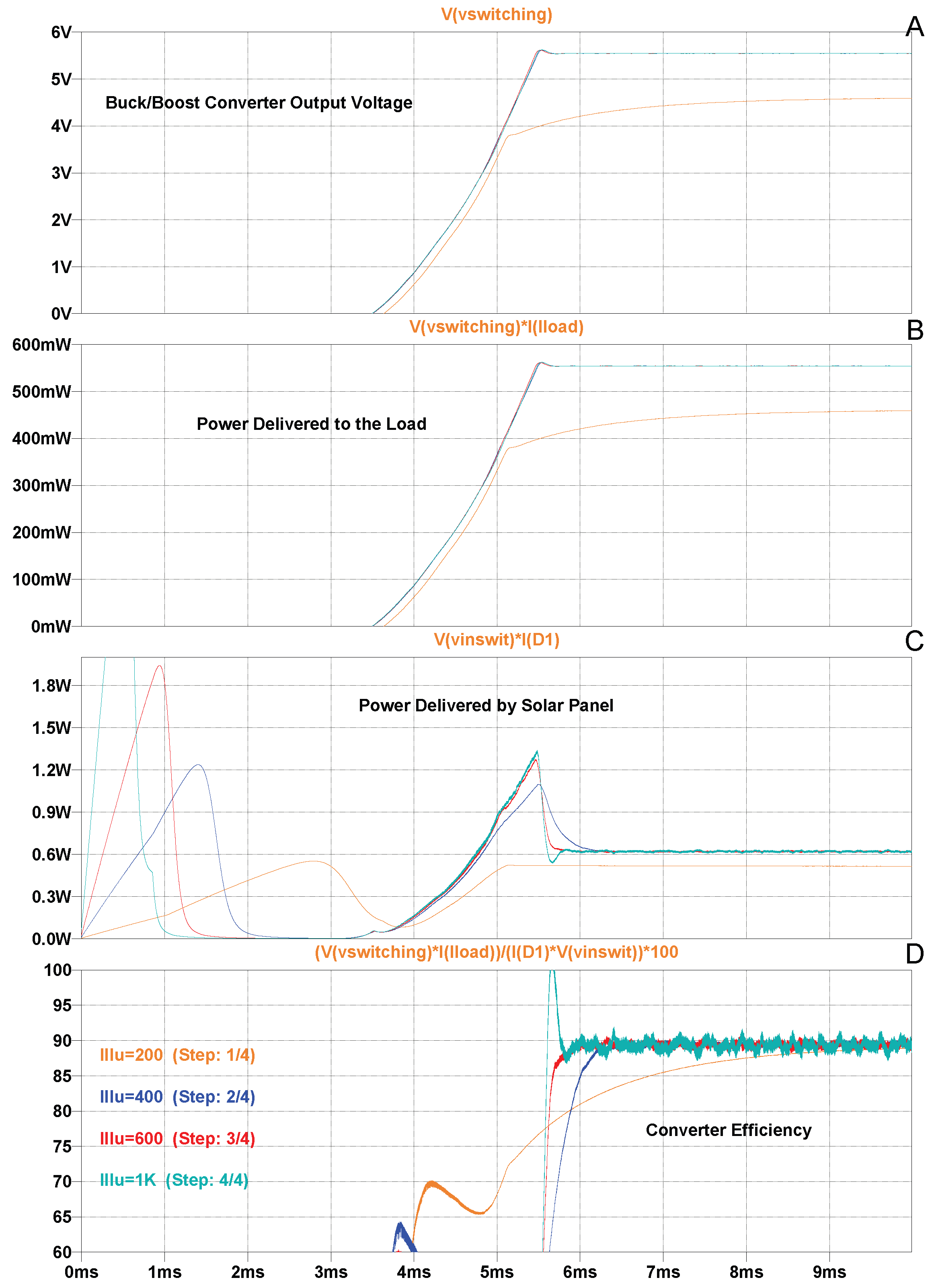
Figure 6 allows for a similar analysis to Figure 5 but from a power efficiency point of view, showing the simulated power and efficiency startup response under different illumination conditions for a load current of I l o a d = 100 mA. The efficiency subplot D provides a direct validation of design criterion (iii): for all irradiance levels at or above 400 W/m−2, the converter converges to a steady-state efficiency between 85% and 90% after the startup transient. During the startup phase (approximately 4–6 ms), efficiency passes through a transient dip to roughly 45–55%; this is expected behavior, as the output capacitors are still charging and the converter operates far from its optimal duty cycle. At 200 W/m−2 the steady-state efficiency is notably lower at the beginning, around 87% (reaching later almost 90% too), consistent with the partial-regulation condition observed in Figure 5. This irradiance level, therefore, also fails to meet design criterion (iii), further confirming it as the practical lower operating boundary of the design.
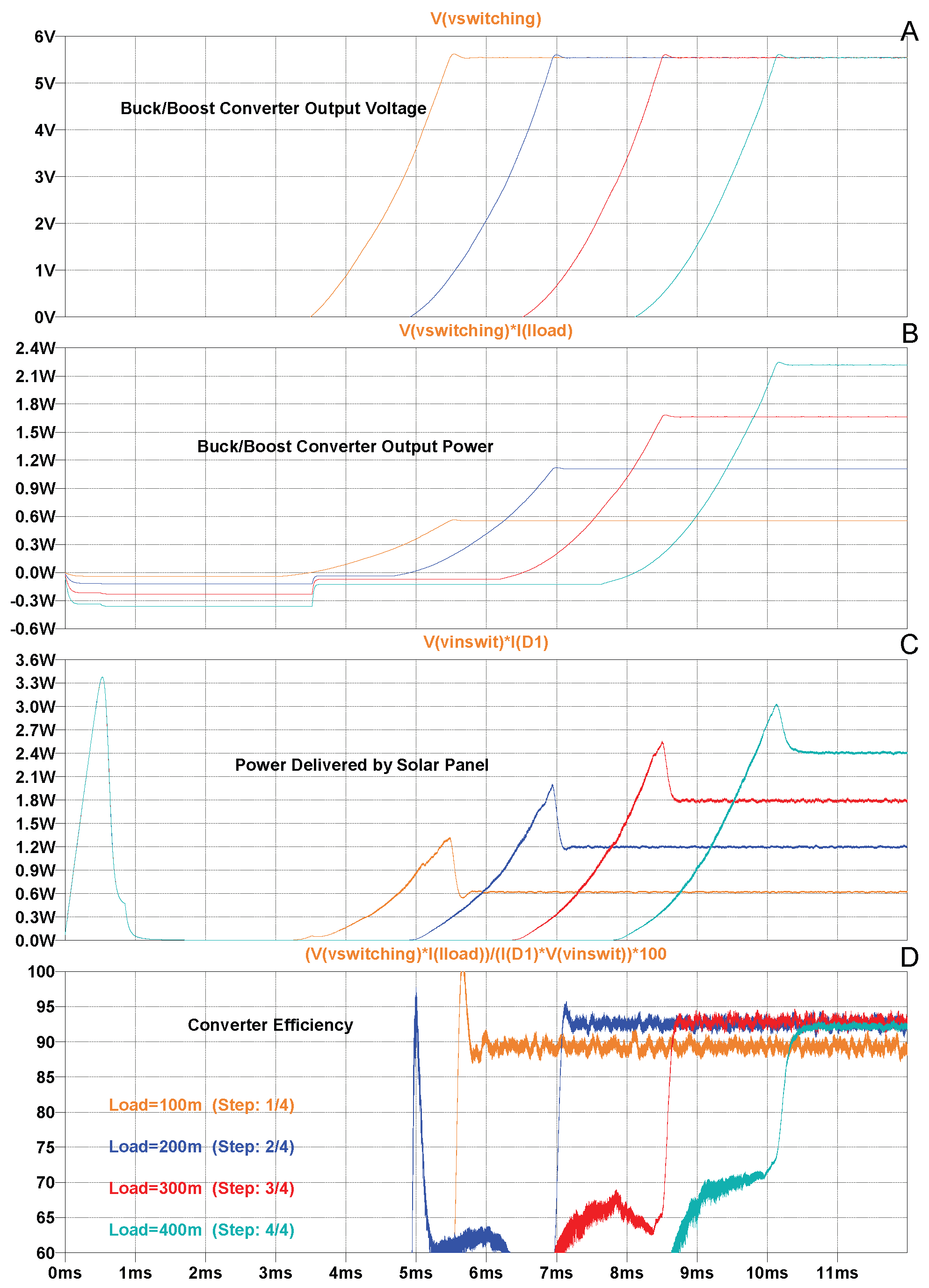
Figure 7 shows a startup response from the converter for different I l o a d values; this allows observation of the converter’s behavior under different output power demands during the startup sequence. Illumination is optimal for all cases (1000 W/m−2). The startup time increases measurably with load: the output rail reaches the 5 V setpoint in approximately 5.5 ms at I l o a d = 100 mA, extending to roughly 7 ms, 8.5 ms, and 10 ms for 200 mA, 300 mA, and 400 mA, respectively. This behavior is consistent with the longer time required for the converter to charge the output capacitance against a heavier discharge current. Notably, despite this variation in startup duration, it is possible to observe that the converter takes more time to start up, but in all the scenarios it managed to deliver the 5 V required output for all loads. The efficiency subplot D reveals a particularly important result: once steady state is reached, the converter maintains approximately 90% efficiency across the entire load range from 100 mA to 400 mA. This load-independent efficiency is a characteristic advantage of the average current-mode controlled topology and confirms that the design remains within its high-efficiency operating region across the full expected system load range. The solar panel power traces in subplot C scale correctly with the load demand—from approximately 0.6 W at 100 mA to approximately 2.4 W at 400 mA—and in all cases remain well below the panel’s peak power capability at full irradiance, confirming that the MPPC is not limiting the operating point under these conditions.
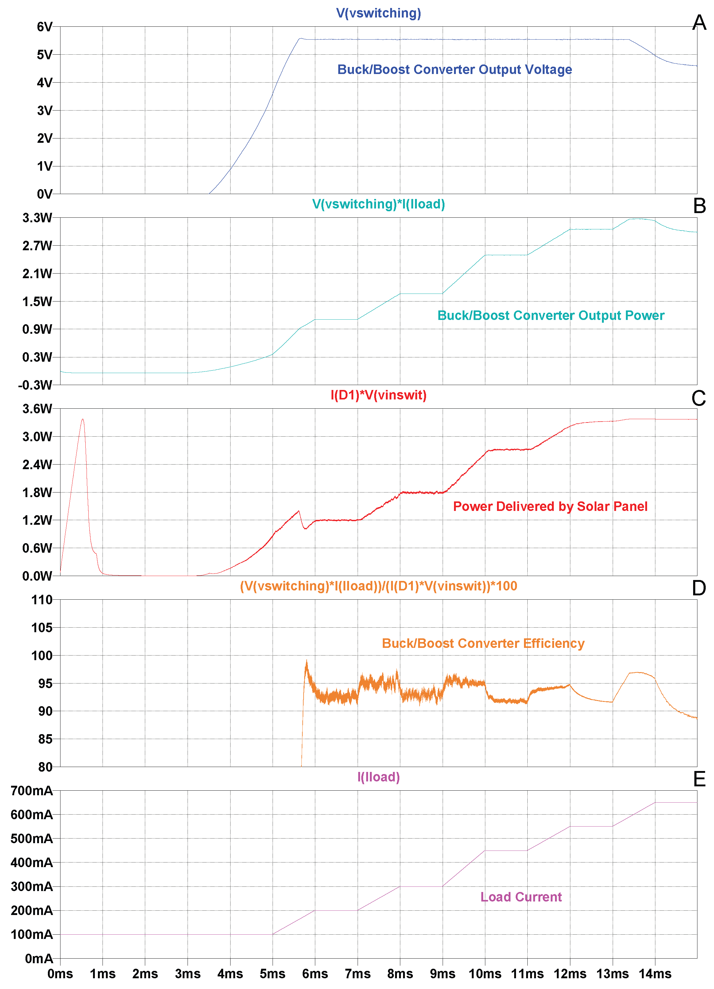
Figure 8 presents the converter behavior under a progressively increasing load current ramp from 100 mA to approximately 600 mA over a 15 ms window, deliberately exceeding the converter’s rated output current to characterize its overload response. As the load current rises toward and beyond the 600 mA buck-mode output current rating (subplot E), the output voltage (subplot A) droops gradually from the regulated 5 V down to approximately 4.6 V. This droop is the expected consequence of the converter’s internal average current limit: the LTC3130 clamps the average inductor current at approximately 850 mA typical, which translates to a maximum output current of approximately 600 mA in buck mode ( I O U T 0.9 · I L ). Once this ceiling is reached, the converter can no longer satisfy the load demand while maintaining regulation, and the output voltage droops rather than the inductor current increasing further. Crucially, the solar panel power (subplot C) rises steadily throughout the entire load ramp without any sag or collapse, confirming that the MPPC function is not active and the panel operating point is not constrained—the bottleneck is the converter’s own current limit, not the source. Furthermore, because the load current at this operating point is well above the Burst Mode transition threshold, the converter has automatically reverted to continuous fixed-frequency PWM operation, as specified by the datasheet; the current limiting behavior observed here is, therefore, identical to that of standard PWM mode. At the maximum simulated load, the converter delivers approximately 3.0 W to the load (subplot B) while drawing approximately 3.3 W from the panel (subplot C), yielding a conversion efficiency of approximately 90% (subplot D)—consistent with the datasheet peak efficiency specification and with the results observed in the startup sweeps. This result confirms that the efficiency target of design criterion (iii) is maintained even as the converter approaches its output current limit.
These simulation results collectively validate the design: the use of a switching converter topology—rather than a linear regulator—maximizes the utilization of the harvested solar energy by maintaining high conversion efficiency across the full operating range of the source, which is essential given the constrained power budget of a remote, solar-only IoT node. In particular, the three design criteria are confirmed: (i) the buck/boost converter output voltage remains stably regulated across the full irradiance range for loads within the panel’s power budget; (ii) the startup transient is monotonic and free of underdamped oscillation across all tested load and irradiance combinations and (iii) steady-state efficiency converges to 85–90% for all operating points above the minimum irradiance threshold of approximately 400 W m−2.

2.4. Battery Charger

The battery charger subsystem is responsible for harvesting energy from the solar panel and delivering it safely to a single-cell 3.3 V lithium-ion battery. The core of the charger is the LT3652 (Analog Devices/Linear Technology), a complete monolithic step-down battery charger IC that operates over a 4.95 V to 32 V input voltage range, making it inherently compatible with the solar panel output range, whose output spans roughly 10 V to 22 V. The LT3652 implements a 1 MHz constant-frequency, average-current-mode step-down architecture, providing a constant-current/constant-voltage (CC/CV) charge profile with a maximum charge current that is externally programmable via a single sense resistor.

2.4.1. Circuit Description

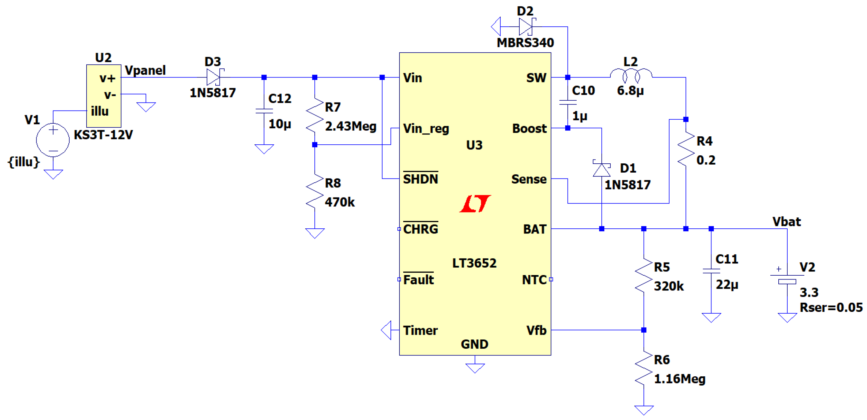
The implemented LTSpice simulation circuit is shown in Figure 9. The solar panel model (block U2) is connected through a reverse-blocking Schottky diode (D3) to the V I N pin of the LT3652 (U3). The MPPT resistor divider (R7 and R8) is connected from V I N to the V I N _ R E G pin, programming the charger’s input voltage regulation setpoint as described in the following section. The SHDN pin is tied to V I N through R8 so that the charger is always enabled when the panel delivers sufficient voltage.
On the output side, the classical buck converter output network consists of inductor L2 and output capacitor C11, with the bootstrap capacitor C10 connected between the BOOST and SW pins via a catch diode (D1), and the freewheeling diode (D2) returning the switch node to V I N . The sense resistor R4 is placed between the SENSE and BAT pins to program the maximum charge current. The battery float voltage is set by the resistor divider R5 and R6 connected from BAT to the VFB pin. The battery model V2 (with R s e r ) represents the nominal lithium-ion cell. The TIMER pin is left open (C/10 termination mode), the NTC pin is pulled to ground through R5, and the CHRG and FAULT open-collector outputs are available for status monitoring.

2.4.2. Charge Current Programming

The maximum charge current is set by the sense resistor R S E N S E (R4) according to the relation given by the LT3652 datasheet:
R S E N S E = 0.1 V I C H G ( M A X )
With R S E N S E = 0.2 Ω , Equation (3) yields
I C H G ( M A X ) = 0.1 V 0.2 Ω = 0.5 A
This value was chosen to balance charging speed against the current capability of the solar panel under typical irradiance conditions. The LT3652 automatically reduces the charge current if the panel voltage falls toward the MPPT setpoint, so the converter never forces the panel below its maximum power point regardless of the battery state of charge.
When the battery is deeply discharged (below 70% of the float voltage), the LT3652 enters a precondition mode in which the charge current is automatically reduced to 15% of I C H G ( M A X ) , i.e., approximately 75 mA, protecting the cell from excessive current while its voltage is very low. Once the battery reaches 70% of the programmed float voltage, full CC charging at 500 mA resumes automatically.

2.4.3. Battery Float Voltage Programming

The LT3652 employs an internal 3.3 V float voltage reference at the VFB pin, so the desired battery float voltage V B A T ( F L T ) is programmed via the R5–R6 resistor divider according to the following:
V B A T ( F L T ) = 3.3 V · R 6 R 6 2.5 × 10 5 Ω
With R5 = 320 k Ω and R6 = 1.16 M Ω :
V B A T ( F L T ) = 3.3 V × 1.16 M Ω 1.16 M Ω 250 k Ω = 3828 k Ω · V 910 k Ω = 4.206 V 4.2 V
The 0.5% reference accuracy of the LT3652 ensures that the programmed float voltage is maintained to within ±20.5 mV, well within the tolerance required to avoid overcharging.
Charge termination is configured in C/10 mode (TIMER pin left open). The charger ends a charge cycle when the current falls to one-tenth of I C H G ( M A X ) , i.e., 50 mA, corresponding to a sense voltage of 10 mV across R4. Once terminated, the LT3652 enters a low-current standby mode (quiescent current 85 μ A) and automatically re-engages charging if the battery voltage drops 2.5% below V B A T ( F L T ) (i.e., below ≈3.998 V), which robustly handles self-discharge between charge sessions.

2.4.4. MPPT Input Voltage Regulation

A key feature of the LT3652 is its input voltage regulation loop, which prevents the solar panel from collapsing under heavy charge demand. The V I N _ R E G pin is driven by a resistor divider from V I N ; the IC servos the charge current downward whenever the V I N _ R E G pin falls below its internal 2.7 V reference, effectively clamping the panel at a programmed minimum voltage. This mechanism implements a fixed-voltage MPPT: the panel is prevented from dropping below the setpoint V I N _ R E G ( M I N ) , which is selected to coincide with the panel’s maximum power point voltage.
The setpoint is given by the following:
V I N _ R E G ( M I N ) = 2.7 V · 1 + R 7 R 8
With R7 = 2.43 M Ω and R8 = 470 k Ω :
V I N _ R E G ( M I N ) = 2.7 V · 1 + 2.43 M Ω 470 k Ω 2.7 V × 6.17 16.66 V
This setpoint of 16.66 V is deliberately placed slightly below the LTC3130 MPPC threshold of 17.5 V (Section 2.4). This ordering is intentional and critical for the overall energy management strategy: because the LT3652 begins to regulate its input before the LTC3130 asserts its MPPC clamp, the battery charger always has priority access to the available panel power. Whenever the panel produces sufficient power, the LT3652 charges the battery first; only after the charger has satisfied its demand (or the panel voltage recovers above 17.5 V) does the LTC3130 freely draw power for the system load. This ensures that the battery is charged opportunistically at every available solar window, even under partial shading or suboptimal irradiance conditions, maximizing the energy stored in the battery over the course of a day.

2.4.5. Simulation Results

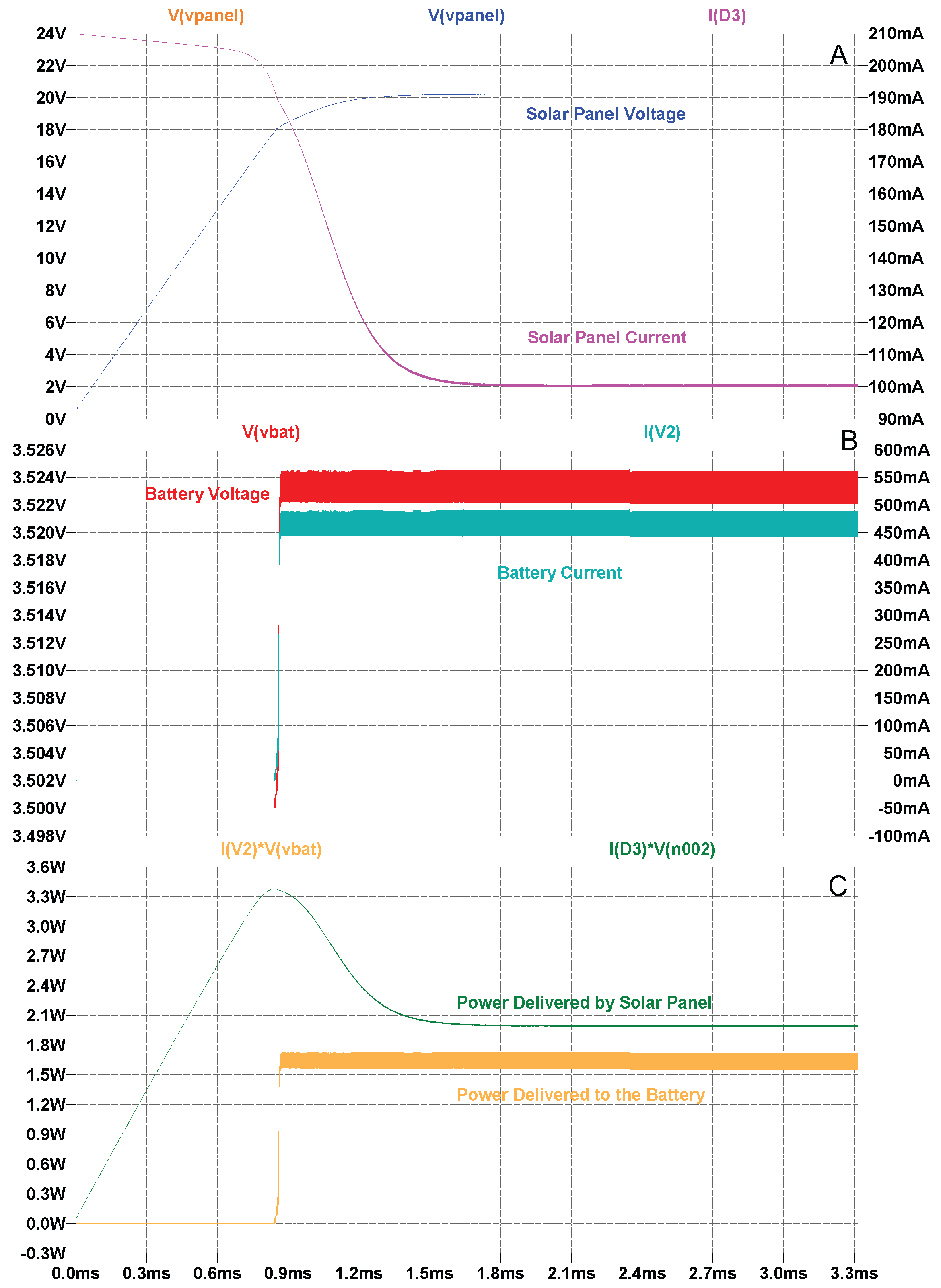
Figure 10 shows the simulated startup transient of the charger. Subplot A displays the solar panel voltage (blue, left axis) and the panel output current (pink, right axis). Subplot B shows the battery voltage (red) and battery current (cyan). Subplot C presents the power delivered by the solar panel (green) and the power delivered to the battery (orange).
At t = 0 , the panel voltage rises from zero as the illumination ramp starts. During the first 0.7 ms, the panel voltage increases gradually and the LT3652 has not yet reached its operational threshold; neither current nor power is delivered to the battery. At approximately t 0.9 ms, the panel voltage crosses the LT3652 startup threshold and the charger engages the following: the battery current abruptly rises to the programmed maximum of ≈500 mA and the battery voltage steps upward from 3.500 V (its initial open-circuit value) to the CC-phase operating point of ≈3.523 V for this occasion (this test was performed assuming a partially charged battery). Concurrently, the power delivered to the battery settles to ≈1.65 W and remains stable thereafter. The solar panel power peaks during the capacitor inrush phase (reaching ≈3.3 W at t 0.7 ms) and then stabilizes near 2.0 W in steady state. The MPPT loop regulates the panel to its programmed 16.65 V setpoint only if necessary; for this case, MPPT is not active as the panel is at full power, reaching approximately 20.0 V; meanwhile, the panel current settles to approximately 100 mA. This startup behavior demonstrates clean, monotonic engagement of the charger without any undesirable oscillation or voltage overshoot at the battery.
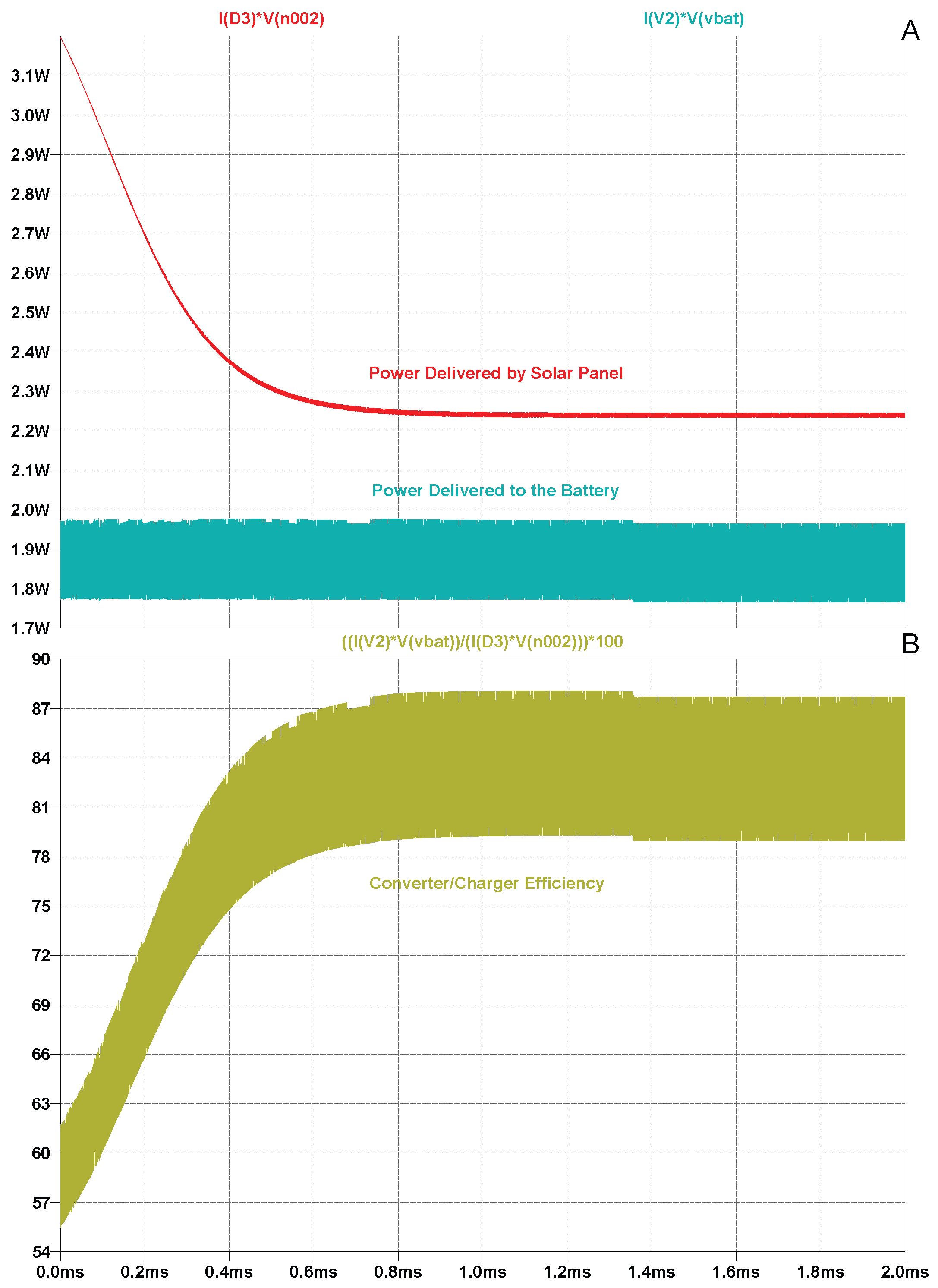
Figure 11 presents the efficiency analysis for a fixed load current of 400 mA into the 3.3 V lithium-ion battery. Subplot A overlays the solar panel delivered power (red) and the battery received power (cyan). Subplot B shows the instantaneous converter/charger efficiency computed as ( P B A T / P p a n e l ) × 100 % .
The panel power decreases monotonically from approximately 3.2 W at t = 0 toward a steady-state value of ≈2.25 W as the MPPT loop brings the panel to its regulated operating point. The power delivered to the battery is remarkably stable at ≈1.8–1.95 W throughout the simulation window, demonstrating that the CC loop effectively rejects the input power variation. The instantaneous efficiency rises from ≈50% at startup—when the panel is far from its regulated point and switching losses dominate—and converges asymptotically to a mean value of ≈84% in steady state. The spread visible in the efficiency waveform corresponds to the 1 MHz switching ripple.
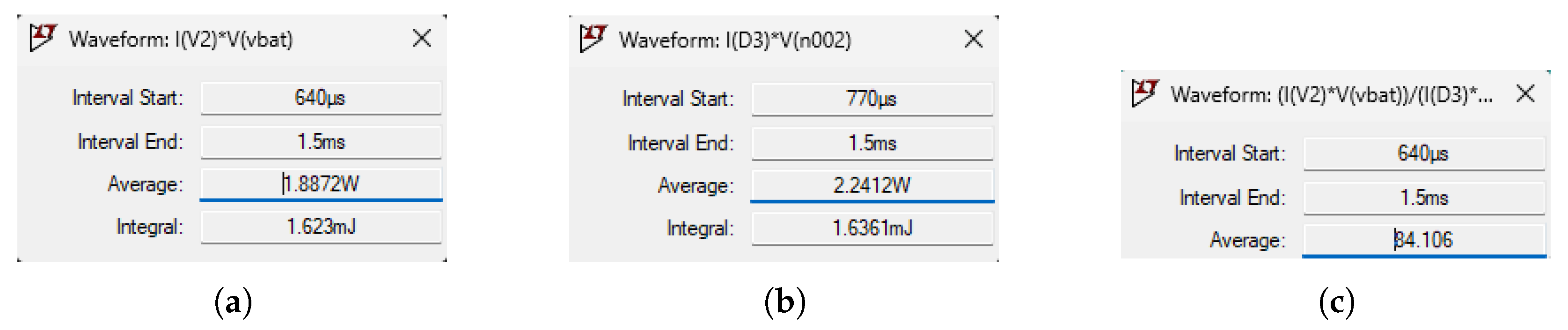
The average values computed by LTSpice over the steady-state interval of Figure 11 are summarized in the measurement panels shown in Figure 12: the average power delivered by the solar panel is 2.2412 W (Figure 12b), the average power transferred to the battery is 1.8872 W (Figure 12a), and the average efficiency is 84.1% (Figure 12c).
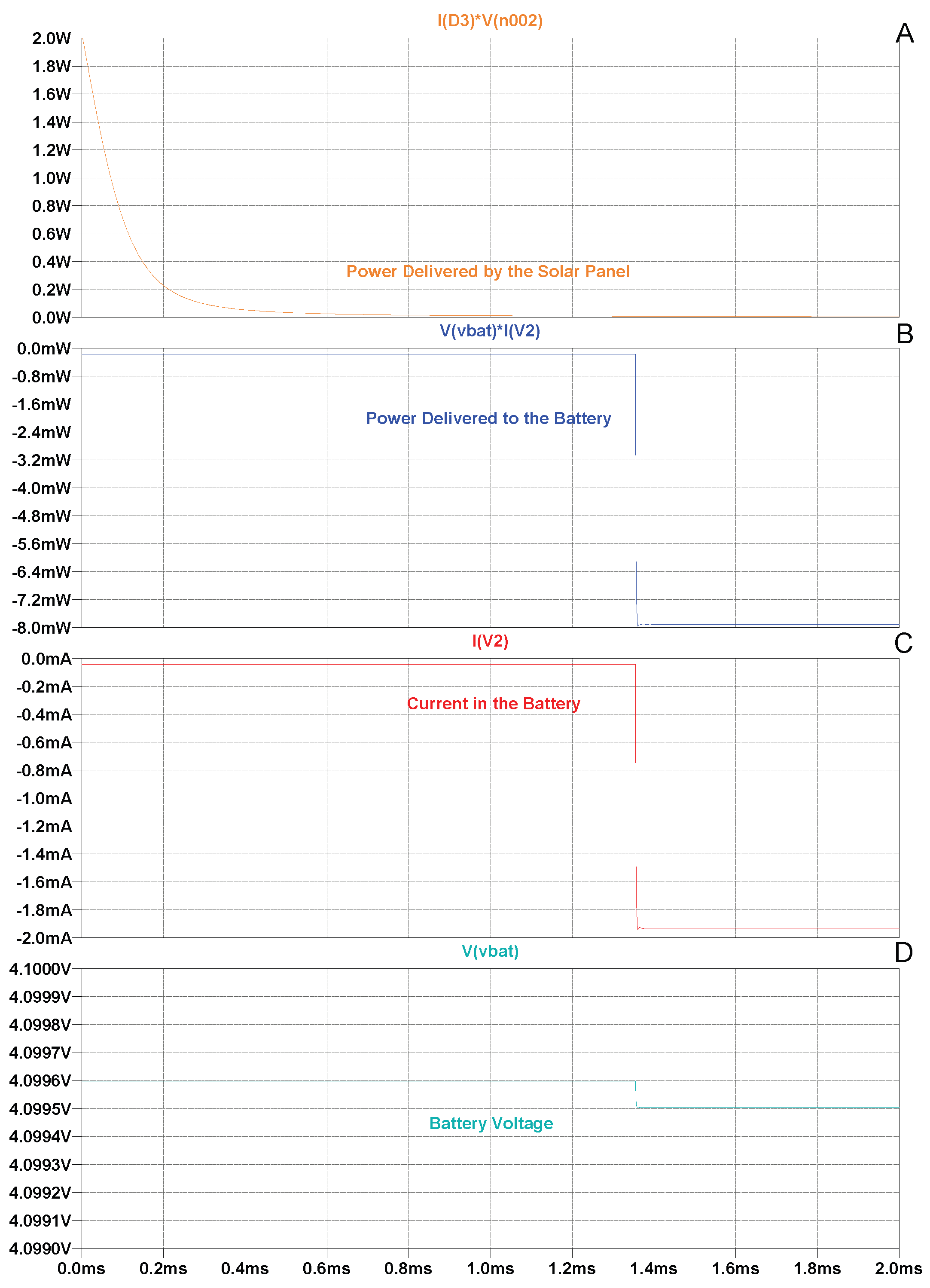
Figure 13 shows the termination sequence as the battery approaches its programmed float voltage of 4.1 V. The simulation is run for a battery nearly fully charged, so the charge current has already tapered well below the full CC value. Subplot A shows the solar panel delivered power (orange); subplot B shows the power delivered to the battery (blue); subplot C shows the battery current (red) and subplot D shows the battery voltage (cyan).
During the interval from 0 to ≈1.35 ms, the panel supplies a small but decreasing power (≈2 W tapering to near zero) while the battery current and delivered power remain essentially at zero—indicating that the charger is already in the final stages of the CV phase with the current approaching the C/10 threshold. At t 1.3 ms, the LT3652 detects that the charge current has fallen under the 50 mA threshold ( I C H G ( M A X ) / 10 ) and terminates the charge cycle: the battery current drops abruptly to approximately −2 mA (the very small LT3652 BAT pin reverse leakage current, well within the specified <0.1 μ A in standby, with the residual here attributable to the simulation model), the battery power swings slightly negative as the charger disengages, and the battery voltage settles to its open-circuit value of ≈4.0995 V—marginally below the float setpoint due to the battery’s internal resistance drop. The solar panel power simultaneously collapses to zero as the charger enters its 85 μ A standby mode and ceases to draw significant current. This behavior confirms the correct operation of the C/10 termination mechanism and the clean transition to standby, with no voltage overshoot or current transient at cutoff.
The simulation results collectively confirm that the LT3652-based charger satisfies the design requirements: (i) the charge current is correctly programmed to 500 mA by R S E N S E = 0.2 Ω ; (ii) the battery float voltage is accurately regulated at 4.1 V via the R5–R6 divider; (iii) the MPPT setpoint at 16.65 V ensures that the solar panel is always operated at or above its maximum power point from the charger’s perspective, and below the LTC3130 MPPC threshold so that battery charging takes priority over the system load; (iv) the charger achieves an average steady-state efficiency of 84.1% at 400 mA charge current and (v) the C/10 termination correctly disengages charging once the battery is full, and the LT3652 returns to its low-power standby mode awaiting the next recharge event.

2.5. PowerPath Circuit Design and Simulation

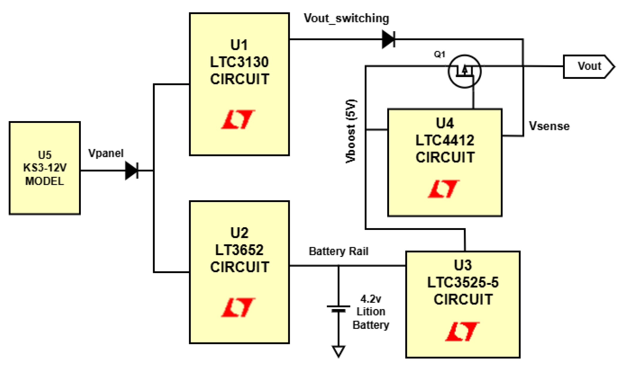
The power management stage of the solar-harvesting system must arbitrate between two competing energy sources—the solar panel output conditioned by the upstream Buck/Boost converter, and the backup energy-storage element while minimizing conduction losses and preserving the integrity of the output voltage rail. The schematic of the complete PowerPath stage is available in the Supplementary Materials, while a simplified schematic is displayed in Figure 14. The solar panel model (U5) feeds the LTC3130 (U1), whose regulated output is presented to the primary input of the LTC4412 PowerPath controller (U4) through a Schottky diode and the P-channel MOSFET (Q1). The battery is charged by the LT3652 charger (U2) and simultaneously boosted to 5 V by the LTC3525-5 (U3), whose output ( V b o o s t ) is connected to the secondary input of the LTC4412. The PowerPath output ( V O U T ) drives a simulated load (current source I l o a d ).

2.5.1. LTC4412 Ideal Diode Controller

Source arbitration is performed by the LTC4412 Low-Loss PowerPath™ Controller [27], a six-pin ThinSOT device that drives an external P-channel MOSFET to implement a near-ideal diode function. In conventional power-OR circuits, a Schottky rectifier introduces a forward voltage drop V f w d on the order of 200 400 mV at moderate currents, resulting in a power dissipation P D = V f w d · I l o a d that scales unfavorably with load. The LTC4412 eliminates this limitation by actively regulating the gate of the external MOSFET so that the drain-to-source voltage is held to V f w d 20 mV during conduction [27], reducing the dissipated power by more than an order of magnitude relative to a Schottky solution for the same current. The relationship between forward voltage and load current for both approaches is fundamentally different: whereas a Schottky diode operates at a nearly constant forward voltage (constant-voltage model), the LTC4412-controlled MOSFET behaves as a constant resistance R O N , yielding V f w d = I l o a d · R D S ( o n ) and a dissipation that remains proportionally small throughout the operating range.
The controller’s quiescent current is I q = 11 μ A (typical), independent of load, making it negligible in the context of the system power budget. Its wide operating range— 2.5 V to 28 V on the battery input and 3 V to 28 V on the auxiliary input—comfortably encompasses the voltage swing produced by the Buck-Boost stage under all illumination conditions. An internal gate-clamp circuit protects the external MOSFET from over-voltage on the gate, and the STAT output pin provides a logic-level flag that a microcontroller can interrogate to determine whether the primary (solar) or secondary (battery) source is currently supplying the load.
From a system-design perspective, the LTC4412 solution is compelling for three additional reasons. First, no sense resistor or current-measurement circuitry is required; the SENSE pin is connected directly to the output (load) node, and source switchover is triggered automatically when the auxiliary voltage exceeds the primary by 20 mV . Second, the part requires only a single bypass capacitor and a pull-up resistor on the STAT line, minimizing bill-of-materials cost and PCB area. Third, the transition between sources is seamless and glitch-free: the MOSFET body diode conducts briefly during the hand-off interval, preventing any interruption of supply to the load before the controller asserts full gate drive.

2.5.2. Circuit Simulation and Behavioral Validation

Two simulation scenarios were designed to characterize the PowerPath stage under representative field conditions.
  • Test 1—Partial shading and source commutation ( G = 500 W / m 2 ).
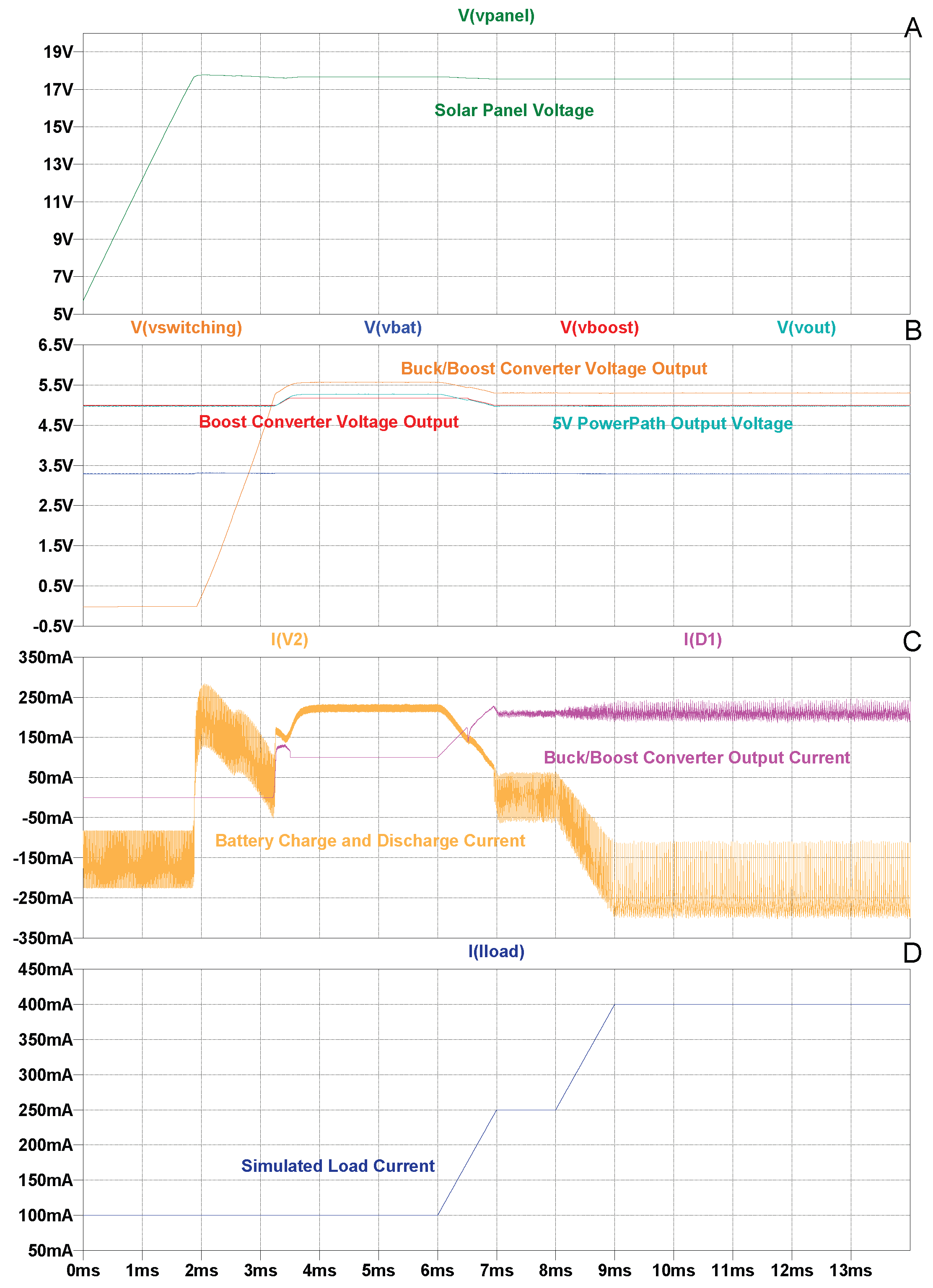
Figure 15 presents the transient response of the PowerPath circuit under partial-irradiance operation at G = 500 W / m 2 , representative of cloudy sky, early-morning, or late-afternoon conditions. Subplot A shows the solar panel voltage stabilizing at approximately 17.5 V after the initial startup ramp, confirming that the panel remains electrically active but with a limited power budget. During the low-load phase (up to approximately 7 ms ), the Buck/Boost main converter supplies the full load current while, simultaneously, the charger is delivering a small positive charging current to the battery, as evidenced by the mildly positive values of I ( V 2 ) in subplot C. As the simulated load current (subplot D) increases stepwise from 100 mA to 250 mA and subsequently to 400 mA , the solar-derived power budget is exceeded and the system undergoes a seamless source-sharing transition: the battery current reverses sign and ramps to approximately 250 mA averaged, indicating that the battery is now actively discharging to supplement the primary solar source and jointly sustain the load. Throughout this transition, the LTC4412 PowerPath controller continuously compares V SENSE against V IN and modulates the primary P-channel MOSFET accordingly, allowing both sources to contribute in proportion to their available energy rather than executing an abrupt all-or-nothing switchover. The critical result is visible in subplot B: the 5 V PowerPath output rail ( V o u t , cyan) remains flat and within specification across the entire load ramp, with no measurable undershoot, overshoot, or oscillation at the commutation point, validating the stability of the gate-drive control loop under source-sharing conditions. The Buck/Boost output current (subplot C, magenta) stays essentially constant at roughly 210 mA , confirming that the converter continues to deliver its maximum available current while the battery absorbs the deficit. This simulation validates the suitability of the PowerPath topology for IoT nodes subject to intermittent or degraded irradiance: rather than losing regulation when the primary source is insufficient, the system gracefully transitions to a cooperative dual-source mode, ensuring uninterrupted, well-regulated power delivery to the load without interruption or voltage perturbation.
  • Test 2—Peak irradiance and maximum load ( G = 1000 W / m 2 ).
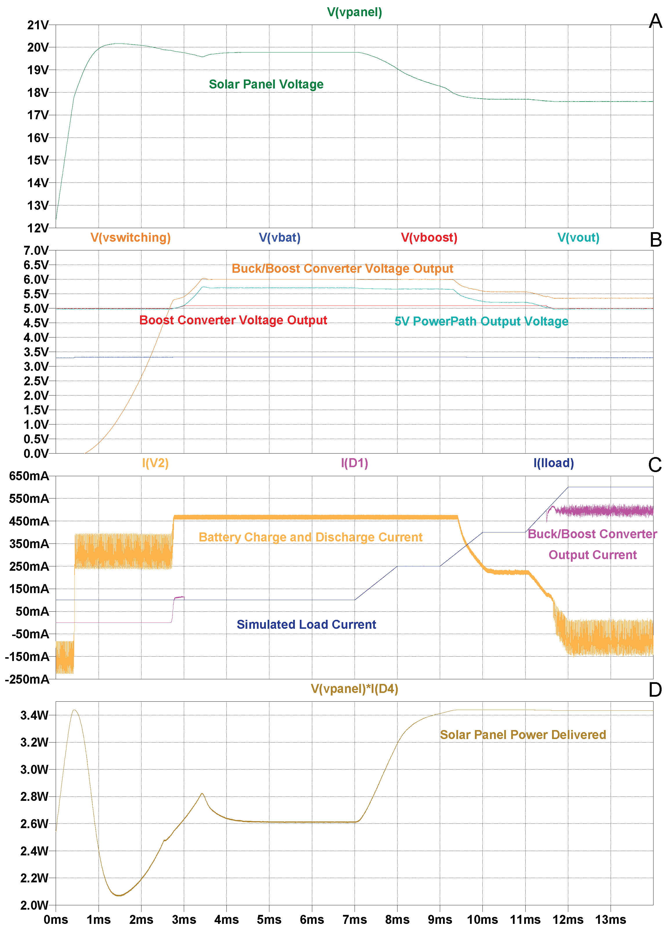
Figure 16 presents the steady-state and transient behavior under standard irradiance conditions ( G = 1000 W / m 2 ) with the system operating at maximum load. In this scenario, the Buck-Boost output dominates: the LTC4412 holds the primary MOSFET in full conduction and the backup path is reverse-biased by the body diode, drawing zero current from the storage element which loads at almost full power. The output rail exhibits excellent regulation, with voltage ripple well within acceptable limits. The conduction loss in the MOSFET is confined to P c o n d = I l o a d 2 · R D S ( o n ) , which is substantially lower than the equivalent Schottky dissipation, contributing to the overall system efficiency target. These results confirm that the PowerPath stage introduces no performance bottleneck under peak-power conditions.
It can be observed that only at the final stage of the test, when the load demand increases, the system begins to reduce the battery charging current to sustain the load current requirements. However, at a certain point, the Buck/Boost converter reaches its output current limit, requiring the discharge of the battery to supply the additional current demand.

2.5.3. Output Boost Regulation via LTC3525-5

The battery terminal voltage varies as a function of its state of charge (SoC), spanning a range that is incompatible with the fixed 5 V input level expected by the PowerPath stage. A dedicated boost regulation stage is, therefore, interposed between the battery output and the PowerPath input node, stepping the battery voltage up to 5 V so that it can serve as a valid and lossless alternative source alongside the solar-derived Buck/Boost output.
The LTC3525-5 Micropower Synchronous Boost Converter [28] was selected to provide this function. The device generates a fixed V O U T = 5 V output from an input range of 0.5 V to 4.5 V , which spans the entire discharge curve of the lithium-ion battery. Internal synchronous rectification eliminates the need for an external Schottky diode, and the converter achieves a peak conversion efficiency of up to η 95 % [28], a critical requirement for a solar-harvesting and battery-powered application where every milliwatt of avoidable dissipation reduces the energy available to the sensor payload.
A decisive factor in the selection of the LTC3525-5 for this design is its requirement for only three passive external components: one inductor and two ceramic capacitors. The reference design uses a 10 μ H shielded inductor together with a 10 μ F input capacitor and a 22 μ F output capacitor [28]. This minimal bill of materials reduces PCB area, assembly cost, and the potential for component-related failure modes—all of which are important considerations for a remote environmental sensor intended for long-duration unattended deployment.

2.5.4. Rail Stability Under Variable Input

By establishing a regulated 5 V input to the PowerPath stage, the LTC3525-5 ensures that the battery remains a viable power source throughout its discharge curve, from its fully charged terminal voltage down to the converter’s minimum operating threshold. Without this boost stage, a partially or deeply discharged battery would present a sub-threshold voltage to the LTC4412, preventing it from contributing to load support precisely when backup energy is most needed. The LTC3525-5, therefore, decouples the effective availability of the battery from its instantaneous SoC, guaranteeing that the PowerPath controller always sees two well-conditioned 5 V sources—the solar Buck/Boost output and the battery boost output—and can arbitrate between them transparently and without interruption to the downstream 5 V system bus. In conjunction with the lossless switchover provided by the LTC4412 stage, this architecture yields a robust, high-efficiency power delivery chain suited to the demanding constraints of autonomous solar-powered sensing systems.

2.6. Level Sensor Module

This section describes the design and implementation of a non-contact water level measurement module based on the Omron 2SMPP-02 piezoresistive MEMS gauge pressure sensor. The module combines a passive pneumatic measurement principle with an analog signal conditioning chain and is interfaced to the 12-bit successive-approximation ADC integrated within the ESP32 microcontroller.

2.6.1. Sensor Characteristics

The Omron 2SMPP-02 is a MEMS piezoresistive gauge pressure sensor. Its sensing element consists of a thin silicon diaphragm onto which four piezoresistors are arranged in a Wheatstone bridge configuration. When a differential pressure is applied, the diaphragm deflects, altering the resistance of each arm and producing a differential output voltage proportional to the applied pressure [29]. As a gauge-type device, the sensor measures pressure relative to local atmospheric pressure, which is the appropriate modality for the hydrostatic head measurement described in Section 2.6.2.
The rated measurement range is 0 to 37 kPa , with a typical full-scale span voltage of V span = 31 ± 3.1 mV at 37 kPa and 23   ° C . The device must be driven by a constant current source; the nominal drive current is I c c = 100 μ A . The bridge resistance is nominally 20 k Ω , and the typical offset voltage at zero differential pressure is 2.5 ± 4.0 mV .

2.6.2. Physical Measurement Principle

The measurement setup consists of a vertical PVC tube, approximately 2 m deep, buried vertically in the ground to serve as the measurement well. Rather than submerging the sensor at the bottom of the tube—which would require waterproofing and present maintenance challenges—a trapped-air capillary method is employed, allowing the sensor to remain at the surface in a protected location.
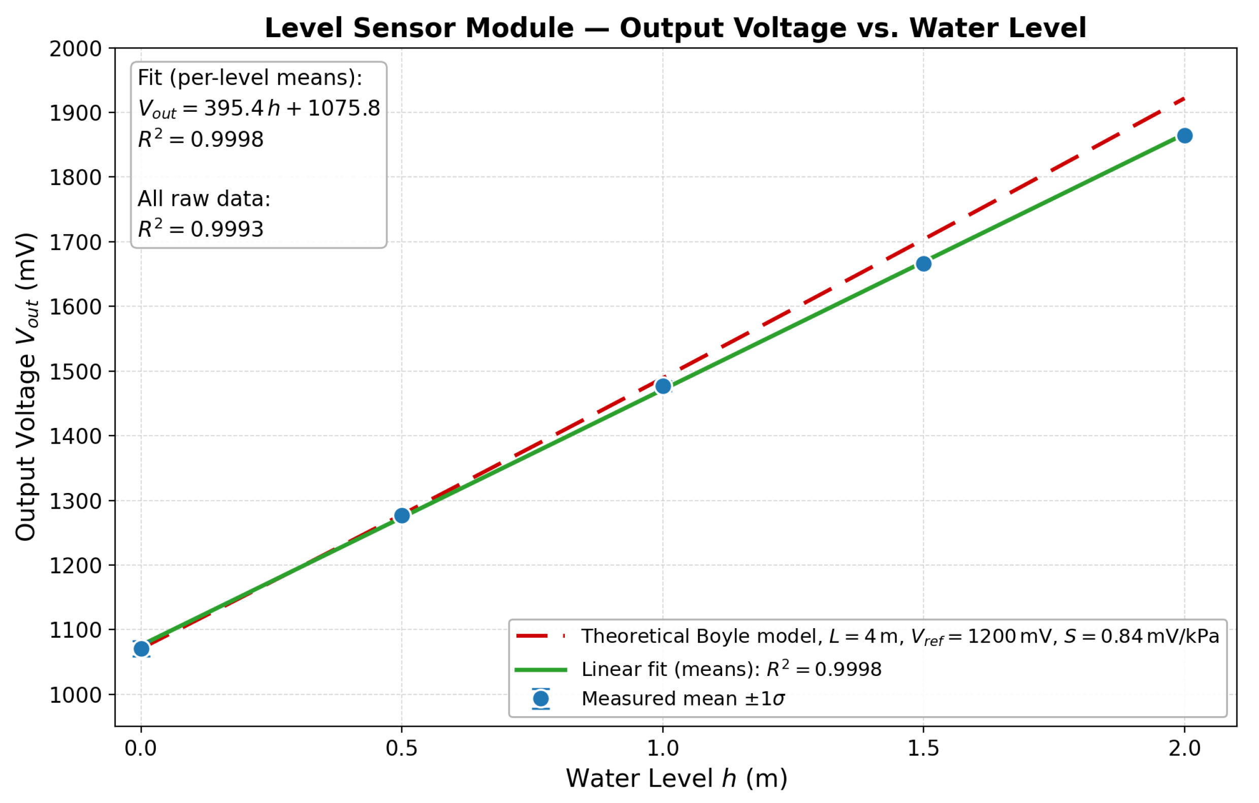
A thin capillary tube is routed from the 2SMPP-02 sensor’s pressure port downward to the bottom of the well. Initially, with the well empty, this capillary contains air at atmospheric pressure P 0 , and the sensor registers a gauge pressure of zero. As water rises inside the well to an external height h ext , it simultaneously enters the lower portion of the capillary and compresses the trapped air column. Because the water level inside the capillary ( h cap ) is generally lower than the external level—the air compression is only partial—the two heights are not equal and must be related through the combined hydrostatic equilibrium and the ideal-gas law (Boyle’s law at constant temperature).
At the air–water interface inside the capillary, the compressed air pressure must equal the net hydrostatic pressure at that point:
P air = P 0 + ρ g h ext h cap
where ρ 1000 kg / m 3 is the density of water and g 9.81 m / s 2 is the standard gravitational acceleration. Applying Boyle’s law to the sealed air column of initial length L (the capillary length):
P 0 · L = P air · ( L h cap )
Substituting Equation (9) into Equation (10) and expanding yields a quadratic equation in h cap :
ρ g · h cap 2 h cap P 0 + ρ g h ext + ρ g L + ρ g L h ext = 0
The physically meaningful root (positive and not exceeding h ext ) gives h cap , from which the gauge pressure measured by the sensor follows directly:
Δ P = P air P 0 = P 0 L L h cap P 0
This method isolates the sensor from direct contact with the water, significantly improving long-term reliability. The capillary tube diameter is chosen to be sufficiently small that surface tension and viscous effects are negligible at the quasi-static measurement rates employed in this application.

2.6.3. Hardware Design and Signal Conditioning

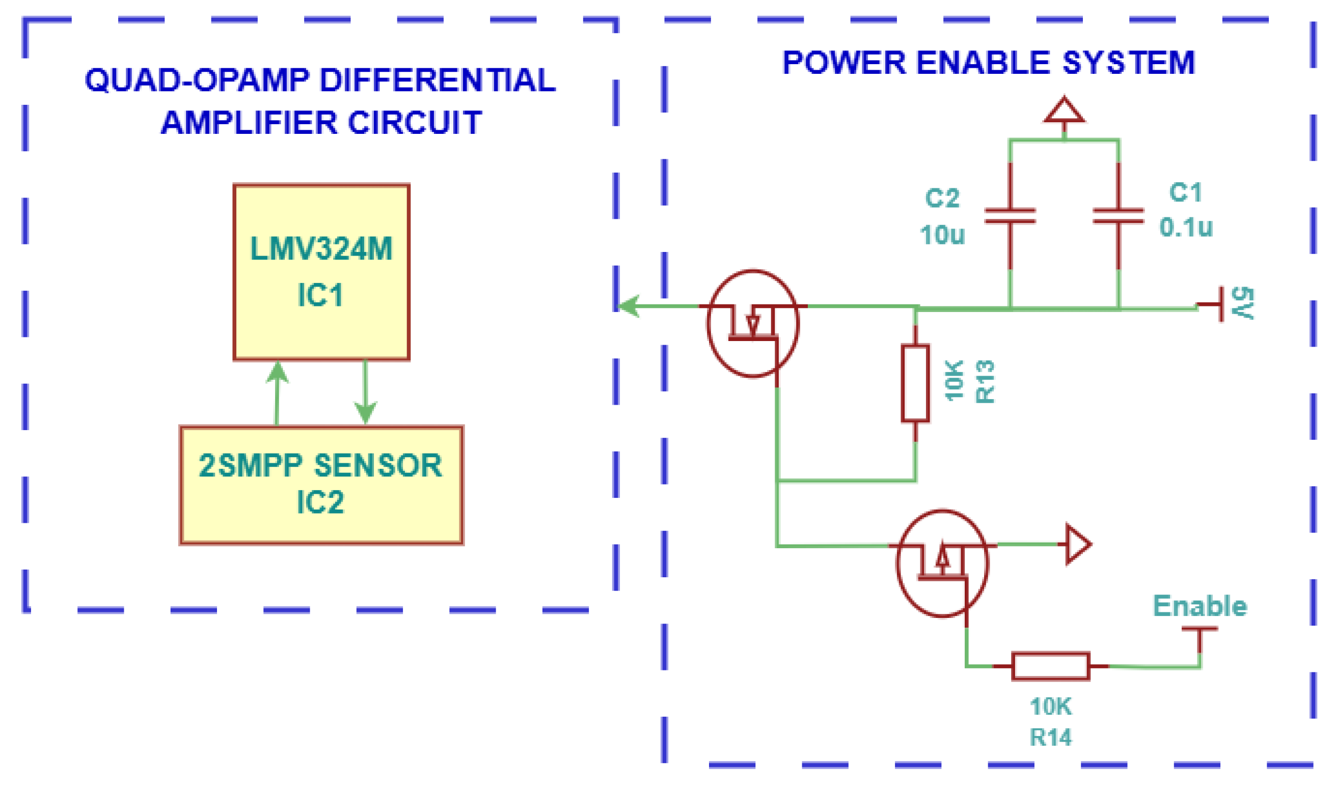
The raw differential output voltage of the 2SMPP-02 at full scale is only 31 mV , necessitating a dedicated signal conditioning chain to amplify the signal to a range suitable for the ADC. The implemented circuit, shown in Figure 17, is based on the manufacturer’s recommended reference topology which is represented in the “Figure 7. Example of Recommended Circuit Diagram for 2SMPP-02” of the reference [29], and consists of three functional blocks: a constant-current excitation circuit, a three-op-amp instrumentation amplifier, and a power management subsystem.

2.6.4. Constant-Current Excitation Circuit

The 2SMPP-02 must be driven by a stable 100 μ A constant current. Following the manufacturer’s recommended design [29], this is achieved with a Howland-type current source built around one amplifier of the LMV324 quad op-amp package, using a voltage divider formed by R 1 = 40 k Ω and R 2 = 10 k Ω referenced to V D D = 5 V , and a precision current-setting resistor R 3 = 10 k Ω . The resulting drive current is as follows:
I c c = V D D · R 2 ( R 1 + R 2 ) · R 3 = 5 V · 10 k Ω ( 40 k Ω + 10 k Ω ) · 10 k Ω = 100 μ A
A metal-film resistor with a low temperature coefficient is specified for R 3 to minimize gain drift over the operating temperature range.

2.6.5. Instrumentation Amplifier

The remaining three operational amplifiers of the LMV324 are configured as a standard three-op-amp instrumentation amplifier, as recommended in the manufacturer’s application note [29] and detailed in the LMV324 datasheet [30]. The LMV324 is a low-voltage (2.7 V to 5.5 V), rail-to-rail output, quad op-amp with a gain-bandwidth product of 1 MHz and a supply current of 410 μ A , making it well-suited for low-power, single-supply signal conditioning.
The first stage consists of two unity-gain-configured input buffers (using the resistor pairs R 4 = R 8 = 10 k Ω and R 5 = R 7 = 10 k Ω ) that present a high input impedance (>100 M Ω ) to the sensor bridge, preventing loading effects. The differential gain is set by the central resistor R 6 = 1 k Ω . The second stage is a unity-gain difference amplifier formed by R 9 = R 10 = 33 k Ω (the reference circuit suggest R 9 = R 10 = 10 k Ω but a 33 k Ω resistance value was chosen for this case to obtain gain value of almost 70) that performs the single-ended conversion and adds the reference offset voltage. The total instrumentation amplifier gain is given by the following:
G = 1 + 2 R 5 R 6 · R 9 R 4 = 1 + 2 × 10 k Ω 1 k Ω × 3.33 = 69.3
The output voltage of the instrumentation amplifier is, therefore
V o u t = G · ( V s + V o s ) + V r e f
where V s is the differential voltage produced by the sensor bridge, V o s is the offset voltage of the sensor and V r e f is the reference voltage applied to the lower rail of the output stage.

2.6.6. Reference Voltage Modification

A key design modification with respect to the manufacturer’s reference circuit is the substitution of the 1.0 V reference suggested in the datasheet with a 1.2 V reference generated by an LM385BZ-1.2 precision shunt voltage reference. This change shifts the quiescent ADC output voltage upward by 200 mV , providing additional headroom above ground to accommodate the sensor’s negative offset voltage (which can be as low as 6.5 mV at the extremes of the tolerance band), thereby ensuring that the amplified output signal does not saturate near the lower rail of the single-supply LMV324 under any operating condition. The LM385BZ-1.2 provides a stable 1.2 V reference with a low dynamic impedance and is bypassed by capacitor C 3 = 100 nF to suppress high-frequency noise.

2.6.7. Power Management Subsystem

To support low-power operation in field-deployed, battery-powered scenarios, the module incorporates a transistor-based power switching subsystem, shown in the POWER ENABLE SYSTEM block of Figure 17 (complete schematic is available in the supplementary files). The 5 V supply rail feeding the sensor and signal conditioning circuitry is controlled by a P-channel MOSFET (Q1) acting as a high-side switch, driven by an N-channel MOSFET (Q2) configured as a logic-level inverter.
A logic-high signal on the ENABLE line turns on Q2, which in turn pulls the gate of Q1 low, enabling the 5 V rail. Conversely, a logic-low on ENABLE turns off Q2, allowing the gate of Q1 to be pulled high via R 13 , thereby cutting power to the module. This arrangement allows the firmware to power the sensor module only during a measurement cycle—typically lasting a few hundred milliseconds—and keep it in a de-energized state otherwise, substantially reducing mean current consumption. Decoupling capacitors C 1 = 100 nF and C 2 = 10 μ F are placed at the switched 5 V rail to stabilize supply voltage transients during power-on.

2.6.8. Calculations and Expected Values

This subsection develops the complete signal chain from a physical water height h to the expected digital output code N of the ESP32 ADC, for the two boundary conditions of the measurement range.

2.6.9. Pressure Calculation

Applying the model described in Section 2.6.2, the gauge pressure at the sensor is obtained by solving Equation (11) for h cap and substituting into Equation (12). With ρ g = 9810 Pa / m , P 0 = 101,325 Pa , and capillary length L = 4 m , the quadratic becomes the following:
9810 h cap 2 h cap 101,325 + 9810 h ext + 39,240 + 39,240 h ext = 0
For the maximum well depth of h ext = 2 m , the physically valid root of Equation (16) is h cap = 0.506 m , giving the following:
Δ P max = P 0 L L h cap P 0 = 101,325 × 4 4 0.506 101,325 = 14.66 kPa
This value is well within the sensor’s rated range of 37 kPa , confirming that the sensor operates in its linear region over the full measurement range. Note that the simple hydrostatic estimate Δ P = ρ g h ext would predict 19.62 kPa , an overestimate of approximately 34 % relative to the Boyle-corrected value for L = 4 m , which is highly significant and underscores the importance of accounting for the actual capillary length in the model.

2.6.10. Sensor Raw Differential Voltage

The 2SMPP-02 exhibits a linear response over its rated range. The sensitivity S of the sensor is derived from its typical Span Voltage:
S = V span Δ P rated = 31 mV 37 kPa 0.84 mV kPa
The raw differential output voltage from the sensor bridge for a given pressure Δ P is , therefore
V s ( Δ P ) = S · Δ P = 0.84 mV kPa × Δ P
For the offset voltage ( V o s ), the typical value of 2.5 mV from the datasheet is assumed for nominal calculations. In a calibrated implementation, this offset is absorbed into the firmware’s linear calibration coefficients.

2.6.11. Amplifier Output Voltage

Substituting Equations (14), (18), and (12) into Equation (15), the amplifier output voltage as a function of water level is as follows:
V o u t ( h ext ) = G · [ S · Δ P ( h ext ) + V o s ] + V r e f
where Δ P ( h ext ) is the non-linear function defined by Equations (11) and (12). Because the Boyle-law correction introduces a mild non-linearity, V o u t is not strictly proportional to h ext ; a firmware look-up table or the analytical solution of the quadratic should be used for accurate height retrieval.
  • Case 1—Empty Tube ( h = 0 m ):
At zero water level, the applied pressure is Δ P = 0 kPa and the sensor bridge produces no differential signal ( V s + V o s = 2.5 mV ). The instrumentation amplifier output is determined solely by the reference and the sensor’s offset:
V o u t ( 0 ) = 69.3 × [ 2.5 mV ] + 1200 mV = 1026.75 mV
  • Case 2—Full Tube ( h ext = 2 m ):
From Equation (17), Δ P = 14.66 kPa . Applying Equation (19):
V s = 0.84 mV kPa × 14.66 kPa = 12.28 mV
The amplified output is then the following:
V o u t ( 2 ) = 69.3 × [ 12.28 mV 2.5 mV ] + 1200 mV
V o u t ( 2 ) = 677.75 mV + 1200 mV = 1877.75 mV
The voltage span is then the following:
V s p a n = V o u t ( 2 ) V o u t ( 0 ) = 1877.75 mV 1026.75 mV = 851 mV

2.6.12. ADC Mapping

The ESP32 microcontroller integrates a 12-bit successive-approximation ADC with a configurable input attenuation. In the ADC_ATTEN_DB_11 (11 dB) attenuation setting, the effective input voltage range is approximately 0 to 3.15 V , which encompasses both boundary values computed above. The ADC produces a digital output code N according to the following:
N = V o u t V r e f , A D C × ( 2 n 1 )
where n = 12 is the ADC resolution (giving 2 12 = 4096 quantization levels) and V r e f , A D C = 3.15 V is the ADC full-scale reference voltage.
  • Case 1—Empty Tube ( V o u t = 1026.75 mV ):
N e m p t y = 1026.75 3150 × 4095 0.326 × 4095 = 1335 counts
  • Case 2—Full Tube ( V o u t = 1877.75 mV ):
N f u l l = 1877.75 3150 × 4095 0.596 × 4095 = 2440 counts
The expected dynamic range of the ADC output over the full 0– 2 m measurement span is, therefore, Δ N = 2440 1335 = 1105 counts . Given a 12-bit ADC with a full-scale range of 4096 counts, this represents a utilization of approximately 26.98 % of the ADC’s dynamic range. The theoretical height resolution of the system is as follows:
δ h = 2 m 1105 counts 1.81 mm count
Table 1 summarizes the complete signal chain values at the boundary conditions.

3. Build Instructions

This section provides a complete, step-by-step guide for replicating the prototype, covering PCB fabrication and assembly, enclosure preparation, internal wiring, and field installation of the measurement well. All design files required to reproduce this work—including KiCad schematics, PCB layouts, gerber manufacturing packages, and firmware—are provided as Supplementary Materials.

3.1. Materials and Tools

The following equipment is required for the assembly of the prototype. Standard soldering tools and basic electronic test instruments are sufficient. Electronic tools:
  • Temperature-controlled soldering station (recommended: 330– 360   ° C tip temperature).
  • Digital multimeter.
  • Fine-tipped tweezers and SMD solder paste (63/37 Sn/Pb or lead-free SAC305).
  • Flux pen and isopropyl alcohol (≥99%) for board cleaning.
  • Oscilloscope (optional, but recommended for power-rail verification).
  • Mechanical tools:
  • Hand drill or drill press with 6 mm and 10 mm HSS bits.
  • PVC pipe cutter or hand saw.
  • Manual or motorized earth auger capable of drilling a 100 mm borehole to a depth of 2 m .
  • Utility knife and cable ties.
  • Silicone sealant (weatherproof, UV-stable) and waterproof cable glands (PG7 or equivalent).
The complete Bill of Materials for the two PCBs is listed in Table 2. All KiCad project files and gerber packages are provided in Supplementary Materials S1–S4 (see the Supplementary Materials Table).

3.2. Step 1 — Electronic Assembly (PCB Fabrication and Soldering)

3.2.1. PCB Fabrication

  • Export the gerber files from the KiCad projects provided in Supplementary Materials S3 and S4. The manufacturing specification targets a two-layer FR4 board, 1.6 mm thick, with HASL or ENIG surface finish, and a minimum trace width and clearance of 0.2 mm .
  • Submit the gerber packages to a PCB manufacturer (e.g., JLCPCB or PCBWay).

3.2.2. Component Soldering

  • Arrange components in the order listed in Table 2. Place the smallest passive components (0402 resistors and capacitors) first, followed by ICs, inductors, and through-hole components like connectors last.
  • Apply solder paste to SMD pads using a stainless-steel stencil (0.12 mm thickness) or a fine-tipped syringe.
  • Place all SMD components using fine-tipped tweezers, aligning pin 1 markers with the silkscreen. For the LTC3130 (QFN-20) and LT3652 (DFN-12), ensure the exposed thermal pad is centred over its PCB footprint.
  • Reflow the board in a controlled-temperature oven or on a hotplate. Follow the recommended solder paste profile: preheat to 150   ° C , ramp to 245   ° C peak (SAC305), then cool at ≤4 ° C s 1 .
  • Hand-solder all through-hole components (2SMPP-02 sensor, connectors, and the LM385BZ-1.2 voltage reference) on the sensor module board.
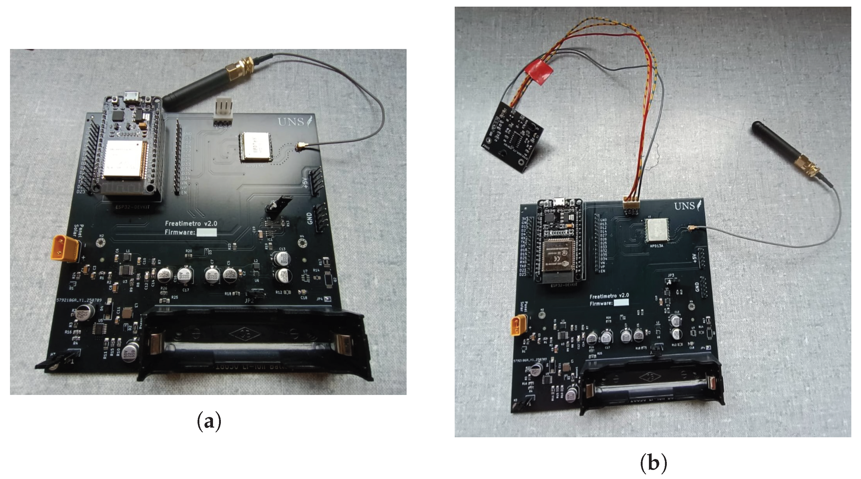
  • Clean both boards with isopropyl alcohol (≥99%) and a soft brush to remove flux residue. Allow to dry completely before testing. Final assembled PCBs can be observed in Figure 18.

3.2.3. Electrical Verification

  • Using a multimeter in continuity mode, check all GND and power net connections against the schematic. Verify that no shorts exist between VCC and GND rails.
  • Apply 5 V DC to the system input via a bench power supply with a current limit set to 100 mA . Confirm that the quiescent current draw does not exceed the expected idle consumption of the design.
  • Measure the regulated output of the LTC3130 stage with a multimeter. Verify that it falls within the programmed output voltage ± 5 % .
  • Confirm continuity on the 4-pin inter-board connector signals: GND, +5 V, ENABLE, and OUT_SGN.
  • Flash the ESP32 firmware (Supplementary Material S6). Confirm successful compilation and device boot via the serial console.

3.3. Step 2—Enclosure Preparation

The system electronics must withstand outdoor exposure at the wellhead, including precipitation, UV radiation, and dust. An IP67-rated ABS or polycarbonate enclosure with minimum internal dimensions of 100 × 68 × 50 mm is recommended.
  • Select a waterproof enclosure with a neoprene or silicone gasket and a minimum ingress protection rating of IP67 per IEC 60529.
  • Drill two entry ports on the bottom face of the enclosure: a 6 mm hole for the PTFE capillary tube (PG7 cable gland) and a 10 mm hole for the solar panel cable (PG9 cable gland).
  • Secure the main board and the sensor module PCB to the enclosure floor using M2 brass standoffs ( 10 mm height) and M2 screws.
  • Pass the PTFE capillary tube through its cable gland, leaving a service loop of ≈30 mm inside the enclosure before connecting to the 2SMPP-02 pressure port. Tighten the cable gland to form a gas-tight seal.

3.4. Step 3—Internal Connections

  • Connect the sensor module PCB to the main board using the 4-pin cable, carrying GND, +5 V, ENABLE, and OUT_SGN signals. Verify polarity before applying power.
  • Solder the connector for the solar panel and connect it to the board. Verify the positive ( V + ) and negative ( V ) wires of the solar panel are properly connected to the positive and negative of the board.
  • Place the single-cell Li-Ion battery in the battery holder on the main board, observing polarity (BAT+/BAT−).
  • Apply power via the solar panel input (or a bench supply at V I N = 17.5 V ). Verify that
    • The LTC3130 output rail is correctly regulated.
    • The 5 V rail measures 5.0 V ± 5 % .
    • The ESP32 boots successfully and the ENABLE pulse activates the sensor module power rail.
  • Dress all internal wiring with cable ties to prevent contact with sharp PCB edges or the enclosure lid gasket. Ensure the lid can close freely and the gasket seats uniformly before field installation.

3.5. Step 4—Field and Sensor Installation

3.5.1. Well Preparation

  • Select a representative measurement site, avoiding locations subject to surface runoff contamination or mechanical disturbance.
  • Using a motorized or manual earth auger ( 100 mm ), drill a vertical borehole to a depth of 2 m . Remove all loose spoil from the borehole and verify the walls are stable.

3.5.2. Well Casing Construction and Pre-Installation

  • Cut a section of Schedule 40 PVC pipe (⌀ 75 mm) to a total length of 2.5 m (providing 0.5 m of surface protrusion for coupling to the enclosure).
  • Using a hand drill with a 3 mm bit, perforate the lower 1.8 m of the pipe with rows of slots spaced 20 mm apart, each slot being 1– 2 mm wide. These perforations allow groundwater ingress while the slot width prevents coarse sediment entry.
  • Wrap the perforated section of the pipe tightly in a single layer of non-woven geotextile filter mesh (≤0.5 mm apparent opening size). Secure the mesh at both ends with stainless-steel cable ties to prevent slippage during insertion (Optional).
  • Critical step: Before inserting the pipe into the borehole, route the PTFE capillary tube from the top of the pipe to the bottom along the interior pipe wall. Adhere the tube to the inner wall at 300 mm intervals using waterproof silicone sealant or cable clips, ensuring the tube exit is flush with the bottom of the pipe. This step is essential to prevent the capillary tube from coiling or shifting after installation, which would compromise the pneumatic measurement column.
  • Allow the silicone adhesive to cure for a minimum of 2 h before proceeding.
  • Do not forget to put the bottom lid of the PVC tube to close it.

3.5.3. Final Assembly and Sealing

  • Lower the cased pipe assembly vertically into the borehole until 0.5 m of pipe protrudes above ground level. Backfill any annular gap between the pipe and borehole wall with clean gravel (5– 10 mm aggregate) in the lower 1.5 m , and with compacted native soil in the upper 0.5 m to form a surface seal.
  • Feed the capillary tube up through the top of the pipe and trim it to a length that reaches the pressure port of the 2SMPP-02 sensor inside the enclosure with a 30 mm service loop.
  • Place the waterproof enclosure over the protruding pipe top so that it acts as a sealed weatherproof cap. Align the bottom cable gland with the pipe interior and secure the enclosure to the pipe using a jubilee clip or a custom-machined PVC adapter. Apply a bead of silicone sealant around the pipe-to-enclosure interface to prevent ingress of surface water.
  • Connect the free end of the PTFE capillary tube to the pressure port of the 2SMPP-02 sensor. The recommended tube inside diameter is 2 mm as specified in the sensor datasheet [29]. Ensure the connection is airtight; any leak in the pneumatic column will produce a systematic underestimation of measured water height.
  • Orient and mount the solar panel on a south-facing bracket at a tilt angle equal to the local site latitude. Route the solar cable down to the enclosure cable gland and tighten.
  • Close and latch the enclosure lid. Confirm that the gasket is correctly seated and that all cable glands are tightened to their rated torque.

4. Operating Instructions

Once the device has been fully assembled and installed, the operator must carry out the following commissioning procedure to bring the node into service.
  • Pre-installation calibration. Prior to field installation, a two-point calibration of the level sensor module must be performed using the procedure described in Section 4.1.
  • Physical installation. Mount the enclosure on the casing pipe and connect all external cables: the solar panel lead, the sensor capillary tube, and the LoRa antenna. Verify that all cable glands are tight and the enclosure lid is properly latched.
  • Battery connection. Insert the lithium-ion battery pack and connect it to the battery slot on the main board. Ensure the cell is adequately pre-charged before deployment to guarantee operation during the first night cycle.
  • System reset. With the battery connected and the solar panel exposed to ambient light, force a hard reset by pressing the EN button on the ESP32 module. The node will boot, initialize the LoRa transceiver, and begin transmitting periodic measurement packets.
  • Link verification. At the master node location, confirm that data packets from the newly installed sensor node are being received and correctly relayed to the cloud back-end. Signal quality indicators (RSSI and SNR) should be inspected to ensure a reliable radio link.
Once these steps have been completed and a valid link has been confirmed, the node operates autonomously without further intervention.

4.1. Two-Point Calibration

The pressure sensor is calibrated using a two-point procedure accessible via Bluetooth Classic SPP. Calibration data is stored in non-volatile memory (NVS) and persists across power losses and deep-sleep cycles; consequently, the procedure need only be repeated if the physical installation geometry changes or the operator explicitly wishes to recalibrate the unit.

4.1.1. Entering Calibration Mode

Calibration mode is entered through a deliberate two-step hardware sequence designed to prevent accidental activation during normal operation:
  • Press the EN button on the ESP32 module to trigger a hard reset.
  • Within 5 s of the reset, press and hold the RESET_CAL button for 10 s.
Once this sequence is completed successfully, the node enters calibration mode and becomes Bluetooth-discoverable for 60 s under the device name Freatimetro. The operator connects from any device using a standard serial terminal application over the Bluetooth SPP profile and is presented with a command-line interface.

4.1.2. Calibration Procedure

The calibration requires two physical reference conditions and a geometric parameter:
  • Zero point—With the capillary tube empty and open to atmosphere ( h = 0 ), the operator issues the zero command. The firmware reads the ADC output voltage and stores it as V 0 .
  • Full-scale point—With the tube filled to a known reference depth h cal (configured via set h <cm>), the operator issues the full command to record the corresponding ADC voltage V full .
The physical capillary tube length L is set with set L <m> to match the installed geometry. Alternatively, both reference voltages can be entered manually via set zero <mV> and set full <mV> when direct ADC access is not practical (e.g., bench calibration using known reference values).
Once both reference points are available, the calibrate command computes the effective offset V 0 , eff and sensitivity K eff [ mV kPa 1 ] using the sealed-tube pressure model (Boyle’s law, solved analytically as a quadratic), and saves the result to NVS. The operator finalizes the session with the exit command, which permanently disables the Bluetooth stack to free heap memory for normal operation.

4.1.3. Persistence and Recalibration

The calibration coefficients stored in NVS survive all power interruptions and deep-sleep cycles and are automatically loaded on every subsequent boot. Because the data are written to non-volatile storage, the only way to clear or update a calibration is to repeat the hardware entry sequence described above. Operators should, therefore, label each unit with its calibration date and reference conditions for traceability.

4.2. Software Operation

The firmware of both node types—master transceiver and sensor node—is implemented on the ESP32 microcontroller using FreeRTOS, a real-time operating system. This architecture decomposes each device’s behavior into independent concurrent tasks, allowing time-critical operations, like radio protocol handling, to run at high priority without being blocked by lower-priority activities such as cloud communication.

4.2.1. Master Node

The master transceiver firmware is structured around four FreeRTOS tasks distributed across the two processor cores of the dual-core ESP32, as illustrated in Figure 19.
Core 1 hosts the two radio-related tasks. The highest-priority LoRa task is exclusively responsible for time-critical radio operations: it parses incoming packets, transmits response frames, and drives the communication state machine. To guarantee that no LoRa preamble is missed, this task avoids all slow I/O—it only reads the radio FIFO and enqueues records for downstream processing. A secondary Sensors task, running at medium priority on the same core, reads the battery voltage via the ADC and samples the charger status pins at a configurable reporting interval. A two-second guard period prevents the Sensors task from issuing a report while a LoRa exchange is in progress.
Core 0 hosts the two connectivity tasks. The Wi-Fi task manages network association with exponential back-off reconnection, NTP time synchronization, OTA firmware updates over-the-air, mDNS service advertisement, and the Telnet remote console. The lowest-priority Firebase task drains the inter-task queue every 15 s, pushing LoRa and charger records to the Firebase Realtime Database.
Inter-task communication relies on a 500-slot FreeRTOS queue fed by both Core 1 tasks and consumed by the Firebase task, a console mutex that prevents interleaved Serial and Telnet output, and a set of atomic flags for Wi-Fi and Firebase readiness signals.

4.2.2. Sensor Node

The sensor node firmware follows the same FreeRTOS task-based architecture and also runs on an ESP32, but is additionally optimized for minimal energy consumption to maximize battery and solar operating life.
Three coordinated tasks handle the node’s operation:
  • The measurement task acquires a reading from the level sensor module at each scheduled sampling instant and packages it into a LoRa payload.
  • The communication task transmits the payload to the master node and awaits acknowledgement, implementing the necessary request–response handshake.
  • The sleep and synchronization task governs the node’s power state. Between measurement cycles, the ESP32 enters deep-sleep, with a hardware timer configured to wake the processor at the next scheduled sampling time.
A dedicated LoRa interrupt line (connected to the SX1276 DIO0 pin) can wake the node at any time to handle an incoming command or configuration update from the master, even when the processor is in its low-power sleep state. This mechanism allows the master node to reach any sensor node on demand without waiting for the next scheduled wake-up.
Together, the sleep timer and the LoRa interrupt allow the sensor node to spend the vast majority of its time in deep-sleep, drawing only microamp-level standby current, while remaining fully responsive to both periodic measurement schedules and asynchronous network events.

5. Validation with Experimental Testing

5.1. Power and Charger System

A multi-day field trial was conducted to validate the operation of the solar energy harvesting and battery charging subsystems under realistic outdoor conditions. The primary objective was to verify the correct alternation of the whole system charging cycle, power supply and to obtain a first characterization of the system’s energy consumption under the current firmware configuration, which has not yet been optimized for minimum power draw.

5.1.1. Test Setup and Methodology

The sensor node was deployed outdoors in Bahía Blanca, Argentina, with the solar panel exposed to natural sunlight. The firmware was configured to transmit one LoRa packet every 15 min; each packet included the battery voltage, the LT3652 charger state, and the LoRa link-quality metrics (RSSI and SNR). All received packets were stored in a Firebase real-time database via the gateway node. The trial ran continuously from 17 May 2026 at 13:21 to 22 May 2026 at 06:47 (UTC−3), spanning a total of 4 days, 17 h, and 26 min.
The battery voltage V B A T is measured by the ESP32’s 12-bit ADC through a resistive voltage divider ( R 1 = 1.212 M Ω , R 2 = 650 k Ω ) and converted to millivolts according to the following:
V B A T = V A D C · R 1 + R 2 R 2 · k c = V A D C · 2.865 · 0.955
where V A D C is the voltage at the ADC input pin (derived from the 12-bit ADC reading and a 3.15 V internal reference) and k c = 0.955 is an empirically determined correction factor. The single-cell Li-Ion battery used in this trial has a nominal capacity of 3000 mAh, with a maximum float voltage of 4.1 V and a lower cutoff voltage of approximately 3.0 V.
It is important to emphasize that in this test configuration the SX1276 LoRa transceiver remained continuously in standby mode, drawing a measured current of approximately 7–8 mA. Furthermore, the 15-min sampling interval was selected solely to obtain a dense time-series of the battery state during this validation trial; the final application requires only four or fewer transmissions per day, which is sufficient for groundwater monitoring purposes. Both factors imply that the energy consumption characterized here represents a worst-case scenario, with substantial headroom for power optimization (see Section 5.1.4).

5.1.2. Meteorological Conditions During the Trial

Table 3 summarizes the sky and precipitation conditions for each day of the trial, as reported by Argentina’s National Meteorological Service (SMN). The five-day period presented variable conditions, with predominantly clear days on 17–18 May followed by increased cloud cover and a rain event on 20 May. These conditions are directly reflected in the battery voltage time series discussed below.

5.1.3. Observed Charge–Discharge Behavior

Figure 20 presents the complete time series of V B A T (blue line, left axis) and the LT3652 charger state (dashed red line, right axis) over the duration of the trial.
Five complete charge–discharge cycles are clearly identifiable, each corresponding to one solar day. During daylight hours, the LT3652 drives a CC/CV charge cycle, raising V B A T toward the programmed float voltage of 4.1 V. Once the charge current falls below the C/10 termination threshold ( I C H G < 50 mA , corresponding to one tenth of the 500 mA maximum charge current), the charger enters Standby/Full mode and V B A T stabilizes near its open-circuit value. At night, with no solar input available, the battery supplies the node’s standby load, producing a gradual, monotonic voltage decrease until the following sunrise restarts the charging cycle. No fault state and no deep-discharge event were recorded at any point during the trial, confirming that the system maintains energy autonomy under the tested conditions.
The charger state transitions confirm correct LT3652 operation throughout the trial. On the most demanding cycle (18 May), the battery reached a minimum of 3.821 V after approximately 14.4 h of overnight discharge from a starting voltage of 4.016 V. The LT3652 re-engaged charging when solar irradiance became available in the morning, successfully restoring V B A T to 4.128 V within the available daylight window. Once the CC/CV cycle completed and the current fell below C/10, the charger entered Standby/Full and the brief Charging pulses visible in Figure 20 correspond to the auto-recharge event triggered when V B A T drops 2.5% below the float setpoint ( V B A T 4.0 V ), which is the normal operating mode specified in the LT3652 datasheet. This behavior is consistent with the simulation results presented in Section 2.4.
The reduced charging peak on 20 May, in which V p e a k reached only 4.057 V compared with 4.128 V on clear days, is consistent with the overcast and showery conditions recorded by the SMN for that day, which reduced the available solar irradiance and consequently limited the energy delivered by the panel.

5.1.4. Preliminary Power Consumption Estimate

Based on the independently measured current draw—approximately 7–8 mA from the SX1276 LoRa module in standby mode plus less than 10 μ A from the ESP32 in deep sleep—the total average system consumption under the current (non-optimized) firmware is estimated at I ¯ c u r r e n t 7.5 mA . Applying this value to the two most representative overnight discharge intervals yields the consumed charge estimates shown in Table 4.
Even under the worst-case Night 3 interval—which extended over 22.8 h due to the overcast conditions of 20 May limiting daytime charging—the estimated consumed charge of 171 mAh represents only 5.7% of the battery’s 3000 mAh capacity. This result confirms that, at the current consumption level, the battery is far from being fully depleted overnight and the system maintains a comfortable energy margin even on days with reduced solar irradiance.
These figures also define a clear starting point for power optimization. In the final application, a possible solution is that the LoRa transceiver and the ESP32 will be powered down between measurement events using hardware power-gating, so that each wake-cycle consists only of a brief active window of a few seconds followed by deep sleep. With four transmissions per day and a typical active-window current of approximately 80 mA for ∼5 s per cycle, the average quiescent current reduces to the following:
I ¯ o p t = I a c t i v e · t a c t i v e + I s l e e p · ( T c y c l e t a c t i v e ) T c y c l e
I ¯ o p t = 80 mA × 5 s + 0.01 mA × 21,595 s 21,600 s 0.0285 mA
representing a reduction of approximately two orders of magnitude with respect to the current configuration. Under such a duty cycle, the daily energy budget would be entirely covered by even a small fraction of the available solar harvest, enabling indefinite autonomous operation with a wide margin to accommodate cloudy days or seasonal variations in solar irradiance.

5.2. Level Measuring Module

The level measurement module was characterized by filling a 3 m PVC tube (water column up to 2 m ) in incremental steps of 0.5 m while recording the digitized output voltage. The complete dataset consists of 69 readings distributed across five reference levels ( h = 0 , 0.5 , 1.0 , 1.5 , 2.0 m ), covering both the ascending and descending strokes.

5.2.1. Measured Signal Values

Table 5 summarizes the per-level statistics of the output voltage V o u t obtained from the ADC readings (already expressed in mV). The number of samples was N = 15 for all five levels and includes both the ascending and descending passages.
The standard deviation is below 8 mV at all levels, and below 4 mV for h 0.5 m . The slightly larger dispersion at h = 0 m ( σ = 12.16 mV ) is consistent with the pneumatic settling transient of the trapped-air capillary immediately after the tube is emptied.

5.2.2. Linearity Analysis

A least-squares linear regression was applied to the five per-level means to characterize the linearity of the V o u t h relationship. Using the model V ^ o u t = m · h + b , the fitted parameters and goodness-of-fit metric are as follows:
V ^ o u t ( h ) = 395.4 · h + 1075.8 [ mV ]
R 2 = i ( V ^ i V ¯ ) 2 i ( V i V ¯ ) 2 = 0.9998
Repeating the regression on all 69 raw ADC readings (to confirm that sample-to-sample dispersion does not degrade linearity) yields R 2 = 0.9993 . Both values exceed 0.999 , confirming that the V o u t h relationship is highly linear over the full 0– 2 m range. Figure 21 shows the measured means with ± 1 σ error bars, the linear fit, and the theoretical curve derived from the nominal signal chain parameters (INA gain G = 69.3 , sensor sensitivity S = 0.84 mV / kPa , and generic reference voltage value V r e f = 1200 mV ).
Figure 22 complements the linearity plot by showing all individual raw readings alongside the per-level mean ± 1 σ bands, making the repeatability of the system across both measurement strokes visible.

5.2.3. Comparison with Theoretical Values

To properly assess the agreement between the model and the measurements, two sets of theoretical predictions are considered: the nominal model, which uses the design parameters ( L = 4 m , I c c = 100 μ A , V r e f = 1200 mV , V o s = 2.5 mV ) and the adjusted model, which substitutes the actual experimental conditions measured during the characterization test ( L = 4 m , I c c = 95 μ A , V r e f = 1237 mV , V o s = 2.40 mV ). The reduced excitation current results from V D D = 4.75 V instead of the nominal 5.0 V while the reference voltage value V r e f = 1237 mV is obtained from its measurement.
The adjusted model predictions are computed as follows. The quiescent output at h = 0 is as follows:
V o u t ( 0 ) = G · V o s + V r e f = 69.3 × ( 2.40 mV ) + 1237 mV = 1070.7 mV
and at h = 2 m , with Δ P max = 14.66 kPa (Equation (17)) and S adj = 0.838 × ( 95 / 100 ) = 0.796 mV / kPa :
V o u t ( 2 ) = G · ( S adj · Δ P max + V o s ) + V r e f
V o u t ( 2 ) = 69.3 × ( 0.796 × 14.66 2.40 ) + 1237 = 1879.3 mV
The adjusted span is, therefore, the following:
Δ V o u t , adj = V o u t ( 2 ) V o u t ( 0 ) = 1879.3 1070.7 = 808.6 mV
Table 6 summarizes the comparison across both models.
The measured height resolution of the system results in the following:
N r e s = 794.15 3150 × 4095 0.252 × 4095 = 1032 counts
R E S m e a s u r e d = 2 m 1032 counts = 1.94 mm count
The adjusted model shows excellent agreement with the measurements across all parameters. The quiescent output is reproduced virtually exactly, while the span presents a relative error of 1.82 % , which is an acceptable value and thus a calibration is recommended before installing the device. This residual discrepancy is consistent with the possibility of cumulative effects of resistor tolerances on the actual INA gain or PCB design effects on the impedance that can affect the amplifier’s gains. No anomalous behaviors are present; the sensor and signal chain are operating within their rated specifications.

5.3. Communication Tests

The radio link range between the sensor node and the master gateway was characterized through a field test. The master node was installed on the rooftop of the Electrical and Computer Engineering Department (UNS, Bahía Blanca, Argentina) at coordinates: 38 . 6948 S, 62 . 2485 W on a metallic antenna mast, adding approximately 10 m above the GPS-measured ground level. The mobile node was carried by an operator along a route covering distances from 0 to 8.51 km from the master. Both nodes operated with identical LoRa physical layer parameters: spreading factor SF7, bandwidth 125 kHz, and coding rate 4/5. Transmit power was set to 15 dBm on the mobile node and 20 dBm on the master node.
During the test, the mobile node transmitted ping packets continuously while the master replied with pong packets. Radio events were recorded simultaneously through two independent sources: a Bluetooth serial log on the mobile device, capturing RSSI, SNR, and RTT for each exchange, and a GPS track with annotated waypoints, where the operator manually recorded the signal parameters at each measurement stop. The two logs were synchronized by detecting the natural activity gaps in the Bluetooth serial log: between consecutive waypoints, the operator moved without transmitting, producing silent intervals that define non-overlapping temporal windows for each measurement point. This allowed cross-validation of the manually annotated values against the automatically recorded log, confirming the consistency of both data sources. RSSI (Figure 23), SNR (Figure 24), and RTT statistics reported here are computed from the Bluetooth serial log over the corresponding window for each waypoint. The measured RTT remained essentially constant at approximately 113 ms across all distances, composed of the combined time-on-air of the ping and pong packets (≈26 ms each) plus the firmware processing delays defined by code at both the mobile and master nodes; propagation time is negligible at the distances tested (below 30 μ s at 8.51 km) and does not contribute to the RTT budget.

Measurement Results

Table 7 summarizes the per-waypoint results ordered by increasing distance from the master node. The elevation profile of the test route obtained from the GPS data can be visualized in the Figure 25.

6. Results and Discussion

The complete system was validated through LTSpice circuit simulations and field tests, with all subsystems performing within or above their design targets. Power management. The LTC3130 Buck-Boost converter maintained a regulated 5 V output across the full irradiance range of the panel (200– 1000 W / m 2 ), with a simulated steady-state efficiency of 85– 90 % . The LT3652 solar charger achieved an average conversion efficiency of 84.1 % at a charge current of 400 mA (and almost 90 % at lower charge current rates), with correct CC/CV operation, clean C/10 termination, and auto-recharge cycling confirmed by both simulation and the field trial, with behavior fully consistent with the circuit model of Section 2.4. The LTC4412 PowerPath controller executed source commutation without measurable output voltage perturbation under all simulated load profiles (100– 600 mA ), as demonstrated in Figure 15 and Figure 16. One identified hardware limitation is the LTC3525-5 boost converter, whose maximum output current of 175 mA at V O U T = 5 V [28] is adequate for the current load but may become a bottleneck if the sensor payload is expanded or the transmitter is set at maximum power. Replacement with a higher-current device (e.g., LTC3428, TPS61023 or similar) is recommended for future revisions. All other power-stage results were consistent with the design calculations and simulations.
Energy autonomy. The five-day field trial confirmed autonomous operation across multiple day–night cycles, including showery days, without any deep-discharge event. The average standby consumption of the current non-optimized firmware is I ¯ 7.5 mA , dominated by the SX1276 LoRa module operating in continuous standby. Taking the battery’s nominal capacity of 3000 mAh and assuming, as a worst-case bound, complete absence of solar charging (e.g., prolonged overcast conditions or nighttime-only operation), the non-optimized firmware could sustain the system for approximately 3000 mAh / 7.5 mA 400 h , or nearly 17 days, before reaching full discharge. This already exceeds the duration of any realistic sunless period at the target deployment latitude, and is consistent with the field-trial results, where the worst single overnight interval (Night 3, under overcast skies) consumed only 171 mAh out of the 3000 mAh capacity (5.7%) despite lasting 22.8 h, and was still fully replenished by the following day’s charging cycle. The 15-min sampling interval used during the trial was selected solely to obtain a dense time-series for validation purposes; the final deployment will require no more than four transmissions per day. With duty-cycled power gating—powering both the ESP32 and the LoRa module only during a brief active window—the estimated average consumption drops to I ¯ o p t 0.028 mA (Equations (31) and (32)), a reduction of approximately two orders of magnitude. Under this optimized profile, the same worst-case, zero-solar-input estimate yields an autonomy on the order of 3000 mAh / 0.028 mA 4460 days (over 12 years) without recharging, a figure that is in practice bounded by the Li-Ion cell’s shelf-life and self-discharge rather than by the system’s own power draw, and confirms that even repeated multi-day periods of low or absent irradiance pose no risk of depleting the battery. This can be achieved by setting the ESP32 into deep-sleep mode, the LoRa module into sleep mode and adopting a scheduled communication window strategy where master and slave nodes synchronize their active periods in time.
Level sensor. The level measurement module demonstrated excellent linearity ( R 2 = 0.9998 ) over the full 0– 2 m measurement range, with a span relative error of only 1.82 % with respect to the adjusted theoretical model—a residual attributable to cumulative resistor tolerances. The real height resolution measured was ≈1.94 mm / count . A two-point calibration is recommended prior to field installation to compensate.
LoRa communication. Table 7 summarizes the results of a field test conducted across ten waypoints at increasing distances from the base station, using a conservative configuration of SF7, 125 kHz bandwidth, and a transmit power of only 15 dBm on the mobile node. A radio link of up to 8.51 km was demonstrated in an urban/suburban environment with significant terrain variation, confirming the reliability of the link even under the most conservative spreading-factor setting. As expected, RSSI decreased approximately monotonically with distance, from 104.3 dBm at the 0.03 km reference point to 119.0 dBm at the 8.51 km waypoint, consistent with free-space path loss compounded by environmental attenuation. SNR, however, did not follow the same monotonic trend: the worst SNR of the entire test ( 6.0 dB ) was recorded at Loc. 4, only 2.06 km from the base station, and was markedly worse than that measured at more distant waypoints such as Loc. 5 ( + 3.3 dB , 2.08 km ) or Loc. 9 ( + 2.1 dB , 6.73 km ). This behavior indicates that, in this deployment, local terrain and building obstructions—rather than distance alone—dominate the link degradation at intermediate ranges, an effect consistent with the lack of line of sight at several of the tested waypoints. Despite these locally severe SNR conditions (down to 6.0 dB at Loc. 4, and negative SNR at Loc. 3 and Loc. 6 as well), LoRa’s chirp-spread-spectrum modulation successfully recovered packets through processing gain. The SF7 configuration represents the shortest-range, most bandwidth-efficient setting in the LoRa parameter space, meaning that increasing the spreading factor (SF8–SF12) or reducing the bandwidth would improve link margin and extend range substantially—providing ample headroom for rural deployments with clear line of sight, which are the primary target of this device.
Cost. The estimated bill of materials for a single assembled unit is approximately $100 USD (Table 8). However, since both PCB fabrication and most electronic component suppliers impose minimum order quantities—typically five units—the effective per-unit cost decreases significantly when producing a small batch, making the platform even more economical for network deployments. This compares favorably with commercial standalone groundwater dataloggers, such as the Solinst Levelogger line, which can easily exceed $500 USD and do not include wireless telemetry or solar power management, underscoring the cost advantage of the proposed open-source platform for deployment in networks of multiple monitoring points. To achieve a fully wireless communication system comparable to the one presented here using Solinst hardware, one would need the complete set: a Levelogger plus a Model 9200 RRL5 System or a Model 9100 STS System, which together exceed $1000 USD. This puts the low-cost nature of the platform developed in this work into perspective.
Limitations. Several limitations of the current design should be acknowledged. The maximum measurable water depth is bounded by both the 2SMPP-02’s rated pressure span ( 37 kPa ) and the trapped-air capillary length L: deeper wells require a proportionally longer capillary, which reduces resolution and slows the pneumatic response. The physical model also assumes an isothermal trapped-air column; diurnal or seasonal temperature swings can shift the trapped-air pressure independently of the actual water level, introducing a thermal drift not corrected by the current two-point calibration, and best addressed with periodic re-zeroing or an added temperature reference. Regarding wireless communication, LoRa operates in the unlicensed ISM band and remains susceptible to interference and channel congestion, particularly in denser deployments; the field results themselves illustrate this sensitivity to the propagation environment, with SNR degrading sharply at intermediate distances under non-line-of-sight, urban/suburban conditions (Section 5.3), whereas the target rural deployments with clear line of sight are expected to offer a more favorable and predictable link. On the energy side, the reported autonomy under prolonged sunless conditions (Section 5.1) is an analytical estimate from measured standby current and battery capacity, not a validated multi-week trial without solar input, since the field test spanned only five days. Finally, the capillary tube remains a maintenance-sensitive element: leaks, biofouling, or condensation accumulated over long deployments can bias the trapped-air pressure, so periodic inspection of its airtightness is recommended.

7. Conclusions

This work presented the design, implementation, and experimental validation of a low-cost, open-source IoT device for autonomous groundwater level monitoring, targeting irrigated agriculture in arid regions where grid power and cellular connectivity are unavailable. The device integrates a solar-powered, battery-backed power management subsystem, a pressure-based trapped-air capillary level sensor, and LoRa long-range wireless communication, all controlled by an ESP32 microcontroller running FreeRTOS.
The design objectives were met across all subsystems. The power stage achieved conversion efficiencies of 84– 90 % , the level sensor demonstrated a linearity of R 2 = 0.9998 and resolution of ≈1.94 mm / count over a 0– 2 m range and LoRa radio link was verified at distances up to 8.51 km in an urban/suburban environment using a conservative SF7 configuration. Energy autonomy was confirmed over a five-day field trial, including adverse weather conditions. The total hardware cost of approximately $100 USD per unit, and the fully open-source hardware and firmware, make the platform well-suited for deployment as a network of monitoring nodes—a scenario where commercial alternatives become prohibitively expensive. Although the device was developed for groundwater monitoring in agricultural contexts, the modular architecture and the external sensor connectors make it directly applicable to other environmental monitoring scenarios where autonomous, low-power, long-range sensing is required.
Future work will focus on four areas: (i) firmware optimization to implement duty-cycled power gating of the LoRa module, reducing the mean current consumption to ≈0.028 mA and extending energy autonomy by approximately two orders of magnitude; (ii) design and implementation of a network protocol for multi-node operation, including addressing, data aggregation, and reliable delivery to the cloud back-end; (iii) field deployment of a multi-node network in collaboration with INTA at the Hilario Ascasubi Experimental Station to characterize seasonal water table fluctuations under irrigation and (iv) evaluation of supplementary sensors (e.g., soil moisture, electrical conductivity) through the existing expansion connectors.

Supplementary Materials

The following supporting information can be downloaded at: https://www.mdpi.com/article/10.3390/hardware4030016/s1, S1: Main_board_KiCad.zip; S2: Level_sensor_ module_ KiCad.zip; S3: Main_board_Gerbers.zip; S4: Level_sensor_module_Gerbers.zip; S5: BOM.xlsx; S6: phreatimeter-main; S7: Master_node_firmware_V5.ino; S8: Schematics.zip.
File IDTypeToolDescription
S1.kicad_proKiCad 7Main Board: full project
S2.kicad_proKiCad 7Sensor Module: full project
S3.zipGerber/ExcellonMain Board: manufacturing package
S4.zipGerber/ExcellonSensor Module: manufacturing package
S5.xlsxMicrosoft ExcelBill of Materials
S6phreatimeter-mainESP-IDFSensor Node firmware
S7.inoArduino IDEMaster Node firmware
S8.zip-Schematics
Design files provided as Supplementary Materials for full replication of the prototype.

Author Contributions

Conceptualization, D.C.G., J.V., R.S. and G.E.; methodology, D.C.G., J.V. and G.E.; software, D.C.G.; validation, D.C.G. and G.E.; formal analysis, D.C.G., J.V. and G.E.; investigation, D.C.G., J.V., R.S. and G.E.; writing—original draft preparation, D.C.G.; writing—review and editing, R.S. and G.E.; visualization, D.C.G., J.V. and G.E.; supervision, J.V., R.S. and G.E.; project administration, G.E. All authors have read and agreed to the published version of the manuscript.

Funding

This research received funding from the Universidad Nacional del Sur through the research group project (PGI 24/ZK029) entitled “IoT sensor network for environmental applications”.

Institutional Review Board Statement

Not applicable.

Informed Consent Statement

Not applicable.

Data Availability Statement

Data are contained within the article and in Supplementary Materials.

Acknowledgments

The authors thank the Electrical and Computer Engineering Department (UNS, Bahía Blanca, Argentina) for providing us with the facilities to test our prototype.

Conflicts of Interest

The authors declare no conflicts of interest.

References

  1. Bibri, S.E.; Krogstie, J. Smart sustainable cities of the future: An extensive interdisciplinary literature review. Sustain. Cities Soc. 2017, 31, 183–212. [Google Scholar] [CrossRef]
  2. Zeng, F.; Pang, C.; Tang, H. Sensors on Internet of Things Systems for the Sustainable Development of Smart Cities: A Systematic Literature Review. Sensors 2024, 24, 2074. [Google Scholar] [CrossRef] [PubMed]
  3. Alahmad, T.; Neményi, M.; Nyéki, A. Applying IoT Sensors and Big Data to Improve Precision Crop Production: A Review. Agronomy 2023, 13, 2603. [Google Scholar] [CrossRef]
  4. Mansoor, S.; Iqbal, S.; Popescu, S.M.; Kim, S.L.; Chung, Y.S.; Baek, J.H. Integration of smart sensors and IOT in precision agriculture: Trends, challenges and future prospectives. Front. Plant Sci. 2025, 16, 1587869. [Google Scholar] [CrossRef] [PubMed]
  5. Sánchez, R.; Pezzola, N. Monitoreo del sistema de riego y drenaje del Valle Bonaerense del río Colorado. In Convenio CORFO-INTA; INTA: Buenos Aires, Argentina, 1997; 46p. [Google Scholar]
  6. Sánchez, R.; Pezzola, N. Monitoreo del sistema de riego y drenaje del Valle Bonaerense del río Colorado. In Convenio CORFO-INTA; INTA: Buenos Aires, Argentina, 1998; 49p. [Google Scholar]
  7. Zubiaga, L.; Dunel, L.; Vanzolini, J.; Storniolo, R.; Ombrosi, D.; Álvarez, C. Calidad de la napa durante el cultivo de trigo en el Valle Bonaerense del río Colorado. In Proceedings of the Actas del XXVIII Congreso Argentino de la Ciencia del Suelo, Buenos Aires, Argentina, 15–18 November 2022. [Google Scholar]
  8. Fernandez, R.; Alvarez, C.; Rillo, S.N.; Sacks, M.; Quiroga, A.R. Manejo de Suelos: Aspectos de la Evaluación y Uso Agronómico de la Napa; INTA DIGITAL: Buenos Aires, Argentina, 2025; Available online: https://opcionrural.com.ar/2026/01/13/manejo-de-suelos-aspectos-de-la-evaluacion-y-uso-agronomico-de-la-napa/ (accessed on 1 February 2026).
  9. Ismail, D.; Rahman, M.; Saifullah, A. Low-power wide-area networks: Opportunities, challenges, and directions. In Proceedings of the Workshop Program of the 19th International Conference on Distributed Computing and Networking, Varanasi, India, 4–7 January 2018; pp. 1–6. [Google Scholar]
  10. Mekki, K.; Bajic, E.; Chaxel, F.; Meyer, F. A comparative study of LPWAN technologies for large-scale IoT deployment. ICT Express 2019, 5, 1–7. [Google Scholar] [CrossRef]
  11. Kombo, O.H.; Kumaran, S.; Bovim, A. Design and Application of a Low-Cost, Low- Power, LoRa-GSM, IoT Enabled System for Monitoring of Groundwater Resources With Energy Harvesting Integration. IEEE Access 2021, 9, 128417–128433. [Google Scholar] [CrossRef]
  12. Espinoza Ortiz, M.; Apún Molina, J.P.; Belmonte Jiménez, S.I.; Herrera Barrientos, J.; Peinado Guevara, H.J.; Santamaria Miranda, A. Development of Low-Cost IoT System for Monitoring Piezometric Level and Temperature of Groundwater. Sensors 2023, 23, 9364. [Google Scholar] [CrossRef] [PubMed]
  13. Calderwood, A.J.; Pauloo, R.A.; Yoder, A.M.; Fogg, G.E. Low-Cost, Open Source Wireless Sensor Network for Real-Time, Scalable Groundwater Monitoring. Water 2020, 12, 1066. [Google Scholar] [CrossRef]
  14. Drage, J.; Kennedy, G. Building a Low-Cost, Internet-of-Things, Real-Time Groundwater Level Monitoring Network. Groundw. Monit. Remediat. 2020, 40, 67–73. [Google Scholar] [CrossRef]
  15. Malche, T.; Maheshwary, P. Internet of Things (IoT) Based Water Level Monitoring System for Smart Village. In Proceedings of the International Conference on Communication and Networks; Modi, N., Verma, P., Trivedi, B., Eds.; Springer: Singapore, 2017; pp. 305–312. [Google Scholar]
  16. Espressif Systems Co. Peripherals API. Available online: https://docs.espressif.com/projects/esp-idf/en/v4.4/esp32/api-reference/peripherals/index.html (accessed on 7 April 2026).
  17. Espressif Systems Co. ESP32—Analog to Digital Converter (ADC). Available online: https://docs.espressif.com/projects/esp-idf/en/v4.4/esp32/api-reference/peripherals/adc.html (accessed on 7 April 2026).
  18. Espressif Systems Co. API Reference. Available online: https://docs.espressif.com/projects/esp-idf/en/stable/esp32/api-reference/index.html (accessed on 7 April 2026).
  19. Espressif Systems Co. FreeRTOS (IDF). Available online: https://docs.espressif.com/projects/esp-idf/en/stable/esp32/api-reference/system/freertos_idf.html (accessed on 7 April 2026).
  20. Espressif Systems Co. FreeRTOS Overview. Available online: https://docs.espressif.com/projects/esp-idf/en/stable/esp32/api-reference/system/freertos.html (accessed on 7 April 2026).
  21. Espressif Systems Co. Introduction to Low Power Mode for Systemic Power Management. Available online: https://docs.espressif.com/projects/esp-idf/en/stable/esp32/api-guides/low-power-mode/low-power-mode-soc.html (accessed on 7 April 2026).
  22. Cubas, J.; Pindado, S.; de Manuel, C. New method for analytical photovoltaic parameters identification: Meeting manufacturer’s datasheet for different ambient conditions. In Proceedings of the International Congress on Energy Efficiency and Energy Related Materials (ENEFM2013) Proceedings, Antalya, Turkey, 9–12 October 2013; Springer: Berlin/Heidelberg, Germany, 2014; pp. 161–169. [Google Scholar]
  23. Afghan, S.A.; Neamah, H.; Husi, G. Simulating the electrical characteristics of a photovoltaic cell based on a single-diode equivalent circuit model. MATEC Web Conf. 2017, 126, 03002. [Google Scholar] [CrossRef]
  24. Diouf, D.; Soro, Y.; Darga, A.; Maiga, A.S. Module parameter extraction and simulation with LTSpice software model in sub-Saharan outdoor conditions. Afr. J. Environ. Sci. Technol. 2018, 12, 523–531. [Google Scholar] [CrossRef]
  25. Analog Devices. LT3652 25 V, 600 mA Buck-Boost DC/DC Converter with 1.6 µA Quiescent Current. Available online: https://www.analog.com/media/en/technical-documentation/data-sheets/3130f.pdf (accessed on 7 April 2026).
  26. Solartec S.A. KS3T-12V Módulo Fotovoltaico Policristalino de Alto Rendimiento. Available online: https://solartec.com.ar/wp-content/uploads/2024/06/SOLARTEC-KS3T-12V-v13.pdf (accessed on 7 April 2026).
  27. Analog Devices. 400 mA Micropower Synchronous Step-Up DC/DC Converter with Output Disconnect. Available online: https://www.analog.com/media/en/technical-documentation/data-sheets/3525fc.pdf (accessed on 6 April 2026).
  28. Analog Devices. Low Loss PowerPath™ Controller in ThinSOT. Available online: https://www.analog.com/media/en/technical-documentation/data-sheets/4412fb.pdf (accessed on 6 April 2026).
  29. Omron Corporation. MEMS Gauge Pressure Sensor User’s Manual. Available online: https://components.omron.com/us-en/system/files/2021-12/ds_related_pdf/A282-E1.pdf (accessed on 6 April 2026).
  30. Texas Instruments. LMV3xx-N/-Q1 Single, Dual, and Quad General Purpose, Low-Voltage, Rail-to-Rail Output Operational Amplifiers. Available online: https://www.ti.com/lit/ds/symlink/lmv324-n.pdf?HQS=dis-dk-null-digikeymode-dsf-pf-null-wwe&ts=1775569129720&ref_url=https%253A%252F%252Fwww.ti.com%252Fgeneral%252Fdocs%252Fsuppproductinfo.tsp%253FdistId%253D10%2526gotoUrl%253Dhttps%253A%252F%252Fwww.ti.com%252Flit%252Fgpn%252Flmv324-n (accessed on 7 April 2026).
Figure 1. System Block Diagram.
Hardware 04 00016 g001
Figure 2. LTSpice simulated solar panel single-diode equivalent circuit model.
Hardware 04 00016 g002
Figure 3. Simulated characteristic curves of the SOLARTEC KS3T PV macro-model obtained by parametric sweep over irradiance levels from 200 to 1000 W m−2 at 25 °C, as implemented in LTSpice: (A) IV; (B) PV.
Hardware 04 00016 g003
Figure 4. LTSpice simulated LTC3130 synchronous buck-boost converter circuit, showing the MPPC resistor divider ( R 4 , R 5 ), power inductor L 1 , and input/output filter capacitors.
Hardware 04 00016 g004
Figure 5. Simulated startup under variable illumination. Detailed startup waveforms: (A) solar panel output voltage; (B) buck/boost converter output voltage; (C) solar panel delivered power.
Hardware 04 00016 g005
Figure 6. Simulated power and efficiency startup response of the LTC3130 converter under stepped irradiance. Detailed startup waveforms: (A) buck/boost converter output voltage; (B) power delivered to the load by the converter; (C) solar panel delivered power; (D) converter efficiency.
Hardware 04 00016 g006
Figure 7. Simulated startup with increasing load current response. Detailed startup waveforms: (A) buck/boost converter output voltage; (B) power delivered by the converter to the load; (C) power delivered by the solar panel to the converter; (D) converter efficiency.
Hardware 04 00016 g007
Figure 8. Simulated response of the LTC3130 under maximum load step. Detailed waveforms: (A) buck/boost converter output voltage; (B) power delivered by the converter to the load; (C) power delivered by the solar panel to the converter; (D) converter efficiency; (E) load current.
Hardware 04 00016 g008
Figure 9. LTSpice simulation circuit of the LT3652-based solar battery charger. The solar panel model (U2) feeds the LT3652 (U3) through reverse-blocking diode D3. The MPPT divider (R7–R8) programs the V I N _ R E G threshold; the sense resistor R4 programs I C H G ( M A X ) and the divider R5–R6 programs the float voltage.
Hardware 04 00016 g009
Figure 10. Simulated startup transient of the LT3652 battery charger. (A) Solar panel voltage (blue) and current (pink); (B) battery voltage (red) and battery current (cyan); (C) power delivered by the solar panel (green) and power delivered to the battery (orange).
Hardware 04 00016 g010
Figure 11. Simulated efficiency of the LT3652 charger at a battery charge current of 400 mA. (A) Solar panel delivered power (red) and battery received power (cyan); (B) instantaneous converter/charger efficiency (%).
Hardware 04 00016 g011
Figure 12. LTSpice average measurements for the charger steady-state interval (640 μ s to 1.5 ms). (a) Average power delivered to the battery; (b) average power delivered by the solar panel; (c) average charger efficiency.
Hardware 04 00016 g012
Figure 13. Simulated C/10 battery cutoff sequence. The charger terminates at t 1.3 ms when the current falls below the C/10 threshold of 50 mA. (A) Solar panel delivered power; (B) power delivered to the battery; (C) battery current; (D) battery voltage.
Hardware 04 00016 g013
Figure 14. Simplified simulated schematic of the PowerPath circuit.
Hardware 04 00016 g014
Figure 15. Simulated transient response of the PowerPath circuit under partial irradiance with a stepwise increasing load. (A) Solar panel voltage. (B) Buck/Boost converter output ( V b o o s t , orange), Boost converter output ( V v b o o s t , red), 5 V PowerPath output ( V o u t , cyan), and battery voltage ( V b a t , blue); the output rail remains regulated throughout the commutation event. (C) Buck/Boost converter output current ( I D 1 , magenta) and battery current ( I V 2 , orange); the battery transitions from charging to active discharging as the load demand exceeds the solar-derived supply. (D) Simulated load current profile, ramping from 100 mA to 400 mA .
Hardware 04 00016 g015
Figure 16. Simulated transient response of the PowerPath circuit under full irradiance. (A) Solar panel voltage. (B) Buck/Boost converter output ( V b o o s t , orange), Boost converter output ( V v b o o s t , red), 5 V PowerPath output ( V o u t , cyan), and battery voltage ( V b a t , blue). (C) Simulated load current ( I l o a d , blue), Buck/Boost converter output current ( I D 1 , magenta), and battery current ( I V 2 , orange). (D) Solar panel delivered power.
Hardware 04 00016 g016
Figure 17. Simplified schematic of the level sensor module. The quad-op-amp differential amplifier circuit contains the reference topology represented in the “Figure 7. Example of Recommended Circuit Diagram for 2SMPP-02” of the reference [29] but incorporates a 1.2 V reference in place of the original 1.0 V reference. The circuit adds a transistor-based power enable subsystem (Q1, Q2) for low-power operation.
Hardware 04 00016 g017
Figure 18. Final Assembled PCBs. (a) Main board assembled PCB; (b) Main board assembled PCB with level sensor module PCB connected.
Hardware 04 00016 g018
Figure 19. FreeRTOS task architecture of the master transceiver node. Four tasks are distributed across the two ESP32 cores: Core 1 handles time-critical radio operations and local sensor acquisition, while Core 0 manages connectivity and cloud uploads. A 500-slot FreeRTOS queue decouples radio reception from cloud uploads.
Hardware 04 00016 g019
Figure 20. Battery voltage V B A T and LT3652 charger state over the 4-day 17-h field trial. Blue line: battery terminal voltage measured via the ESP32 ADC. Dashed red line: charger state reported by the CHRG pin. Periodic daily voltage peaks correspond to solar charging intervals; overnight descents reflect the continuous standby consumption of the LoRa module. The attenuated charging peak on 20 May is consistent with the overcast and showery conditions recorded by the SMN for that day.
Hardware 04 00016 g020
Figure 21. Output voltage V o u t as a function of water level h for the level sensor module. Blue circles show the per-level mean ± 1 σ ( N = 15 ). The green solid line is the least-squares linear fit to the means ( R 2 = 0.9998 , Equation (33)). The red dashed line is the Boyle-law corrected theoretical prediction using G = 69.3 , S = 0.84 mV / kPa , V r e f = 1200 mV , and V o s = 2.50 mV .
Hardware 04 00016 g021
Figure 22. Dispersion of all 69 individual V o u t readings across the five reference levels. Orange circles are raw ADC values; blue diamonds show the per-level mean ± 1 σ (shaded band). The standard deviation σ is annotated at each level. The regression on all raw data gives R 2 = 0.9993 .
Hardware 04 00016 g022
Figure 23. Received signal strength (RSSI) as a function of straight-line distance to the master node. Blue circles: per-waypoint mean from valid pong responses.
Hardware 04 00016 g023
Figure 24. Signal-to-noise ratio (SNR) per waypoint as a function of distance. Green bars: SNR above the noise floor. Red bars: SNR below zero, where LoRa chirp-spread-spectrum modulation still recovers packets through processing gain. The dashed line marks the thermal noise floor (SNR = 0 dB).
Hardware 04 00016 g024
Figure 25. Elevation profile of the mobile node along the test route as a function of straight-line distance to the master node. The dashed orange line indicates the approximate elevation of the master node (≈81 m a.s.l.). The increasing terrain elevation toward the furthest waypoint (92.9 m at 8.51 km) contributed to maintaining partial line-of-sight conditions at the maximum tested range.
Hardware 04 00016 g025
Table 1. Summary of calculated signal chain values for the level sensor module at both extremes of the measurement range, using the Boyle-law corrected pressure model.
Condition h ext [ m ] Δ P [ kPa ] V amplified [ mV ] V out [ mV ] N [ Counts ]
Empty Tube00−2.501026.751335
Full Tube214.669.781877.752440
Table 2. Detailed Bill of Materials for the main board and the level sensor module PCBs.
QtyComponentDesignator(s)Value/Part No.PackageUnit Cost [U$S]
Main Board
1Buck-Boost DC/DC ConverterU1LTC3130MSOP-16-EP7.97
1PowerPath ControllerU2LTC4412TSOT-23-61.76
1Solar Battery ChargerU3LT36523 × 3 mm DFN-126.77
1Battery Boost ConverterU4LTC3525-5SC-70-65.22
1P-channel MOSFETQ1FDC638PSuperSOT-60.214
1MicrocontrollerU5ESP32-WROOM-32UCustom-DevkitV15.00
1LoRa TransceiverU6SX1276Custom-Module14.82
3Schottky DiodeD1–D31N5817SOD-3230.018
1Schottky DiodeD4MBRS340SMA0.07
4SMD CapacitorC4, C5, C9, C1610 μ FSMD, D5 × L5.4 mm0.030
4SMD CapacitorC7, C13, C15, C1722 μ FSMD, D6.3 × L7.7 mm0.0355
3SMD CapacitorC2, C3, C111 μ F08050.013
2SMD CapacitorC6, C1022 nF08050.0078
3SMD CapacitorC1, C8, C194.7 μ F12060.0385
1SMD InductorL210 μ H, 1 ASRR40180.08
1SMD InductorL36.8 μ H, 2 ASRR50280.11
1SMD InductorL13.3 μ H, 2 ASMD, 4.4 × 4.2 mm0.28
2SMD ResistorR10, R15160 k Ω 08050.0017
2SMD ResistorR11, R251.2 M Ω 12060.0053
1SMD ResistorR2180 k Ω 08050.0022
1SMD ResistorR31.96 M Ω 08050.004
1SMD ResistorR170.05 Ω 12100.0207
1SMD Resistor (sense)Rsense10.2 Ω , 0.25 W12060.0057
1SMD ResistorR18–R240 Ω 08050.0021
14-pin JST-PH connectorJ1JST-PH 2.54 mmThrough-hole0.20
Level Sensor Module
1MEMS Gauge Pressure SensorU12SMPP-02SMD-6P3.46
1Quad Op-AmpU2LMV324NSOIC-140.148
1Voltage ReferenceU3LM385BZ-1.2TO-920.95
1P-ch MOSFETQ1SI2301SOT-230.065
1N-ch MOSFETQ2BSS138SOT-230.094
8SMD ResistorR1–R5, R7, R8, R13, R1410 k Ω 08050.002
3SMD ResistorR1, R9, R1033 k Ω 08050.003
1SMD ResistorR61 k Ω 08050.002
1SMD ResistorR1136 k Ω 08050.003
1SMD ResistorR126.8 k Ω 08050.0035
2SMD CapacitorC1, C3100 nF08050.005
1SMD CapacitorC210 μ F08050.002
14-pin JST-PH connectorJ1JST-PH 2.0 mmThrough-hole0.20
Table 3. Meteorological conditions during the field trial in Bahía Blanca, Argentina (SMN). Sky conditions and precipitation are as forecast or reported for each calendar day.
DateSky ConditionsPrecipitation
17 May 2026Partly cloudy afternoonNone
18 May 2026Clear, good visibilityNone
19 May 2026Partly cloudy morningNone
20 May 2026Overcast, showers in afternoon10–40% probability; showers
21 May 2026Lightly cloudy afternoonNone
22 May 2026Partly cloudyNone
Table 4. Estimated energy consumption during the two representative overnight discharge intervals. Battery capacity: 3000 mAh; average current draw I ¯ 7.5 mA (LoRa standby + ESP32 deep sleep).
Interval Δ t Δ V BAT Δ Q I ¯ · Δ t Δ Q / C BAT
[h] [mV] [mAh] [%]
Night 114.4195≈1083.6%
Night 322.8164≈1715.7%
Table 5. Per-level statistics of the measured output voltage V o u t for the level sensor module. N denotes the number of ADC readings at each reference level; V ¯ , σ , V min , and V max are the sample mean, standard deviation, minimum, and maximum, respectively.
h [ m ] N V ¯ [ mV ] σ [ mV ] V min [ mV ] V max [ mV ]
0.0151070.7812.1610521080
0.5151277.333.3912731283
1.0151476.737.8614671492
1.5151666.133.4016621671
2.0151864.933.2018621871
Table 6. Comparison of nominal theoretical, adjusted theoretical, and measured signal parameters for the level sensor module. The adjusted model uses the actual experimental conditions ( L = 4 m , I c c = 95 μ A , V r e f = 1237 mV , V o s = 2.40 mV ).
ParameterNominalAdjustedMeasuredAbs. ErrorRel. Error
V o u t ( h = 0 ) 1026.75 mV 1070.7 mV 1070.78 mV 0.08 mV 0.01 %
V o u t ( h = 2 ) 1877.75 mV 1879.3 mV 1864.93 mV +14.37 mV + 0.77 %
Span Δ V o u t 851 mV 808.6 mV 794.15 mV +14.45 mV + 1.82 %
R 2 >0.999>0.999 0.9998
Table 7. Test results ordered by distance to the master node. Distance computed via the Haversine formula from GPS coordinates. RSSI and SNR are mean values over valid pong responses.
LocationDist.Elev.RSSIlogSNRlog
[Lat, Long] [km] [m] [dBm] [dB]
Loc 1 (reference) [ 38.69487 , 62.24821 ]0.0371.2 104.3 + 5.1
Loc 2 [ 38.69545 , 62.24037 ]0.7171.4 107.2 + 8.0
Loc 3 [ 38.68999 , 62.23564 ]1.2459.5 114.4 3.7
Loc 4 [ 38.68429 , 62.22906 ]2.0656.8 110.6 6.0
Loc 5 [ 38.68071 , 62.23317 ]2.0853.3 114.3 + 3.3
Loc 6 [ 38.6739 , 62.23062 ]2.8061.6 117.5 + 3.4
Loc 7 [ 38.66829 , 62.21935 ]3.8960.5 117.7 + 2.3
Loc 8 [ 38.66036 , 62.20775 ]5.2264.1 117.8 + 1.0
Loc 9 [ 38.65074 , 62.19544 ]6.7373.9 117.5 + 2.1
Loc 10 [ 38.64272 , 62.17682 ]8.5192.9 119.0 + 0.2
Table 8. General Bill of Materials. All costs are approximate retail prices in U$S at the time of publication.
QtyComponentPart/ModelSourceUnit Cost [U$S]
1Main Board PCBCustom KiCad designJLCPCB2.00
1Sensor Module PCBCustom KiCad designJLCPCB2.00
1Electronic Components (Main Board)See Table 2LCSC Electronics43.03
1Electronic Components (Sensor Module)See Table 2LCSC Electronics4.98
1Solar PanelSOLARTEC KS3T-12VSOLARTEC S.A.13.00
1Li-Ion Battery (3.3 V, 2000 mAh)Single-cell, JST connectorGeneric7.35
1Waterproof IP67 EnclosureABS, ≥100 × 68 × 50 mmGeneric12.00
1PVC Pipe (⌀ 75 mm, 2 m)Schedule 40 PVCHardware store9.00
1Nylon Filter Mesh (≤0.5 mm mesh)Geotextile fabricHardware store3.00
1Capillary Tube (PTFE, i 2 mm, 2.5 m)Per 2SMPP-02 datasheetGeneric3.00
4PCB Standoffs (M3, 10 mm)BrassHardware store0.50
Total Estimated Cost~99.86 U$S
Disclaimer/Publisher’s Note: The statements, opinions and data contained in all publications are solely those of the individual author(s) and contributor(s) and not of MDPI and/or the editor(s). MDPI and/or the editor(s) disclaim responsibility for any injury to people or property resulting from any ideas, methods, instructions or products referred to in the content.