Abstract
This paper presents the design of a 140 GHz vector-sum phase shifter in a 28 nm CMOS process. Two variable-gain amplifiers—Gilbert cell and current-steering amplifiers—are investigated and compared. The Gilbert cell-based phase shifter controls the tail current source in a common-source amplifier. However, this configuration exhibits insufficient gain at D-band frequencies. To address this issue, we designed a current-steering variable-gain amplifier in cascode form to improve the gain performance. I/Q signals are generated by Marchand baluns and Lange couplers, and a 13-bit digital-to-analog converter enables fine bias control. Simulation results show that the current-steering phase shifter achieves up to a 4.4 dB higher gain than the Gilbert cell-based phase shifter, with an RMS gain error below 1.3 dB and an RMS phase error below 4.8° across 129–144 GHz.
1. Introduction
The D-band (110–170 GHz) has emerged as a promising frequency range for next-generation wireless communication systems, enabling ultra-high-speed data transmission [,]. At such high frequencies, communication experiences significant path loss. To overcome this, phased array systems are used to increase the equivalent isotropic radiated power (EIRP) and antenna gain []. Achieving this requires phase shifter technology that can precisely control the phase of each antenna element. By electrically controlling the output signal phase, the phase shifter enables a constructive signal combination and accurate beam steering, thereby playing a pivotal role in shaping the radiation pattern of antenna arrays. Various types of phase shifters have been reported, including reflective-type phase shifters (RTPSs), switched-type phase shifters (STPSs), and vector-sum phase shifters (VSPSs), each offering distinct advantages and trade-offs in terms of complexity, bandwidth, and insertion loss.
In STPSs, phase shifts are obtained by switching between transmission lines or signal paths. To cover a wide phase shift range with high resolution, multiple transistors and transmission paths must be connected in series. This serial connection results in high losses, and additional losses occur between different phase shift states [,]. Although amplitude errors can be compensated using VGAs [,], this approach increases the power consumption and system complexity.
The RTPS is a method that controls the phase of the reflected signal by adjusting the impedance of the reflective load. It is difficult to achieve a full 360° phase shift, and to achieve a large phase shift, multi-resonance structures are often required []. However, the resulting multi-resonance is highly frequency-dependent, which typically leads to a narrow bandwidth []. Furthermore, the considerable loss variation among different phase states necessitates additional compensation circuitry, such as VGAs, similar to STPSs.
Consequently, STPSs and RTPSs suffer from high losses and complex amplitude error compensation. Transmission-line-based phase shifters, such as true-time-delay (TTD) implementations, also suffer from significant chip area requirements and insertion loss. However, the VSPS method offers several advantages, including the ability to cover a full 360° phase range, relatively small loss variation across phase states, and ease of integration with CMOS technology []. For these reasons, a phase shifter for a D-band integrated phased array system is therefore realized using the VSPS approach.
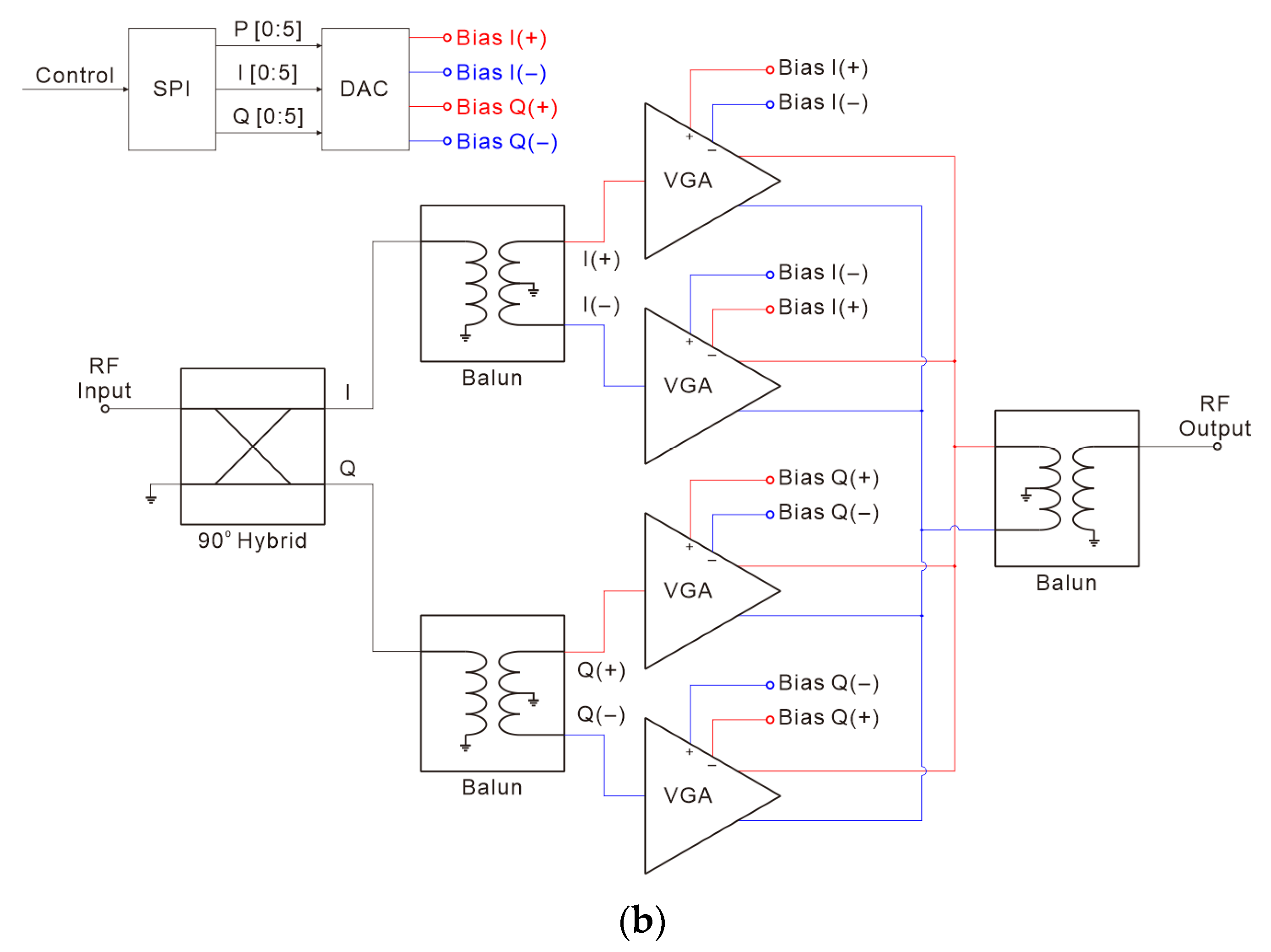
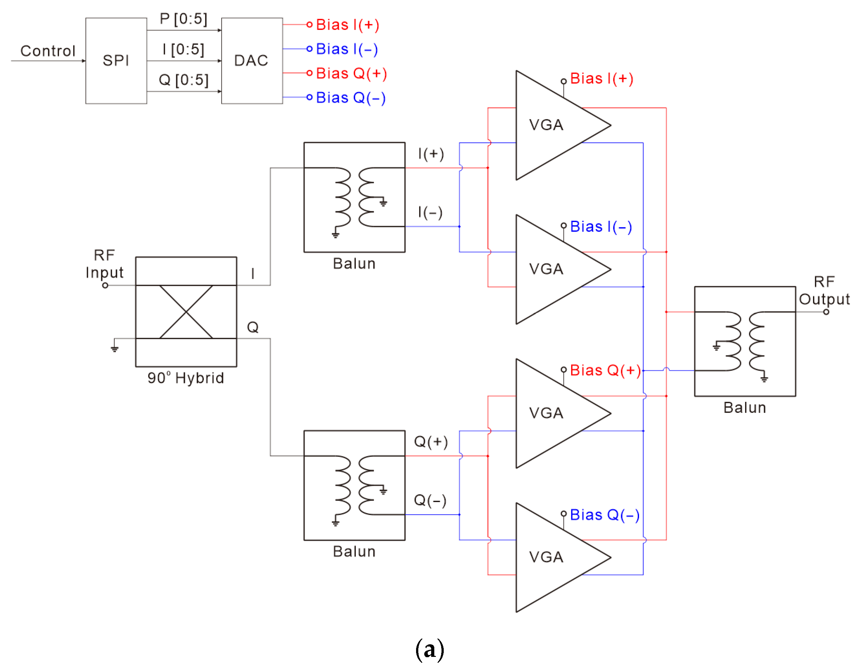
The VSPS method decomposes the input signal into four components, separated by 90°: in-phase plus (I+), in-phase minus (I−), quadrature plus (Q+), and quadrature minus (Q−). Then, the magnitude of each signal is amplified or attenuated using a VGA or Variable Attenuator, and the signals are combined to realize phase shifting. The operation principle is illustrated in Figure 1a,b.

Figure 1.
A block diagram of the (a) Gilbert cell-based VSPS and (b) current-steering-based VSPS.
Previous CMOS-based VSPS implementations have often adopted a common source Gilbert cell structure [,,], conceptually depicted in Figure 1a. However, these designs suffered from large losses, as the transistor limitations at high frequencies led to insufficient gains. To address this issue, this work proposes a phase shifter using a cascode amplifier-based current-steering VGA, as shown in Figure 1b, and compares it with the Gilbert cell-based structure. As a result, the proposed phase shifter achieved a 4.4 dB gain improvement over the Gilbert cell-based structure at 140 GHz.
The remainder of this paper is organized as follows. Section 2 describes the structure and operation of the VGA unit used to implement the two types of VSPSs. Section 3 presents the design methodology of the VSPS based on the proposed VGA, including the signal distribution and combination networks such as the balun and 90° hybrid coupler. Section 4 compares and analyzes the simulation results of the two phase shifters.
2. Comparison of Gilbert Cell and Current-Steering Variable Gain Amplifier
This work focuses on improving the gain of a vector-sum phase shifter by employing variable-gain amplifiers. Since the CMOS process inherently limits the gain at high frequencies, a method was sought to achieve higher gains while maintaining control simplicity. Two implementations were compared: one using a Gilbert cell structure and the other using current-steering.
2.1. Conventional Gilbert Cell-Based VGA Design
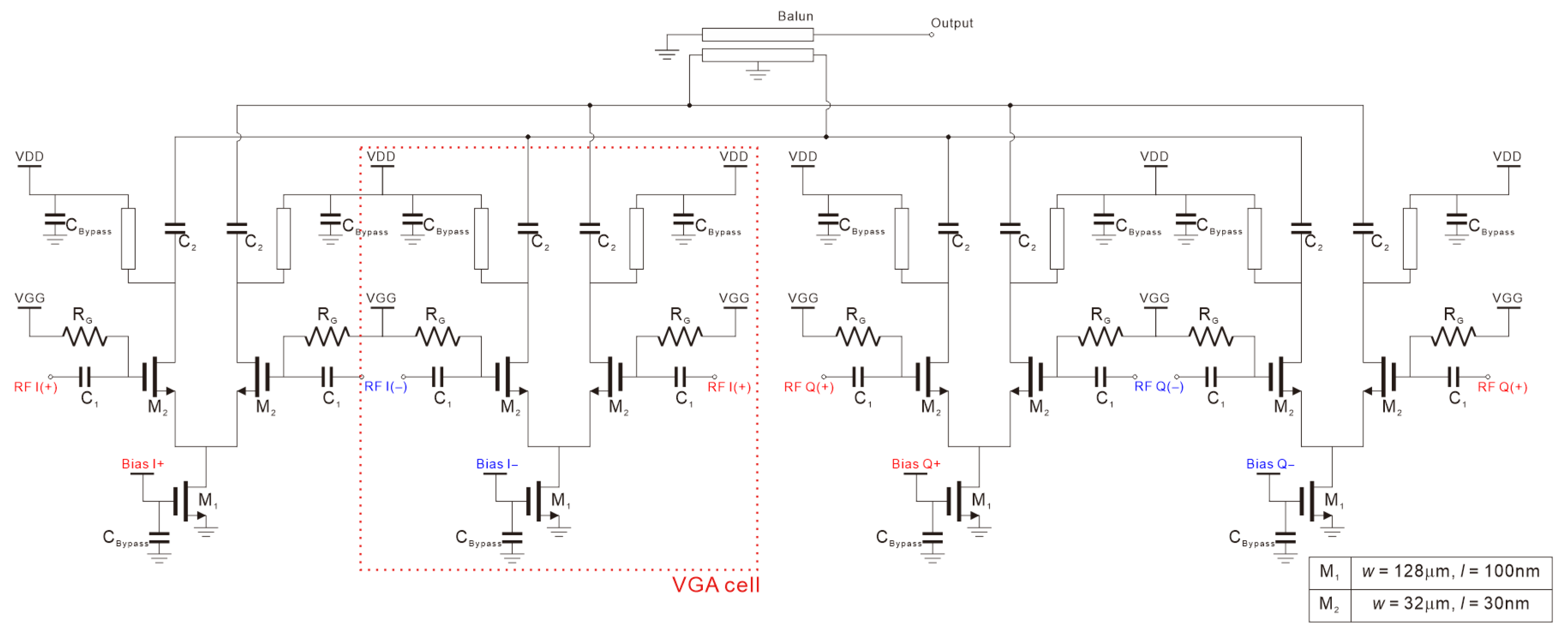
Figure 2 illustrates the in-phase section of the Gilbert cell-based VGA only. Bias I+ and Bias I−, converted into voltage levels by the current DAC, are applied to the gate of the M1 transistor and function as tail current sources []. By controlling the current of each tail branch through the DAC, the total output current remains constant. As a result, even if the gain of each node varies, the impedance of the output stage remains nearly constant.
Figure 2.
Schematic of the Gilbert cell-based VGA.
2.2. High-Gain Current-Steering VGA Design
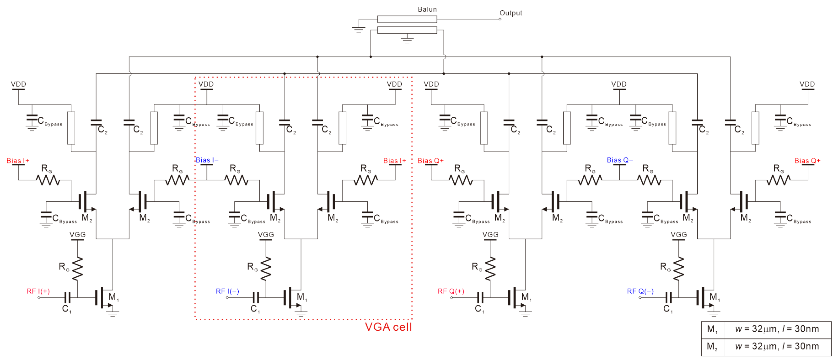
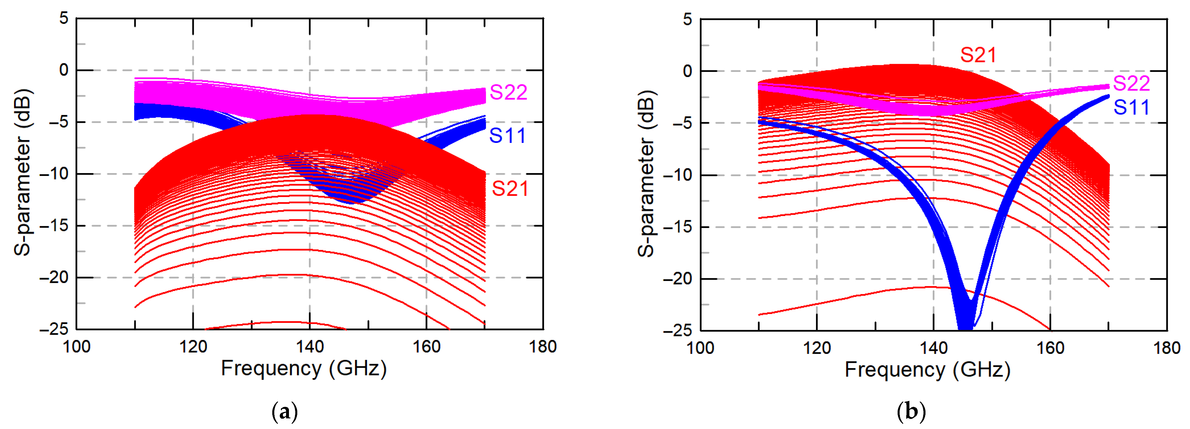
As shown in Figure 3, the proposed VGA replaces the conventional common-source amplifier with a cascode amplifier biased by a tail current source []. In this configuration, the input signal is applied to the gate of M1. In the previous design, the gain was controlled by adjusting the tail current; however, in the proposed cascode topology, the gain is tuned by varying the bias voltage of the common-gate (CG) amplifier. The performance improvement is shown in Figure 4, where the VGA gain increases by approximately 2.5 dB. In this configuration, the current through M1 remains constant, and the upper and lower transistors operate alternately, resulting in a nearly constant output impedance even when the gain changes.
Figure 3.
Schematic of current-steering VGA.
Figure 4.
Simulated S-parameter of (a) Gilbert cell-based VGA and (b) current-steering VGA.
3. Proposed Phase Shifter Design Using Dual VGAs
3.1. DAC for Gilbert Cell-Based Amplifier
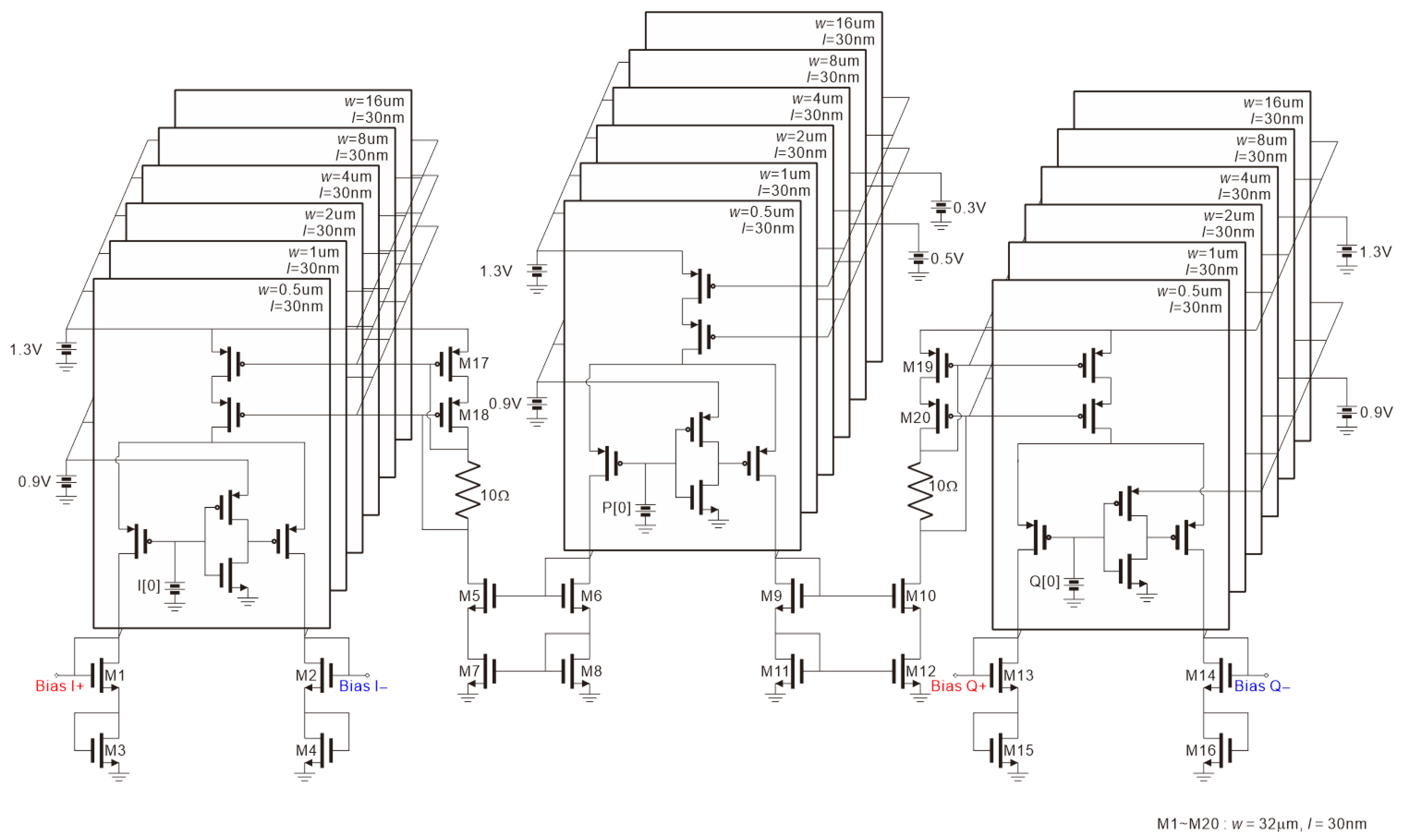
The DAC controlling each VGA in the phase shifter was implemented as a current-steering DAC. The basic architecture was adopted from a previously published VSPS design [,], while the transistor widths and lengths were optimized and modified to suit the 28 nm CMOS process. The applied digital control signals were converted into complementary logic levels through inverters to generate differential currents. These currents, produced by unit cells composed of transistors with scaled W/L ratios (×1, ×2, …, ×32), were summed to control both the phase and gain. The DAC receives 18-bit digital inputs: P [0:5], I [0:5], and Q [0:5] [,]. This 18-bit bus was mapped to an effective 13-bit control scheme. The eight bits for the phase control were composed of the six-bit P [0:5] for fine-tuning and two bits (derived from the I/Q buses) for quadrant selection. The five bits for gain control were implemented by sharing the remaining bits on the I and Q buses. As a result, the total number of effective control bits was 13, and 8192 simulation cases were generated, which are described in Section 4.
3.2. DAC for Current-Steering Amplifier
To drive the proposed current-steering VGA, the DAC structure was further modified from the reference design to accommodate the cascode amplifier topology. As illustrated in Figure 5, the bias values were carefully optimized to match the increased number of transistors, and device parameters were adjusted to ensure stable operation at D-band frequencies.
Figure 5.
The schematic of the DAC used for the current-steering phase shifter.
3.3. I/Q Generator
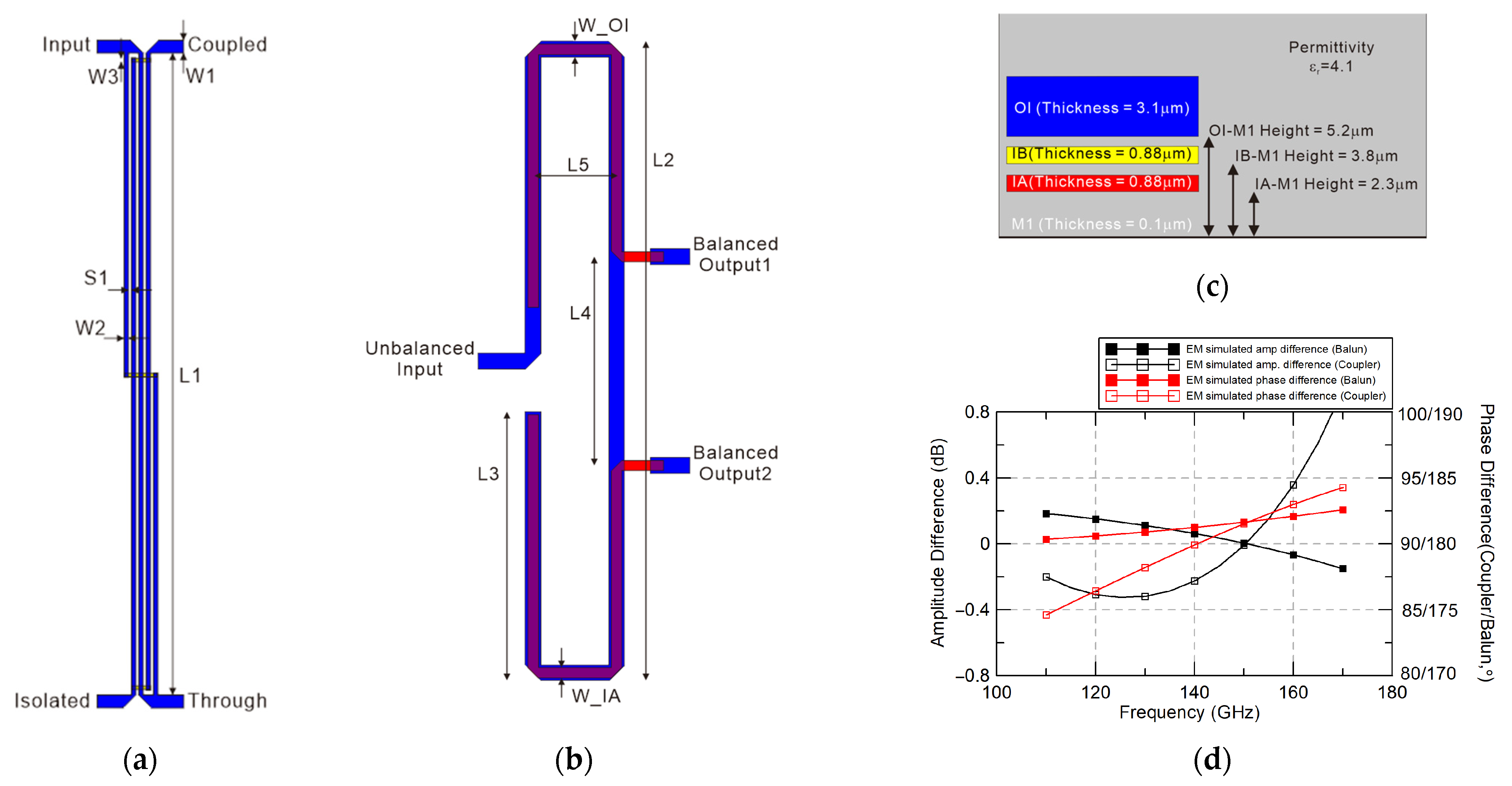
The quadrature hybrids in Figure 1 have been implemented as a Lange coupler. They generate the four signals, I+, I−, Q+, and Q−. The Lange coupler is implemented using OI and IB metal layers, as shown in Figure 6a,c and Table 1 with the central bridge connected by vias. As simulated in Figure 6d, the coupler exhibits a phase difference of 84.5–94.3° and a maximum magnitude imbalance of 0.93 dB over 110–170 GHz.
Figure 6.
(a) Layout of Lange coupler. (b) Layout of the Marchand balun. (c) Process cross-section. (d) EM-simulated amplitude and phase differences in Lange coupler and Marchand balun.
Table 1.
Design parameters of the Lange coupler and Marchand balun.
The baluns in Figure 1 are implemented as Marchand baluns using OI and IA layers, as shown in Figure 6b,c, and Table 1. Simulation results in Figure 6d indicate a phase difference of 180.3–182.5° and a maximum magnitude imbalance of 0.2 dB across the 110–170 GHz band. While an additional matching network is required to interface the baluns with the VGAs, this configuration offers broadband performance and structural simplicity, making it a suitable choice for the proposed design [].
3.4. Integrated Phase Shifter Design
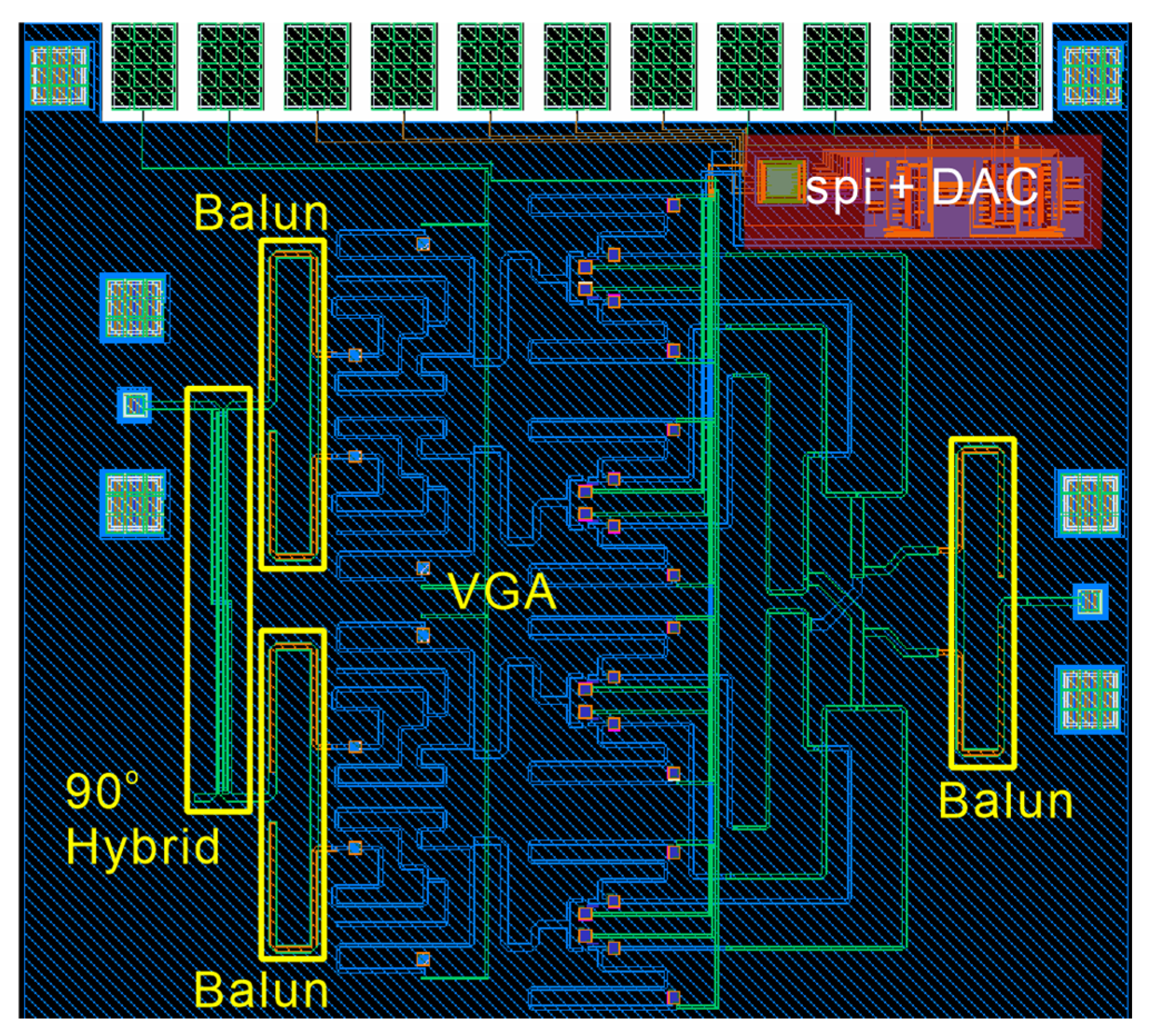
The circuits described above were combined to implement two simulated phase shifters. An I/Q generator was realized using one Lange coupler and two baluns, providing four signals to four VGAs. The bias inputs of the amplifiers were controlled by an 18-bit DAC model in simulation, which converts the digital control words into analog bias voltages for each VGA. Figure 7 shows the layout of the complete phase shifter circuit.
Figure 7.
Layout of total phase shifter.
4. Simulation Results for the Proposed Phase Shifter
The sensitivity of the gain to bias voltage variations in the proposed circuit was analyzed through layout simulations. For the 150 GHz Gilbert cell-based phase shifter, the variation in S21 with respect to the VDD was very small, within approximately 0.002 dB/mV (VDD = 0.8–1.5 V). The gain variation with respect to the VGG was also low, about 0.001 dB/mV at a VGG = 0.8 V, indicating that high precision in the bias setting is not required. However, due to transistor limitations, VDD = 1.0 V and VGG = 0.8 V were used. For the 140 GHz current-steering phase shifter, the gain variation with the VDD was similarly small, but it exhibited a relatively higher sensitivity to the VGG. At the point where the gain reaches its maximum, S21 decreased by approximately 0.2 dB when the VGG varied by 50 mV. Therefore, to maintain optimal gain performance, the VGG bias voltage must be precisely adjusted. Considering the potential voltage drop caused by parasitic resistance rather than the voltage increase, the circuit was operated with a VDD = 1.3 V and a VGG = 0.57 V.
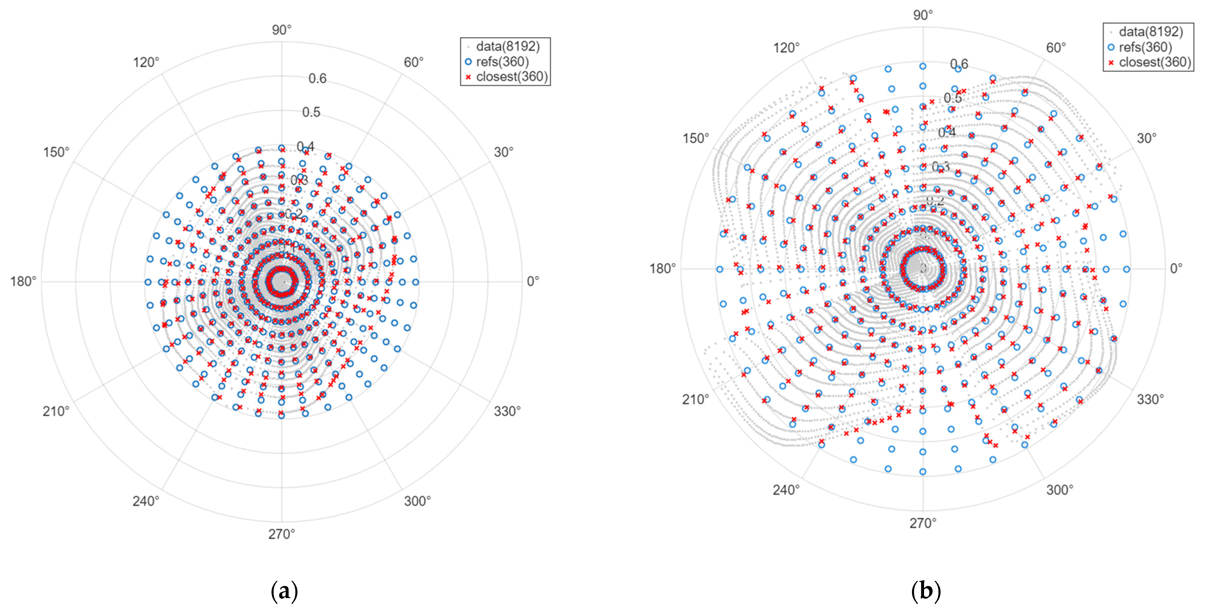
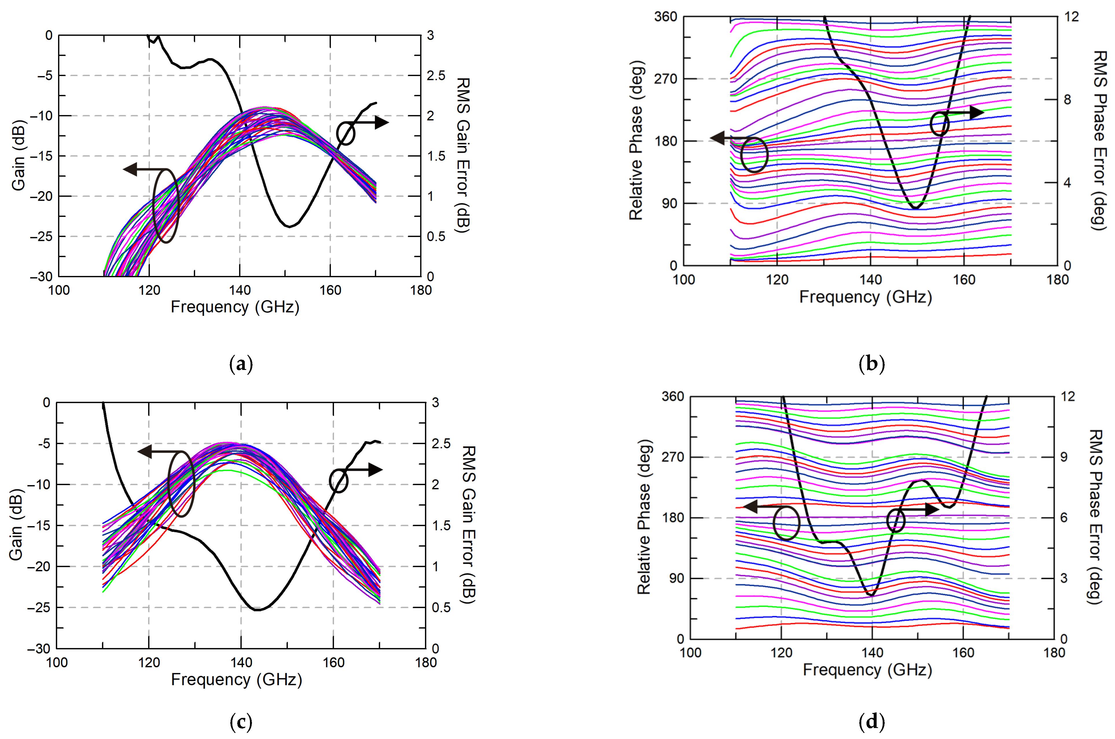
Based on the circuits described in Section 2 and Section 3, two phase shifters were implemented with different VGA designs. The simulation results are summarized in Figure 8 and Figure 9. Figure 8 shows polar plots obtained using 5-bit gain and 8-bit phase control. A total of 8192 simulated data points are shown in gray, with reference points at 10° intervals in blue, and the points closest to the references highlighted in red. The Gilbert cell-based phase shifter (Figure 8a) exhibited a maximum gain of −9.5 dB, whereas the current-steering phase shifter (Figure 8b) achieved −5.1 dB. Although the current-steering phase shifter is expected to achieve −3.7 dB with DAC or VGA optimization, the present setup yields −5.1 dB due to coarse phase intervals and magnitude errors.
Figure 8.
Simulated polar plot of the (a) Gilbert cell-based phase shifter S21 at 150 GHz and (b) current-steering phase shifter S21 at 140 GHz.
Figure 9.
(a) Simulated gain and RMS gain error of the Gilbert cell-based phase shifter. (b) Simulated relative phase of 36 states and RMS phase error of the Gilbert cell-based phase shifter. (c) Simulated gain and RMS gain error of the current-steering phase shifter. (d) Simulated relative phase of 36 states and RMS phase error of the current-steering phase shifter.
Figure 9 presents the simulated results of 36 points at 10° intervals under maximum gain conditions, along with RMS gain and phase errors across 360 points. The RMS errors in Figure 9 represent the simulated system-level performance assuming a Look-Up Table (LUT)-based control scheme. The 8192 data points (shown in Figure 8) serve as the characterized database for this LUT. For each of the 360 reference states, the optimal control setting was selected from this database by finding the point that minimizes the error vector (i.e., the closest point). This method mimics the practical operation of a digitally assisted phase shifter selecting the best available analog state. The Gilbert cell-based and current-steering phase shifters achieved RMS gain errors of approximately 2 dB and 1.3 dB and RMS phase errors of 6° and 4.8° over the 140–157 GHz and 129–144 GHz frequency bands, respectively.
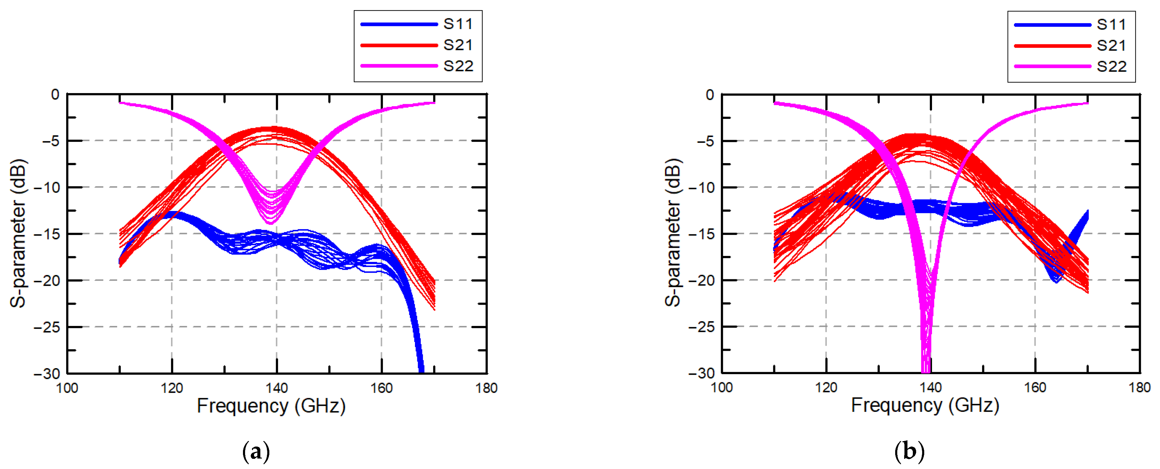
Figure 10 compares the schematic-level and post-layout simulation results of the current-steering-based phase shifter to validate the impact of parasitic effects. The post-layout simulation (Figure 10b) exhibits an overall gain degradation of approximately 2–3 dB and a slight shift in the peak frequency compared with the schematic-level result (Figure 10a). These variations primarily originate from the parasitic effects at 140 GHz, which are accurately captured by the post-layout extraction.
Figure 10.
(a) Schematic simulation result of current-steering-based phase shifter (phase control bias sweep). (b) Layout simulation result of current-steering-based phase shifter (phase control bias sweep).
Table 2 summarizes the performance of the proposed variable-gain vector-sum phase shifter and compares it with recently reported CMOS-based D-band phase shifters. The proposed design integrates a passive I/Q generator composed of a Lange coupler and a Marchand balun and employs two types of VGAs. As a result, the phase shifter achieves low RMS gains and phase errors while maintaining a wide gain control range. Compared with existing CMOS-based implementations, it also provides a higher gain and improved phase accuracy without the need for additional buffer amplifiers.
Table 2.
List of D-band phase shifter performance comparisons.
5. Conclusions
In this work, a vector-sum phase shifter operating in the D-band was implemented and analyzed using two different VGA architectures: the conventional Gilbert cell-based VGA and a proposed cascode current-steering VGA. The proposed phase shifter achieved full 0–360° phase control with stable gain characteristics. Simulation results demonstrated that the current-steering implementation improved the gain by 4.4 dB, achieved a 15-GHz bandwidth, and maintained low RMS gain and phase errors, which demonstrates its suitability for integration into future D-band CMOS phased array systems. Future work will focus on fabricating the chip and conducting measurements to experimentally validate the proposed architecture. These results confirm the feasibility of VSPS architectures with current-steering VGAs as a promising solution for high-frequency phased array systems in beyond 5G and 6G applications.
Author Contributions
Methodology, J.C.; Software, J.C. and J.-H.L.; Validation, J.C.; Data curation, J.C.; Writing—original draft, J.C.; Writing—review and editing, J.C. and J.-H.L.; Visualization, J.C.; Supervision, M.K. All authors have read and agreed to the published version of the manuscript.
Funding
This work was supported by the Institute of Information and Communications Technology Planning and Evaluation (IITP) grant funded by the Korean government (MSIT) (2021-0-00260, Research on LEO Inter-Satellite Links).
Institutional Review Board Statement
Not applicable.
Informed Consent Statement
Not applicable.
Data Availability Statement
The raw data supporting the conclusions of this article will be made available by the authors on request.
Acknowledgments
The authors would like to thank the IC Design Education Center (IDEC), Korea, for the chip fabrication and EDA tool support.
Conflicts of Interest
The authors declare no conflict of interest.
References
- Frecassetti, M.G.L.; Sevillano, J.F.; del Rio, D.; Saglam, M.I.; Lamminen, A.; Ermolov, V. D-Band Backhaul and Fronthaul Solutions for 5G Radio Access Network. In Proceedings of the 2022 52nd European Microwave Conference (EuMC), Milan, Italy, 27–29 September 2022; Volume 52, pp. 772–775. [Google Scholar]
- Wang, H.; Guo, H.; Zhang, X.; Chi, T. A Packaged D-Band Transmitter with a Multifeed Lens Antenna Achieving 25.3 dBm Single-Element EIRP for 2-D Scalable Arrays. In Proceedings of the 2025 IEEE Custom Integrated Circuits Conference (CICC), Boston, MA, USA, 13–17 April 2025; pp. 1–3. [Google Scholar]
- Li, S.; Zhang, Z.; Rupakula, B.; Rebeiz, G.M. An Eight-Element 140-GHz Wafer-Scale IF Beamforming Phased-Array Receiver with 64-QAM Operation in CMOS RFSOI. IEEE J. Solid-State Circuits 2022, 57, 385–399. [Google Scholar] [CrossRef]
- Cho, M.K.; Baek, D.; Kim, J.G. An X-Band 5 Bit Phase Shifter with Low Insertion Loss in 0.18 μm SOI Technology. IEEE Microw. Wireless Compon. Lett. 2012, 22, 648–650. [Google Scholar] [CrossRef]
- Gu, P.; Zhao, D.; You, X. Analysis and Design of a CMOS Bidirectional Passive Vector-Modulated Phase Shifter. IEEE Trans. Circuits Syst. I 2021, 68, 1398–1408. [Google Scholar] [CrossRef]
- Li, W.T.; Chiang, Y.C.; Tsai, J.H.; Yang, H.Y.; Cheng, J.H.; Huang, T.W. 60-GHz 5-bit Phase Shifter with Integrated VGA Phase-Error Compensation. IEEE Trans. Microw. Theory Tech. 2013, 61, 1224–1235. [Google Scholar] [CrossRef]
- Li, T.W.; Wang, H. A Millimeter-Wave Fully Integrated Passive Reflection-Type Phase Shifter with Transformer-Based Multi-Resonance Loads for 360° Phase Shifting. IEEE Trans. Circuits Syst. I 2018, 65, 1406–1419. [Google Scholar] [CrossRef]
- Zhang, Z.; Yang, M.; Xie, Q.; Wang, Z. A D-band quadrature-hybrids-based 5-bit vector-modulated phase shifter with low RMS phase error. Electron. Lett. 2022, 58, 717–719. [Google Scholar] [CrossRef]
- Wang, S.; Park, J.; Hong, S. A K-Band Variable-Gain Phase Shifter Based on Gilbert-Cell Vector Synthesizer with RC-RL Poly-Phase Filter. IEEE Microw. Wireless Compon. Lett. 2021, 31, 393–396. [Google Scholar] [CrossRef]
- So, C.; Sung, E.T.; Hong, S. A 60-GHz Variable-Gain Phase Shifter with an Active RL Poly-Phase Filter. IEEE Trans. Microw. Theory Tech. 2023, 71, 593–601. [Google Scholar] [CrossRef]
- Sung, E.-T.; Wang, S.; Hong, S. A 60-GHz Polar Vector Modulator with Lookup Table-Based Calibration. IEEE Microw. Wireless Compon. Lett. 2021, 31, 572–574. [Google Scholar] [CrossRef]
- Najmussadat, M.; Ahamed, R.; Varonen, M.; Parveg, D.; Kantanen, M.; Halonen, K.A.I. 220–240-GHz High-Gain Phase Shifter Chain and Power Amplifier for Scalable Large Phased-Arrays. IEEE Access 2023, 11, 23565–23577. [Google Scholar] [CrossRef]
- So, C.; Sung, E.-T.; Hong, S. A 60-GHz Variable Gain Phase Shifter Based on Body Floated RF-DAC Structure. IEEE Trans. Circuits Syst. II 2022, 69, 4749–4753. [Google Scholar] [CrossRef]
- Rao, S.G.; Cressler, J.D. A D-Band Reflective-Type Phase Shifter Using a SiGe PIN Diode Resonant Load. IEEE Microw. Wireless Compon. Lett. 2022, 32, 1191–1194. [Google Scholar] [CrossRef]
- Yishay, R.B.; Elad, D. D-Band 360° Phase Shifter with Uniform Insertion Loss. In Proceedings of the 2018 IEEE/MTT-S International Microwave Symposium—IMS, Philadelphia, PA, USA, 10–15 June 2018; pp. 868–870. [Google Scholar]
- Karakuzulu, A.; Eissa, M.H.; Kissinger, D.; Malignaggi, A. Broadband 110–170 GHz True Time Delay Circuit in a 130-nm SiGe BiCMOS Technology. In Proceedings of the 2020 IEEE/MTT-S International Microwave Symposium (IMS), Los Angeles, CA, USA, 4–6 August 2020; pp. 775–778. [Google Scholar]
- Abbasi, M.; Lee, W. A D-band Calibration-Free Passive 360° Phase Shifter with 1.2°RMS Phase Error in 45 nm RFSOI. In Proceedings of the 2023 IEEE Radio Frequency Integrated Circuits Symposium (RFIC), San Diego, CA, USA, 11–13 June 2023. [Google Scholar]
- Kim, I.; Koo, H.; Kim, W.; Hong, S. A D-Band Differential Phase Shifter Based on a Transmission Delay Line with Variable Inductors and Capacitors. IEEE Microw. Wireless Technol. Lett. 2025, 35, 59–62. [Google Scholar] [CrossRef]
- Zhang, Z.; Yang, M.; Geng, X.; Wang, K.; Xie, Q.; Wang, Z. A 0.0325-mm2 114-to-147-GHz 6-Bit Passive Vector-Modulated Phase Shifter with MN-Embedded Isolated Power Combiner Achieving <3.7° RMS Phase Error in 65-nm CMOS. IEEE Trans. Circuits Syst. I 2023, 70, 4394–4405. [Google Scholar]
- Testa, P.V.; Carta, C.; Ellinger, F. A 160–190-GHz Vector-Modulator Phase Shifter for Low-Power Applications. IEEE Microw. Wirel. Compon. Lett. 2020, 30, 86–89. [Google Scholar] [CrossRef]
- del Rio, D.; Gurutzeaga, I.; Berenguer, R.; Huhtinen, I.; Sevillano, J.F. A Compact and High-Linearity 140-160 GHz Active Phase Shifter in 55 nm BiCMOS. IEEE Microw. Wireless Compon. Lett. 2021, 31, 157–160. [Google Scholar]
Disclaimer/Publisher’s Note: The statements, opinions and data contained in all publications are solely those of the individual author(s) and contributor(s) and not of MDPI and/or the editor(s). MDPI and/or the editor(s) disclaim responsibility for any injury to people or property resulting from any ideas, methods, instructions or products referred to in the content. |
© 2025 by the authors. Licensee MDPI, Basel, Switzerland. This article is an open access article distributed under the terms and conditions of the Creative Commons Attribution (CC BY) license (https://creativecommons.org/licenses/by/4.0/).