Abstract
Nowadays, Graphical Processor Units (GPUs) are a great technology to implement Artificial Intelligence (AI) processes; however, a challenge arises when the inclusion of a GPU is not feasible due to the cost, power consumption, or the size of the hardware. This issue is particularly relevant for portable devices, such as laptops or smartphones, where the inclusion of a dedicated GPU is not the best option. One possible solution to that problem is the use of a CPU with AI capabilities, i.e., parallelism and high performance. In particular, RISC-V architecture is considered a good open-source candidate to support such tasks. These capabilities are based on vector operations that, by definition, operate over many elements at the same time, allowing for the execution of SIMD instructions that can be used to implement typical AI routines and procedures. In this context, the main purpose of this proposal is to develop an ASIC Vector Engine RISC-V architecture compliant that implements a minimum set of the Vector Extension capable of the parallel processing of multiple data elements with a single instruction. These instructions operate on vectors and involve addition, multiplication, logical, comparison, and permutation operations. Especially, the multiplication was implemented using the Vedic multiplication algorithm. Contributions include the description of the design, synthesis, and validation processes to develop the ASIC, and a performance comparison between the FPGA implementation and the ASIC using different nanometric technologies, where the best performance of 110 MHz, and the best implementation in terms of silicon area, was achieved by 7 nm technology.
1. Introduction
Artificial Intelligence (AI) has rapidly emerged as a critical driver of innovation, requiring hardware solutions capable of executing highly parallel and data-intensive workloads. While Graphics Processing Units (GPUs) have become the preferred platform for AI acceleration due to their superior parallel processing capabilities, their integration in cost-sensitive, power-constrained, and space-limited environments, such as portable and embedded devices, remains challenging. The growing demand for on-device AI processing necessitates alternative approaches that balance computational power with efficiency and integration constraints [1,2].
Central Processing Units (CPUs) enhanced with vector operations, also known as Single Instruction, Multiple Data (SIMD) extensions, present a promising solution. These operations enable substantial improvements in throughput by simultaneously applying instructions across multiple data elements, partially bridging the performance gap between CPUs and GPUs for AI workloads. In this context, RISC-V continues to reaffirm itself as an efficient and scalable alternative. A great survey that provides a RISC-V hardware architecture background, challenges, and a quantitative taxonomy of RISC-V SoC can be found in [3]. In particular, the RISC-V Vector Extension offers a flexible and open-source foundation for building efficient proposals like [4], where a microcontroller uses Vector Extension combined with RV32E for meeting area and power for IoT applications. At the chip level, there are some remarkable projects like [5,6,7], where the authors explore a Vector Extension for 64-bit RISC-V, focusing on high-performance computing (HPC) with full hardware support for floating-point operations in 32 and 64 formats. These approximations are sometimes categorized as scalable RISC-V vector (RVV) processors [8] and are oriented to HPC workloads [9] with scalable AI-capable hardware [10,11]. Likewise, ref. [12] applies the register remapping technique, used to overcome limitations imposed by a limited number of architectural registers, specifically for vector processing, and proposes a new scheme of a hardware reduction tree for RVV reduction operations that are crucial for digital signal processing and neural network algorithms. In addition, an interesting computing-based high-performance paradigm oriented to AI applications is heterogeneous computing, where a general-purpose processor and a hardware unit can be combined to accelerate arithmetic operations [13].
This proposal investigates the minimum hardware footprint required to implement a core subset of vector instructions essential for AI and data parallel applications, including arithmetic, logical, comparison, and permutation operations. Additionally, it evaluates the maximum achievable operating frequency of the vector processing unit synthesized with ASIC technology. Through this dual analysis, this research study aims to assess the feasibility of lightweight Vector Engines that deliver a competitive performance in constrained environments without the overhead of full-scale GPU integration [14].
2. Materials and Methods
2.1. Vector Instructions in RISC-V Architecture
The vector operations implemented in this work adhere strictly to the official RISC-V Vector Extension specification [15]. All instructions follow the behavior and structure as defined in the RISC-V Vector Extension manual, ensuring compliance with the standard’s operational semantics.
However, due to the data processing scope, i.e., mainly arithmetic and logical instructions, not all the instructions described in the specification were implemented. The implementation comprises a basic subset of vector operations, explicitly focusing on fundamental arithmetic, logical, and permutation instructions. These were selected to enable essential vector processing capabilities and to demonstrate functional support for vectorized computation.
It is important to note that several categories of instructions, such as memory operations, fixed-point arithmetic, floating-point arithmetic, and vector configuration mechanisms, are intentionally excluded from this implementation. The choice to focus on a minimal but functional core subset of instructions reflects a balance between feasibility and practical demonstrations of vector capabilities.
The list of implemented instructions and the category of each one is provided in Appendix A.
2.2. Design of a Vector Engine for RISC-V Architecture
This proposal is specifically focused on the implementation of vector instructions, with particular emphasis on their decoding and execution. Consequently, only the components required for decoding and executing vector instructions are included in the proposed architecture. The fetching of instructions, handling, and execution of non-vector instructions, as well as memory access operations, are beyond the scope of this work. These aspects are assumed to be managed externally or are abstracted for the purpose of this implementation. This scope restriction allows for a concentrated effort on the correct and efficient realization of vector functionality.
The top module of the Vector Engine is shown in Figure 1 and the light blue box represents the Vector Engine while the blocks outside the rectangle and colored in gray are blocks that are not implemented by the Vector Engine and should be implemented externally.
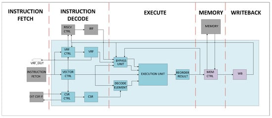
Figure 1.
Vector engine architecture.
To maintain design simplicity, a classic five-stage pipelining scheme is adopted: Fetch, Decode, Execute, Memory, and Write Back. This decision reduces architectural complexity and centers the effort on the core functionality of vector instruction handling. The adoption of this standard five-stage structure facilitates potential integration with other open-source RISC-V cores that follow the same pipelining scheme, thereby promoting modularity and interoperability. However, this design choice also imposes limitations, particularly in terms of maximum achievable operating frequency. Particularly, the Execute stage can become a bottleneck due to its computational complexity. Table 1 shows the actions performed during each stage.

Table 1.
Pipeline stages.
The incoming instruction is read and analyzed during the Decode stage to determine whether it corresponds to a vector instruction. If the instruction is identified as a vector operation, the appropriate control signals are asserted to activate the corresponding vector execution units. In contrast, if the instruction is not part of the supported vector subset, it is effectively ignored, and all execution units are disabled to prevent unintended activity.
Simultaneously, during this stage, the required operands are retrieved from the register file. Additionally, relevant control and status registers (CSRs) are accessed to determine the specific variant or configuration of the operation to be executed.
At the beginning of the Execute stage, the values of the control and status registers (CSRs) accessed during the Decode stage are interpreted. These include key registers such as VSTART, VLEN, and VTYPE, which determine the vector operation’s starting index, active vector length, and data size, respectively. If the instruction is a masked operation, the corresponding vector mask (VMASK) is also retrieved and decoded.
Using this information, the control logic evaluates the execution conditions for each element in the vector. A write enable mask is generated accordingly, indicating which bytes or elements are allowed to be updated during the Write Back stage. This selective enabling mechanism ensures that only the active elements based on the current vector configuration and mask settings are modified, while inactive elements remain unchanged.
Concurrently with the decoding of the CSR values during the Execute stage, the bypass unit becomes active. This unit serves a dual purpose. First, it performs traditional data forwarding (bypassing) by sourcing the most recent operand values from either the Memory or Write Back stages, thereby resolving data hazards and eliminating unnecessary stalls due to operand dependencies.
Second, the bypass unit is responsible for normalizing the operand format before they are fed into the vector ALU. If an operand originates from an immediate value or from the scalar integer register file, the unit performs appropriate transformations such as sign extension and element replication. These transformations ensure that all operands, regardless of their source, are presented to the execution units in a uniform, vector-ready format. This abstraction simplifies the ALU design and guarantees consistent behavior across all supported operand types and sources.
The execution units are primarily divided into three specialized ALUs: arithmetic, logical, and permutation.
2.2.1. Logical ALU
The logical ALU is responsible for executing all bitwise logical operations, shift operations, and mask processing. It is composed of modular 8-bit logic blocks that implement the fundamental bitwise operations: AND, OR, and XOR. These blocks are interconnected through a configurable network of multiplexers, allowing dynamic reconfiguration based on the type of operation. This architecture enables the reuse of the same hardware blocks to support multiple functional modes, including standard bitwise operations, bitwise reductions, and mask manipulation. For shift operations, a dedicated logic block is used, based on a modified barrel shifter design. Figure 2 shows the register transfer level (RTL) schematic of the logical ALU.
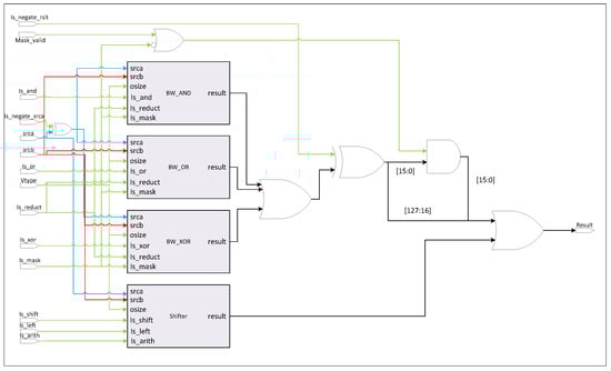
Figure 2.
Logic ALU.
2.2.2. Arithmetic ALU
The arithmetic ALU is dedicated to executing vector arithmetic operations such as addition, subtraction, comparisons, and multiplication. Addition, subtraction, and comparison operations are implemented using shared hardware resources.
Similar to the logical ALU, the arithmetic ALU is built around modular 8-bit adder blocks. These blocks are connected through a flexible multiplexer network that allows dynamic configuration based on the operation type. To support varying operand widths, the carry outputs of the adders can be chained together, effectively increasing the datapath width. For normal element-wise operations, the adders are configured to operate in parallel, while for reduction operations, the same blocks can be cascaded in series.
Comparison operations are implemented using the subtraction logic. A subtraction is performed between operands, and the resulting condition flags (such as zero, sign, and carry/borrow) generated by the adder blocks are evaluated to determine the comparison outcome. Figure 3 shows the RTL schematic of the vector adder module.
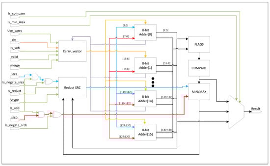
Figure 3.
Vector adder.
In the case of the multiplier, it has its own independent logic. The multiplier is based on the Vedic Mathematics, which is an ancient Indian mathematical system rediscovered and founded by Sri Bharati Krishna Tirthaji between 1911 and 1918. It is based on sixteen sutras. One of them is the Urdhava Tiryakbhyam Sutra, which means vertically and crosswise calculation, and it is the sutra where the Vedic multiplier is based [16]. The Urdhava Tiryakbhyam method is used to multiply two decimal numbers; it multiplies the digits of the number vertically and crosswise to generate partial products and then adds the partial products to get the final result, as shown in Figure 4. The vectorized multiplication is given by
where the suffix T and the suffix U denote the tens and the unit digits of the number, respectively. For example, if A = 73, then AT = 7 and AU = 3. This sutra can be extended to binary numbers; the numbers can be divided by half by applying a similar procedure to decimal numbers.
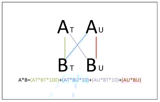
Figure 4.
Urdhava Tiryakbhyam method for Vedic multiplier.
One of the key advantages of the Vedic multiplier architecture lies in its inherent ability to generate intermediate partial products that correspond directly to smaller operand sizes. In contrast, a conventional vector multiplication unit based on array multipliers typically requires a dedicated multiplier for each operand width—for example, eight 8-bit multipliers, four 16-bit multipliers, two 32-bit multipliers, and one 64-bit multiplier to support 8, 16, 32, and 64-bit operations. The Vedic approach, however, enables the use of a single multiplier unit to handle all these operand sizes efficiently. For instance, a 32-bit multiplication inherently produces four 16-bit partial products, two of which can directly serve as the result for a 16-bit multiplication. By incorporating a multiplexer at the output stage, the appropriate result can be selected directly from these internal partial products, eliminating the need for separate hardware units per operand width.
Compared to a conventional array multiplier, this design introduces only a modest area overhead of approximately 25%, while achieving significant performance gains. Empirical observations indicate that the Vedic multiplier can be up to three times faster than its array-based counterpart, making it an attractive solution for high-throughput vector processing with diverse operand widths. Figure 5 shows the RTL view of the Vedic multiplier used.
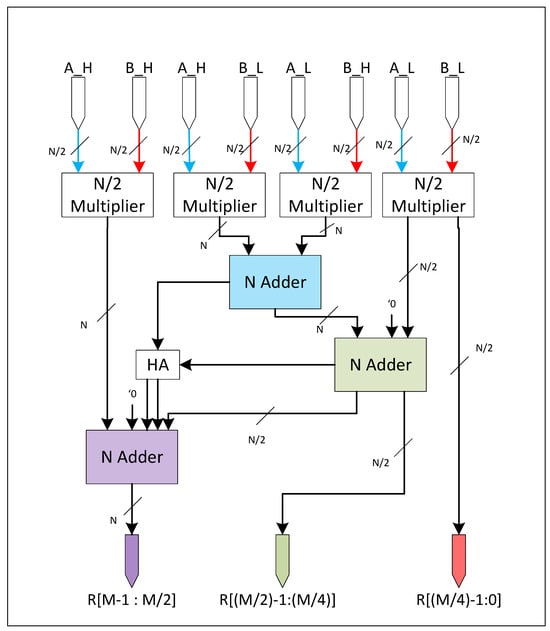
Figure 5.
Vedic multiplier.
2.2.3. Permutation ALU
The permutation ALU is architecturally streamlined, functioning primarily as a gating and routing unit for operand manipulation. Unlike the arithmetic or logical units, it performs no heavy computation internally. This simplicity is possible because the conversion logic, such as sign extension and the transformation from scalar to vector formats, is already handled by the bypass unit upstream.
When executing permutation-type operations, the ALU merely selects and forwards the appropriately pre-formatted operand provided by the bypass unit. In the case of scalar to vector conversions, this involves passing through the replicated and sign-extended value directly. For vector-to-scalar conversions, the process is reduced to a simple truncation of the most significant bits to obtain a scalar result.
2.3. Functional Validation of the Vector Engine
Figure 6 illustrates the validation architecture used for the Vector Engine. The upper section contains the UVM agents, each responsible for generating, monitoring, or driving specific signal domains. The lower block represents the RTL design under test (DUT). The yellow rectangles denote the virtual interfaces used to interconnect the RTL with the UVM verification environment.
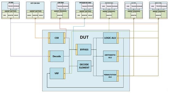
Figure 6.
Vector engine validation architecture.
The if_env agent generates valid vector instructions and drives them into the DUT for execution. Ext_csr_env sends commands to modify internal CSR registers of the DUT. Csr_env maintains a reference model of the CSR state to be used by the verification components. Integer_rf_env is a model of the integer register file that supplies scalar data inputs to the DUT. Vector_rf_env acts as a monitor and checker for the vector register file functionality.
Alu_env models the reference behavior of the execution units and verifies that all instructions are correctly computed. Finally, riscv-v_env oversees the full instruction flow, verifying its correctness from the Decode stage to the Write Back stage.
Each supported operation has its own test to verify its correctness. The test generates stimuli to execute all the supported variants of the instructions, including all the supported combinations of VTYPE, VLEN, and VSTART along with different mask registers. All the tests use the same structure to generate the stimuli; they are configured with the desired stimuli to be generated. First, the test initializes the vector register file with random data. Once all the registers have been initialized, the test starts sending different blocks of instructions, one block being one variant of the instruction, and the length of the block can be configured within the test. The test iterates over all the valid variants of the instruction and sends one block of instructions of each variant. Figure 7 shows the simulation of the VADD instruction, where the structure used by all the tests can be observed.
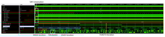
Figure 7.
VADD instruction simulation.
All the simulations were run using Vivado 2024.1 using a TCL script to run the tests in shell mode, saving the logs of the tests indicating if the test passes or fails, and the coverage database of the tests. The test is only set as PASS if there are no errors or fatal messages in the log file; if one error or fatal message is encountered, the test status is set to FAIL. Once all the tests were executed, the coverage databases were merged into a single database, and a Python script was executed. This script reads all the log files and indicates the final status of each test, indicating also if the regression passed or failed.
2.4. Synthesis for FPGA Prototype
One synthesis was performed aiming for an FPGA platform. The selected family was the ARTIX7 from XILINX, using the chip xc7a200tfbq676-2. This chip was selected since it is the chip with the most resources in the family ARTIX77 that can be implemented using the free license of the Vivado 2024.1 software that was used to perform the FPGA synthesis.
2.5. Synthesis for ASIC Implementation
An ASIC synthesis was also performed using 4 different ASIC platforms and open-source software. The software used to perform the synthesis is OpenROAD. OpenROAD is a fully autonomous RTL to GDSII flow for rapid design exploration and physical design implementation [17]. OpenROAD can be obtained from its official OpenROAD flow repository (https://github.com/The-OpenROAD-Project/OpenROAD-flow-scripts, accessed on 29 April 2025).
The synthesis was performed using the synthesis scripts provided by the repository. The scripts can be modified to perform fine-tuning, but they were used as they are presented in the original repository without modifying the scripts; just some configuration variables, like the clock period, the layers to route the design, and the core area, were modified to perform the synthesis according to the circuit’s necessities.
The repository also includes four open-source Process Design Kits (PDKs) that were used to synthesize the circuit.
The first PDK is the GF180MCU PDK. This is an open-source PDK that was developed by Global Foundries in collaboration with Google. The PDK provides the resources needed to enable the creation of designs manufactured at the Global Foundries facilities using its 180 nm process [18]. The PDK can be found in this repository: GF180 (https://github.com/google/gf180mcu-pdk?tab=readme-ov-file, accessed on 29 April 2025).
The second PDK is the SKY130 PDK. This open-source PDK is a collaboration between SkyWater Technology Foundry and Google. The PDK can be manufactured at SkyWater’s facilities using its 130 nm process [19]. The node used by this PDK is a 130 nm–180 nm hybrid technology. The PDK can be found in this repository: SKY130 (https://github.com/google/skywater-pdk, accessed on 29 April 2025).
The third PDK is the FREEPDK45 PDK. This PDK, unlike the previous PDK, is a generic 45 nm PDK that is not mapped to a technology or a fabrication node, which means that the circuit can not be fabricated using this PDK [20]. It was developed by the NC State University and can be obtained using SVN from this repository: FREEPDK45 (https://eda.ncsu.edu/freepdk/freepdk45/, accessed on 29 April 2025).
The last PDK is the ASAP7 PDK. This is an open-source academic PDK developed by Arizona State University and ARM using a FinFET 7 nm Technology. As the FREEPDK45, this PDK is only intended for research and academic purposes and can not be manufactured at any fabric [21]. The PDK can be found at this repository: ASAP7 (https://github.com/The-OpenROAD-Project/asap7_pdk_r1p7/tree/main, accessed on 29 April 2025).
3. Results
Beginning with the analysis of the multiplication unit, Table 2 presents a comparative evaluation between a conventional array-based multiplier and a Vedic multiplier. It is important to note that this table refers to standalone N-bit multipliers without support for vectorized operations. This comparison was conducted using the ASAP7 ASIC platform. The results reveal that for smaller operand widths, the performance difference between the two architectures is relatively minor. However, as the operand width increases, the performance gap becomes more significant, particularly in terms of speed. Starting at an 8-bit width, the Vedic multiplier demonstrates a 20% improvement in speed over its array-based counterpart. At a width of 128 bits, the performance advantage becomes even more pronounced, with the Vedic multiplier achieving speeds up to 3.6 times faster while incurring only a 50% increase in area. These results highlight the scalability and efficiency of the Vedic architecture for high-bit-width vector operations.
Table 2.
Scalar multiplier statistics.
The greatest advantage of the Vedic multiplier becomes evident when implementing the vector multiplication unit. In contrast, the array-based approach requires instantiating multiple separate multipliers to support various operand sizes, as illustrated in Figure 8. With the Vedic multiplier, only a single instance is needed, since operations with smaller operand widths can be directly obtained from the internally generated partial products. This is illustrated in Figure 9, which shows the instantiation of the Vedic multiplier, and in Figure 10, where the partial products used to derive the results for smaller widths are depicted.
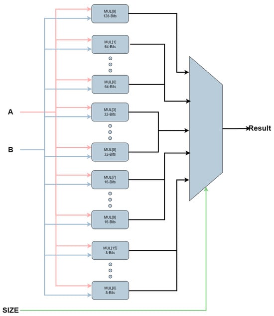
Figure 8.
Vector multiplier implemented using array multiplier.
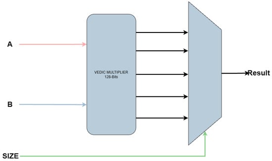
Figure 9.
Vector multiplier implemented using Vedic multiplier.
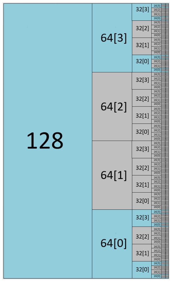
Figure 10.
Vedic internal partial products used to implement the vector multiplier.
Analyzing the vector multiplication unit, Table 3 presents a comparison between two implementations: one using the Vedic multiplier as a base multiplier and the second one using the array multiplier. The “MAX SIZE” field indicates the maximum supported operand width, which in this case is 128 bits. This implies support for operations of 8, 16, 32, 64, and 128 bits. In the case of the Vedic implementation, the results for the area and the maximum frequency were approximately the same values as those reported in Table 2, where only the multiplier was synthesized. The slight increase in area and the modest reduction in frequency are due to the addition of a multiplexer at the output stage, required to extract the correct partial result.
Table 3.
Vector multiplier statistics.
On the other hand, in the array-based implementation, the area doubles. This is because implementing a vector multiplier for a MAX SIZE of 128 bits requires the instantiation of one 128-bit multiplier (which determines the maximum frequency), two 64-bit multipliers, four 32-bit multipliers, eight 16-bit multipliers, and sixteen 8-bit multipliers.
It can be observed that using the Vedic multiplier as the base multiplier for the implementation of a vector multiplication unit improves both area and speed compared to an implementation based on an array multiplier. The Vedic-based design consumes only 88.6% of the area required by the array-based implementation while achieving a maximum frequency up to 3.4 times higher.
The synthesis of the vector execution unit was completed successfully using both an FPGA platform and four previously mentioned PDKs for ASIC implementation. Table 4 summarizes the synthesis results across these platforms, highlighting key metrics relevant to performance and area utilization.
Table 4.
Synthesis statistics.
For each platform, Table 4 reports the maximum operating frequency achieved (in MHz), the corresponding clock period (in nanoseconds), the number of combinational cells (or LUTs in the case of the FPGA), and the number of sequential cells (typically flip-flops or registers). In addition to cell counts, the table includes the area occupied by combinational logic, expressed both in absolute units and as a percentage of the total available area, as well as the area used by sequential logic.
Notably, the combinational cell count reflects only the cells required to implement the logic described in the RTL design. This excludes any additional logic introduced by the synthesis tool, such as buffers or optimization support logic. However, the area metrics do include all synthesized components, both designer-specified and tool-generated, providing a realistic view of the total silicon footprint.
For the detailed analysis, the ASAP7 platform was primarily used, as it yielded the best performance among the evaluated platforms. Although the SKY130 platform is manufacturable, it is based on an older 130 nm technology node, which results in a significantly larger area and lower performance. In contrast, ASAP7, while not manufacturable and only intended for academic research, is based on a modern 7 nm technology. Using ASAP7 allows for obtaining performance and area metrics that are more representative of what could be achieved using a commercial-grade 7 nm manufacturing process.
The synthesis results reveal that the design is heavily dominated by combinational logic, which accounts for approximately 90% of the total area, while sequential logic occupies the remaining 10%.
A significant contributor to the sequential logic area is the vector register file, which represents the largest portion of the instantiated flip-flops. Specifically, it comprises 4096 flip-flops, required to implement 32 vector registers, each 128 bits wide.
On the combinational side, the multiplier unit is the most resource-intensive block. It instantiates 50,723 combinational cells, which equate to approximately 53% of the total circuit area. This is consistent with expectations, as high bit-width multiplication operations demand a large number of logic gates for partial product generation and accumulation.
In terms of maximum operating frequency, the critical path bottleneck lies in the adder unit, although it is not the most resource-intensive component in terms of area or cell count. The adder instantiates 4057 combinational cells, consuming approximately 4% of the total area. However, it exhibits the deepest logic depth in the design, with a total of 165 logic levels along its critical path. This extensive logic depth significantly limits the achievable clock frequency and underscores the need for architectural optimization in this block.
Interestingly, the multiplier, although much larger in terms of cell count, instantiating 50,723 cells and occupying 53% of the area, has a considerably shallower critical path, with only 61 logic levels. The adder’s structure, likely based on ripple carry logic, leads to long propagation delays that directly constrain the circuit’s timing performance.
Figure 11 illustrates the final placement of the synthesized vector unit, highlighting the spatial organization of the major functional blocks within the circuit. Each block is color-coded to reflect its role and location:
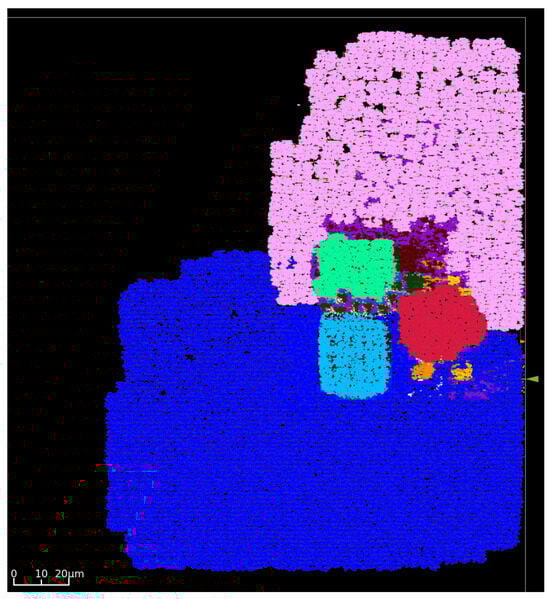
Figure 11.
Vector unit final placement using ASAP7 PDK.
- The multiplier, shown in navy blue, occupies the lower half of the layout and represents the largest component in terms of area.
- The adder, highlighted in cyan, is placed centrally within the multiplier block.
- The shifter unit appears to the right of the adder, marked in red.
- Bitwise logical and mask processing units are located above the adder and are highlighted in lime green.
- Surrounding the bitwise logic units is the Decode unit, shown in purple.
- The vector register file, marked in pink, is situated in the upper portion of the circuit.
4. Discussion
The implementation of the RISC-V Vector Extension enables the execution of vector operations, enhancing performance in a range of applications, such as Artificial Intelligence. However, supporting these operations typically requires additional hardware resources, which can increase circuit area and potentially reduce the maximum achievable operating frequency. The impact on area and performance depends heavily on the chosen microarchitecture; different design choices can favor either minimal area usage or maximum speed. While these two optimization goals are not strictly mutually exclusive, in practice, reducing area often comes at the cost of lower performance, and conversely, achieving higher frequency tends to require a larger silicon footprint.
While the proposed vector unit is fully functional and adheres to the RISC-V Vector Extension specification, several adaptations are still necessary to integrate it effectively into a high-performance core. One of the main limitations identified in the current implementation is the simplicity of its pipeline structure. Although a five-stage pipeline provides architectural clarity and ease of integration with academic cores, it imposes significant constraints on the maximum operating frequency, particularly in the Execute stage.
The Execute stage is a performance bottleneck, especially for operations that inherently require multiple cycles, such as division/multiplication. In its current form, the Execute stage handles a wide range of tasks, reading and decoding CSRs, performing the operation itself, and processing the result in a single stage. To improve performance and support higher clock frequencies, this stage can be decomposed into finer-grained substages.
A more advanced pipeline structure could divide the Execute stage into at least three distinct substages: (1) CSR decoding, where control and configuration registers are read and interpreted; (2) operation execution, which may require multiple cycles depending on the instruction complexity; and (3) result finalization, which includes result formatting, masking and ordering based on the vector configuration. By breaking down the execution logic into more manageable steps, the design can achieve better timing closure by reducing critical path delays.
Another area requiring close attention is the adder, which represents one of the most critical timing paths in the entire vector unit. Due to its high logic depth, it significantly limits the maximum achievable operating frequency. In the current implementation, 8-bit ripple carry adders are used throughout, which, while simple and area efficient, are suboptimal for high-speed designs due to the long carry propagation delays they introduce.
To address this limitation, several architectural improvements can be considered. First, the adder operation can be split into two separate pipeline stages. The first stage would handle only the arithmetic computation (addition or subtraction), while the second stage would process the condition flags (e.g., zero, sign, and carry) needed for comparison operations. This separation allows for a reduction in combinational logic per stage, easing timing closure and enabling higher clock speeds.
Additionally, the 8-bit adder architecture itself can be optimized by replacing ripple carry adders with faster alternatives, such as carry look-ahead or Kogge–Stone adders. These architectures significantly reduce carry propagation time, helping to mitigate one of the key timing bottlenecks in the design.
An alternative approach would be to introduce dedicated hardware units for normal vector operations and reduction operations. While this would effectively double the number of adder instances and increase the overall area, it would reduce the logic depth on each datapath, lower the overall gate capacitance, and minimize gate fanout, which is very important in digital circuit designs. Moreover, it would enable the parallel execution of element-wise and reduction operations, improving throughput and providing more flexibility for scheduling instructions in a high-performance core.
Another important factor to consider is the overall circuit area. A vector unit, depending on the maximum operand size it supports, can significantly increase the total area of the processor. This is primarily due to the wider datapaths and larger functional units required to handle high bit-width operations. A clear example of this is the multiplier: when configured to perform 128-bit multiplications, it occupies a substantial portion of the entire circuit area.
Therefore, careful architectural decisions must be made during the design of the vector unit. One of the key considerations is whether full-width operations must be executed entirely in parallel or if they can be decomposed into smaller, sequential operations. For instance, instead of performing a single 128-bit addition, the operation could be implemented as two 64-bit additions, where the carry from the lower half is propagated into the upper half. This strategy reduces datapath width and hardware complexity at the expense of some additional latency.
Similarly, a multi-cycle datapath can be considered as an alternative to a fully pipelined approach. A multi-cycle implementation reduces area by reusing functional units across cycles, but introduces constraints on instruction throughput. Specifically, consecutive operations that require the same hardware would need to wait for the resource to become available, decreasing the Instructions Per Cycle (IPC). However, if the target workloads use such wide or complex operations infrequently, this trade-off can be acceptable. In fact, it may yield substantial area savings without significantly impacting overall performance.
A third critical factor to consider is power consumption, which becomes increasingly significant as circuit complexity and logic density grow. When designing a vector unit with a wide range of functional blocks, it is essential to incorporate an effective power management strategy, such as clock gating or power gating, to disable unused components during operation.
For example, if the currently issued instruction is an addition, there is no need for the multiplier block to remain active. Even though its internal toggling does not affect the correctness of the operation, it results in unnecessary dynamic power consumption. Without appropriate gating, inactive units like the multiplier can contribute a considerable portion of the overall power draw, especially in deeply pipelined or high-frequency designs.
Finally, although not explored in detail in this work, an important avenue for future consideration is the integration of an out-of-order execution unit. Such an enhancement would allow the processor to issue and execute instructions based on operand availability rather than program order, effectively increasing instruction-level parallelism and boosting the overall Instructions Per Cycle (IPC) of the core.
5. Conclusions
This work presents a functional implementation of the RISC-V Vector Extension, focusing on a subset of arithmetic, logical, and permutation operations, with the aim of exploring vector execution in a simplified but modular environment. The implementation demonstrates compliance with the official specification and provides a platform suitable for academic exploration and potential integration with other cores based on RISC-V.
While the current design successfully supports basic vector operations, several challenges remain before it can be considered for high-performance applications. One of the main limitations is the use of a simplified five-stage pipeline, which restricts the maximum operating frequency, particularly due to the complexity of the Execute stage. Proposed improvements include decomposing this stage into finer substages and optimizing critical components such as the adder, which represents one of the longest logic paths.
In terms of area, the design choices such as operand widths and datapath configurations have a direct impact on circuit size. Techniques like operand slicing, multi-cycle execution, and functional unit sharing offer potential solutions to balance area and performance.
In relation to performance metrics, it is shown that the Vedic multiplier offers a clear advantage over array multipliers with lesser area and higher frequency operation for different configurations of bitwidth. Despite ASAP7, PDK is not manufacturable; it provides useful insight into possible performance results in commercial technology. It showed that in the overall design, a better nanometric technology offers better results.
As AI applications continue to expand into power-constrained and space-limited environments, alternative processing solutions beyond traditional GPUs become increasingly vital. Vector-enabled RISC-V CPU architectures offer a compelling and efficient path forward for embedded AI processing. By implementing a minimal yet robust set of vector instructions, this proposal validates the potential of lightweight Vector Engines to support essential AI operations with reduced overhead. This approach not only bridges part of the performance gap between CPUs and GPUs but also aligns with the industry’s growing emphasis on open-source, customizable, and energy-efficient hardware solutions for future AI workloads.
Finally, this contribution establishes a foundational vector execution unit and highlights the architectural and implementation trade-offs involved. It serves as a stepping stone for future research and optimization efforts.
Author Contributions
Investigation, M.B.-M.; writing—original draft preparation, M.B.-M.; writing—review and editing, L.P.-E. and O.L.-G.; supervision, L.P.-E. and O.L.-G. All authors have read and agreed to the published version of the manuscript.
Funding
This research received no external funding.
Data Availability Statement
The original contributions presented in this study are included in the article.
Conflicts of Interest
The authors declare no conflicts of interest.
Appendix A. Implemented Instructions
- The “RISC-V Vector Extension” can be accessed from RISC-V Technical Specifications (https://lf-riscv.atlassian.net/wiki/spaces/HOME/pages/16154899/RISC-V+Technical+Specifications+Archive, accessed on 29 April 2025).
Appendix A.1. Arithmetic Instructions
- VADD, VADC, VSUB, VSBC, VZEXT, VSEXT, VMUL, VMULH, VMULHU.
Appendix A.2. Logic Instructions
- VAND, VOR, VXOR, VSLL, VSRL, VSRA.
Appendix A.3. Compare Instructions
- VMSEQ, VMSNE, VMSLTU, VMSLT, VMSLEU, VMSLE, VMSGTU, VMSGT, VMINU, VMIN, VMAXU, VMAX.
Appendix A.4. Reduction Instructions
- VREDSUM, VREDMAXU, VREDMAX, VREDMINU, VREDMIN, VREDAND, VREDOR, VREDXOR.
Appendix A.5. Mask Instructions
- VMAND, VMNAND, VMANDN, VMXOR, VMOR, VMNOR, VMORN, VMXNOR.
Appendix A.6. Permutation Instructions
- VMV
Appendix B. Github Repository
- https://github.com/miguel100398/RISCV_V, accessed on 29 April 2025
References
- Iqbal, U.; Davies, T.; Perez, P. A Review of Recent Hardware and Software Advances. In GPU-Accelerated Edge-Computing Single-Board Computers (SBCs) for Computer Vision. Sensors 2024, 24, 4830. [Google Scholar] [CrossRef] [PubMed]
- Balasubramanian, K.K.; Salvo, M.D.; Rocchia, W.; Decherchi, S.; Crepaldi, M. Designing RISC-V Instruction Set Extensions for Artificial Neural Networks: An LLVM Compiler-Driven Perspective. IEEE Access 2024, 12, 55925–55944. [Google Scholar] [CrossRef]
- Kalapothas, S.; Galetakis, M.; Flamis, G.; Plessas, F.; Kitsos, P. A Survey on RISC-V-Based Machine Learning Ecosystem. Information 2023, 14, 64. [Google Scholar] [CrossRef]
- Johns, M.; Kazmierski, T.J. A Minimal RISC-V Vector Processor for Embedded Systems. In Proceedings of the 2020 Forum for Specification and Design Languages (FDL), Kiel, Germany, 15–17 September 2020. [Google Scholar] [CrossRef]
- Cavalcante, M.; Schuiki, F.; Zaruba, F.; Schaffner, M.; Benini, L. Ara: A 1-GHz+ Scalable and Energy-Efficient RISC-V Vector Processor With Multiprecision Floating-Point Support in 22-nm FD-SOI. IEEE Trans. Very Large Scale Integr. Syst. 2020, 28, 530–543. [Google Scholar] [CrossRef]
- Perotti, M.; Cavalcante, M.; Wistoff, N.; Andri, R.; Cavigelli, L.; Benini, L. A “New Ara” for Vector Computing: An Open Source Highly Efficient RISC-V V 1.0 Vector Processor Design. In Proceedings of the 2022 IEEE 33rd International Conference on Application-specific Systems, Architectures and Processors (ASAP), Gothenburg, Sweden, 12–14 July 2022. [Google Scholar] [CrossRef]
- Perotti, M.; Cavalcante, M.; Ottaviano, A.; Liu, J.; Benini, L. Yun: An Open-Source, 64-Bit RISC-V-Based Vector Processor With Multi-Precision Integer and Floating-Point Support in 65-nm CMOS. IEEE Trans. Circuits Syst. II Express Briefs 2023, 70, 3732–3736. [Google Scholar] [CrossRef]
- Wang, C.; Fang, C.; Wu, X.; Wang, Z.; Lin, J. SPEED: A Scalable RISC-V Vector Processor Enabling Efficient Multiprecision DNN Inference. IEEE Trans. Very Large Scale Integr. Syst. 2025, 33, 207–220. [Google Scholar] [CrossRef]
- Lee, J.K.L.; Jamieson, M.; Jesus, R. Test-Driving RISC-V Vector Hardware for HPC. In Proceedings of the International Conference on High Performance Computing, Hamburg, Germany, 21–25 May 2023. [Google Scholar] [CrossRef]
- Dakić, V.; Mršić, L.; Kunić, Z.; Đambić, G. Evaluating ARM and RISC-V Architectures for High-Performance Computing with Docker and Kubernetes. Electronics 2024, 13, 3494. [Google Scholar] [CrossRef]
- Sordillo, S.; Cheikh, A.; Mastrandrea, A.; Menichelli, F.; Olivieri, M. Customizable Vector Acceleration. In Extreme-Edge Computing: A RISC-V Software/Hardware Architecture Study on VGG-16 Implementation. Electronics 2021, 10, 518. [Google Scholar] [CrossRef]
- Patsidis, K.; Nicopoulos, C.; Sirakoulis, G.C.; Dimitrakopoulos, G. RISC-V2: A Scalable RISC-V Vector Processor. In Proceedings of the 2020 IEEE International Symposium on Circuits and Systems (ISCAS), Seville, Spain, 12–14 October 2020; pp. 1–5. [Google Scholar] [CrossRef]
- Oh, H.W.; Lee, S.E. The Design of Optimized RISC Processor for Edge Artificial Intelligence Based on Custom Instruction Set Extension. IEEE Access 2023, 11, 49409–49421. [Google Scholar] [CrossRef]
- Allen, T.; Ge, R. Demystifying GPU UVM Cost with Deep Runtime and Workload Analysis. In Proceedings of the IEEE International Parallel and Distributed Processing Symposium (IPDPS), Portland, OR, USA, 17–21 May 2021; pp. 141–150. [Google Scholar] [CrossRef]
- RISC-V V Vector Extension. Rev. 1.0. Available online: https://riscv.org/specifications/ratified/ (accessed on 7 March 2024).
- Kahar, D.K.; Mehta, H. High-speed Vedic multiplier used Vedic mathematics. In Proceedings of the 2017 International Conference on Intelligent Computing and Control Systems (ICICCS), Madurai, India, 15–16 June 2017; pp. 356–359. [Google Scholar]
- Ajayi, T.; Chhabria, V.A.; Fogaça, M.; Hashemi, S.; Hosny, A.; Kahng, A.B.; Kim, M.; Lee, J.; Mallappa, U.; Neseem, M.; et al. Toward an open-source digital flow: First learnings from the openroad project. In Proceedings of the 56th Annual Design Automation Conference 2019, Las Vegas, NV, USA, 2–6 June 2019; pp. 1–4. [Google Scholar]
- gf180mcu-pdk. Available online: https://github.com/google/gf180mcu-pdk (accessed on 29 April 2025).
- skywater-pdk. Available online: https://github.com/google/skywater-pdk (accessed on 29 April 2025).
- FreePDK45. Available online: https://eda.ncsu.edu/freepdk/freepdk45 (accessed on 29 April 2025).
- Lawrence, T. Clark and Vinay Vashishtha and Lucian Shifren and Aditya Gujja and Saurabh Sinha and Brian Cline and Chandarasekaran Ramamurthy and Greg Yeric. ASAP7: A 7-nm finFET predictive process design kit. Microelectron. J. 2016, 53, 105–115. [Google Scholar]


Disclaimer/Publisher’s Note: The statements, opinions and data contained in all publications are solely those of the individual author(s) and contributor(s) and not of MDPI and/or the editor(s). MDPI and/or the editor(s) disclaim responsibility for any injury to people or property resulting from any ideas, methods, instructions or products referred to in the content. |
© 2025 by the authors. Licensee MDPI, Basel, Switzerland. This article is an open access article distributed under the terms and conditions of the Creative Commons Attribution (CC BY) license (https://creativecommons.org/licenses/by/4.0/).