Abstract
This paper presents a novel fully integrated radio frequency (RF) rectifier tailored for a wide power dynamic range (PDR) with multiband adaptability to efficiently convert AC RF power into DC power. The proposed rectifier utilizes the strength of interstage gate biasing to achieve high power conversion efficiency (PCE) across a broad range of input power levels. Through its reconfigurable mode, the circuit seamlessly transitions between a low-power path and high-power path to ensure optimal performance across a wide PDR. Simulated using CMOS 65 nm technology, the post-layout assessment reveals a peak PCE of 48.8% at 900 MHz and 46.4% at 1800 MHz, with an extensive PDR of 20 dB for PCE exceeding 20% at both frequencies.
1. Introduction
The Fourth Industrial Revolution (IR 4.0) has catalyzed advancements in IoT systems, pushing a greater demand for energy-efficient, low-power devices that can operate autonomously over extended periods [1]. In IoT and wireless sensor networks (WSN), low-power nodes are increasingly being deployed in remote locations or hard-to-reach environments, where the traditional battery-powered solutions are not viable due to maintenance and replacement challenges. This has led to the development of innovative technologies, like radio frequency energy harvesting (RFEH), which enables battery assist to these low-power devices, effectively extending their operational lifetimes or reducing the dependency on conventional power sources [2,3]. The flexibility of RFEH systems allows IoT devices to be deployed in diverse applications, such as biomedical sensors, wearables, and consumer electronics. Hence, it requires features, like a wide input power range and multiband adaptability, to ensure reliable energy harvesting and power conversion in dynamic and unpredictable conditions.
In radio frequency energy harvesting (RFEH) systems, the ability to operate efficiently across a wide input power range is crucial due to the variable nature of ambient RF energy sources. In fact, recent studies [4,5,6,7] have extensively explored the potential of RFEH systems operating in the microwatt power range, which is critical for enabling self-powered devices in applications. These works demonstrate that even under ultra-low input power conditions, efficient rectifier design and energy management techniques can make RFEH a viable solution for long-term autonomous operation without battery replacement. Ambient RF power levels can fluctuate significantly based on factors, such as distance from the source, environmental conditions, and the presence of obstacles [7]. A wide input power dynamic range (PDR) in RFEH systems also has direct impact on low-power devices. Since energy availability fluctuates based on RF conditions, a system that can operate over a broad power range allows devices to remain functional even when RF power levels momentarily drop. This is particularly useful for IoT sensors and wireless sensor networks, where stable operation of the RFEH system across different locations is essential for mobility and adaptability [8].
Multiband adaptability is a crucial feature in RF energy harvesting (RFEH) rectifier design, as ambient RF signals are inherently distributed across multiple frequency bands, creating a dynamic and unpredictable energy environment. A single-band rectifier has restricted performance in such dynamic environments as it becomes inefficient when the rectifier target frequency is unavailable, experiences fluctuations, or has low-power density. In contrast, a multiband rectifier [8,9,10] can capture and combine energy from various frequency sources—such as GSM (900 MHz, 1800 MHz), Wi-Fi (2.4 GHz, 5 GHz), and 4G/5G networks [6]—maximizing harvested power and ensuring consistent operation. This adaptability is particularly important in real-world scenarios where signal strength varies due to environmental factors, user density, and RF consumption patterns. For instance, in urban areas, 900 MHz and 1800 MHz bands are often highly saturated [11] due to widespread mobile communication usage, making them ideal reference frequencies for multiband rectifier design. By supporting multiple frequency bands, RFEH systems can maintain optimal power conversion efficiency (PCE) across diverse conditions, enhancing reliability for IoT devices, wireless sensor networks, and other low-power applications when energy availability is sporadic [10].
On-chip integration enhances circuit compactness, minimizes parasitic effects, and improves overall system efficiency by eliminating the need for external components [12]. This approach is particularly beneficial for miniaturized and low-power applications, such as biomedical implants and IoT devices, where space and power efficiency are critical. A fully integrated CMOS rectifier can be realized using CMOS technology, enabling efficient RF-to-DC conversion while maintaining a small footprint, PCE, and extended PDR [13].
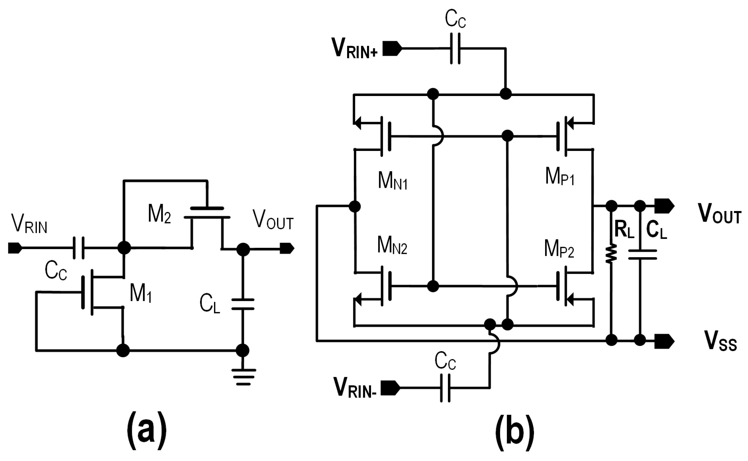
There are many types of CMOS rectifier configurations in the RFEH system. The commonly used configurations are Dickson and cross-coupled differential drive (CCDD) rectifiers, as shown in Figure 1a and Figure 1b, respectively. Due to the voltage drop of diode configuration, Dickson rectifier suffers from poor sensitivity at low RF input power, which will affect the overall performance for low-power devices [14]. CCDD was first introduced by [15], reporting good energy conversion efficiency PCE up to 67.5% at 953 MHz. Unlike single-ended topology, like the Dickson rectifier, the differential configuration is evaluated to be more effective as it eliminates the diode voltage and uses the CMOS transistors as switches, giving low ON-resistance in forward bias, thus improving the sensitivity. Therefore, CCDD topology has a relatively high PCE in low-power regions but suffers from dropped efficiency in high-power regions due to leakage currents.

Figure 1.
Commonly used CMOS rectifier topologies: (a) Dickson, (b) CCDD.
Prior rectifier designs employed body-biasing techniques by modulating the bulk voltage to decrease the threshold voltage of CMOS transistors in conventional CCDD to improve sensitivity [16]. However, this approach is constrained by the maximum Vsb, leading to very narrow PDR at 8 dB [17,18]. While [19] achieves a high sensitivity of −38 dBm using feedback self-adaptive body biasing, its performance is degraded significantly at high input power levels, limiting its practical applicability.
Other than body biasing, gate biasing is another considerable way to improve the performance of CCDD rectifiers. Referring to the CCDD rectifier architecture in Figure 1b, CMOS transistors’ source terminal is tied to the RF input (RF+/RF−), and the drain is connected to the output (Vout). Hence, gate biasing is the most suitable approach as it can be independently controlled without interfering with RF signals or the DC output, whereas biasing the source or drain is impractical as it would disrupt the RF input signal or introduce unwanted loading effects on the output. The self-gate biasing mechanism is introduced to dynamically adjust VGS, enhancing conduction during positive rectification. Key methods include using feedback resistors [20,21], diodes [22], diode-connected MOSFETs [23,24,25,26], and non-linear self-gate biasing [27], which suppress reverse leakage current at high output power, thereby extending PDR to the high power side. Interstage gate-biasing is also employed by [28,29] to enhance conduction at low RF amplitudes, but the biasing voltage increases proportionally with the number of rectifying stages that results in large VGS swings on the high power side, leaving narrow PDR at a low input power level. Another gate-biasing technique is the bootstrapping circuit [30,31], which employs capacitors to store and transfer a more negative bias voltage to the gates of PMOS rectifying transistors, enabling high power conversion efficiency (PCE) at low input power levels. Ref. [31] advanced this prior design by incorporating a bootstrapping clamper with the dynamic threshold reduction (DTR) technique, thereby extending high PCE operation from 60 MHz in [30] up to 402 MHz and 953 MHz, showing multiband adaptability. However, a key limitation is their narrow power dynamic range (PDR), making them less suitable for ambient energy harvesting applications where input power can vary significantly. In this work, the proposed design introduces reconfigurable operation modes by employing the interstage gate-biasing technique, which can dynamically switch between low-power and high-power paths to maintain optimal efficiency across a wide PDR. This adaptability ensures robust performance in real-world scenarios with fluctuating RF energy availability.
The purpose of this work is to improve the PDR of the CMOS rectifier to be suitable for a multiband environment with dynamic input power. To enhance PDR, a few studies propose reconfigurable mode rectifiers, such as stage variation, dual-path, and hybrid topologies. Stage variation rectifiers [32,33,34,35] dynamically configure the number of active rectifier stages to boost the DC voltage in low-power mode and minimize conduction loss in high-power mode. Dual-path rectifiers [36,37] integrate low-power and high-power rectification paths into a system to maximize the PCE at both regions. Three-mode reconfigurable rectifiers [38] employ stacked CCDD architectures, dynamically modulating transistors’ length to suppress the leakage current across low-, medium-, and high-power zones, further extending the PDR. It is observed that most of the reconfigurable rectifiers primarily focus on optimizing the high-power zone by reducing conduction loss or mitigating leakage. This approach inherently limits the power conversion efficiency (PCE) at low input power due to the minimum sensitivity threshold of the CCDD architecture, where the rectifier fails to efficiently convert RF energy below a certain input power level. However, due to the structural constraints of CCDD, there are no significant architectural modifications to enhance performance at low power levels. As a result, the PDR extension remains limited on the low-power side, restricting their effectiveness in ambient energy harvesting environments where ultra-low power operation is essential for reliable energy conversion.
This paper proposes an enhanced fully integrated reconfigurable rectifier, using dual-mode single-path interstage gate-biasing technique to extend the high PCE range (or PDR) at both low and high input power. Section 2 explains the working principle of the proposed work and the realization of the circuit. Section 3 presents the experimental results. Lastly, a conclusion is drawn in Section 4.
2. Proposed Work
2.1. Background
Figure 2 illustrates how CCDD rectifiers suffer from current leakage at high RF input power, limiting their PDR. This occurs when the PMOS has sufficient VSG to turn on the transistors while the output voltage exceeds the RF signal amplitude, causing current reverse flow from the output back to RF input, through the PMOS. To address this issue, gate biasing on the PMOS is introduced as an optimal solution to extend PDR, as it provides better control over the transistor’s conduction characteristics. In the CCDD architecture, the drain-to-source current (IDS) follows Equation (1) when it is in saturation region, where the gate-to-source source voltage (VGS for NMOS or VSG for PMOS) plays a crucial role in determining conduction behavior.
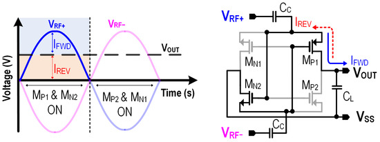
Figure 2.
Illustration of reverse leakage current on CCDD rectifiers when VOUT > VRF.
At low RF power, a large VSG for PMOS is required to lower the effective threshold voltage (VTH), ensuring strong conduction despite the weak RF input. Conversely, at high RF power, excessive VSG swings can lead to reverse conduction, where transistors turn ON while the output terminal has higher potential, causing reverse leakage current which reduces efficiency. By dynamically adjusting VGS or VSG based on input power, gate biasing enhances conduction at low power and suppresses leakage at high power, significantly extending the PDR. As mentioned in the introduction, source or drain biasing lacks adaptability, gate biasing offers precise control over conduction characteristics, making it the most effective approach for improving PCE and overall rectifier performance in CCDD.
The gate-biasing technique can affect the ON resistance of the CMOS transistors, as given by Equation (2):
where: μn is the carrier mobility, COX is the gate oxide capacitance, W/L is the transistor ratio, VGS is the gate-to-source voltage, VTH is the threshold voltage. By increasing VGS − VTH, RON could be lowered and thus less RF input power is required to turn on the transistors. At low input power, this technique ensures VGS − VTH remains sufficient for conduction, improving rectifier sensitivity. However, at high input power, a high gate-biased voltage will cause larger VGS − VTH swings which will lead to exponential growth in reverse leakage current, as described by Equation (3):
where: Vt is the thermal voltage and VDS is the drain-to-source voltage. Thus, gate-biasing requires adaptive bias control to increase/decrease the gate voltage applied to the PMOS transistors to improve sensitivity at low power and mitigate the reverse leakage current at high power.
In this work, a novel interstage gate-biasing technique is used to regulate the gate voltage, VG of PMOS transistors in the rectifier circuit by using the signals from different rectifier stages. This paper will present a dual-mode single-path reconfigurable rectifier that integrates preceding and succeeding interstage gate-biasing configuration within a single rectification path to ensure wide PDR across low and high input power. Detailed circuit architecture and working principles are described in Section 2.2.
2.2. Architecture and Working Principle
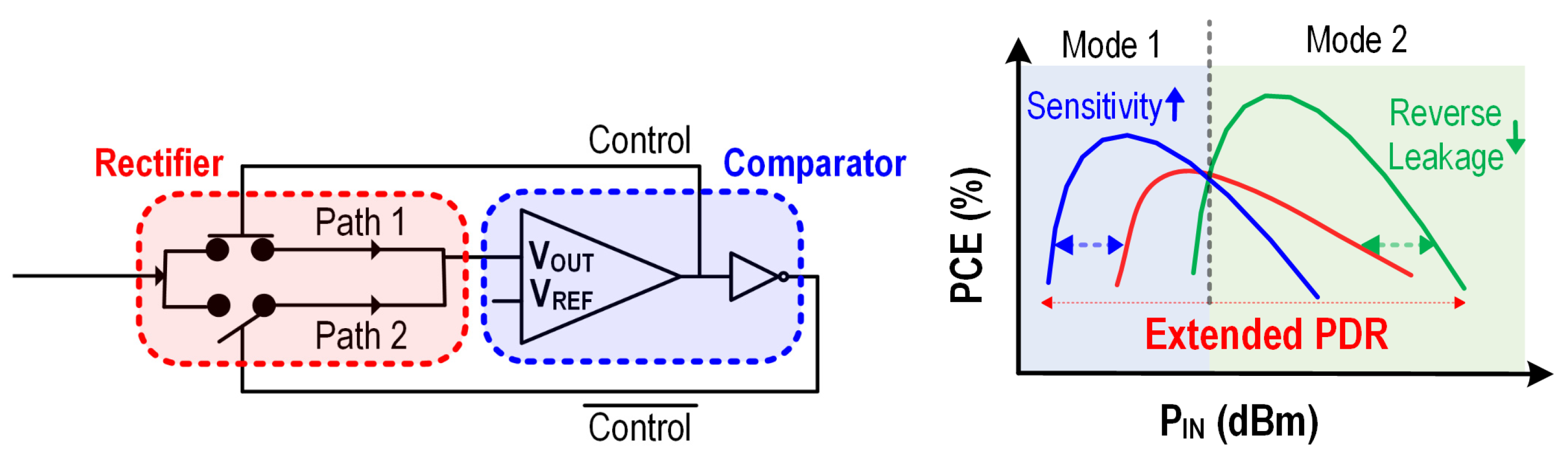
Figure 3 shows the conceptual design architecture of the proposed dual-mode single-path reconfigurable fully integrated rectifier, which consists of a main novel rectifier for RF-DC conversion, and a comparator circuit to compare between low and high input power for adaptive switching control. The idea is to compare a target output voltage with a switching point voltage. If the target output voltage is lower than the switching point voltage, the input power is considered low, prompting the rectifier circuit to use Path 1 for rectification. Conversely, if the target voltage exceeds the switching point voltage, the circuit will use Path 2 for rectification. Building on this understanding, the proposed rectifier operates in two distinct modes: Mode 1 engages the preceding stage configuration at low input power, while Mode 2 activates succeeding stage at high input power. This approach effectively addresses both the capped sensitivity and reverse leakage issues in the CCDD rectifier.
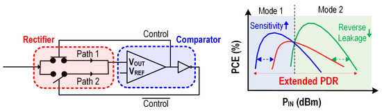
Figure 3.
Design framework for the proposed dual-mode single path reconfigurable rectifier design with an adaptive control for mode switching to achieve wide PDR.
At the preceding stage, PMOS transistors are biased by the VG of previous rectifier stage while the source VS is still tied to the current rectifier stage. Since the VG at the previous rectifier stage is low, VSG at the current stage becomes relatively high that makes PMOS transistors easier to turn on, thereby improving the sensitivity. When the rectifier switches to the succeeding stage, PMOS transistors will be biased by the VG of the next rectifier stage while VS remains at the current rectifier stage, similar to the preceding biasing approach. The VG at the next rectifier stage is higher, which will lower the VSG and prevent the reverse leakage of PMOS transistors.
Preceding interstage gate-biasing can enhance the sensitivity of CCDD by providing a lower VG from the previous rectifier stage, giving higher VSG for better forward conduction at low input power. However, this alone does not effectively suppress the leakage current at a high input power because static gate biasing increases, causing larger VGS − VTH swings in the end, which lead to exponential growth in the reverse leakage current. Hence, succeeding interstage gate-biasing topology is used at a high input power to reduce the VGS voltage swing, keeping transistors in the optimal conduction region.
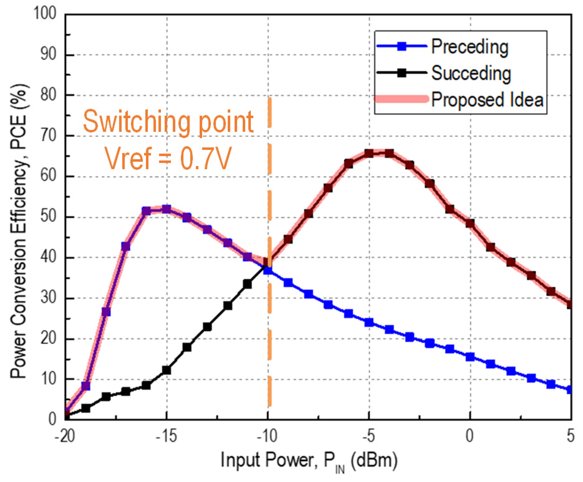
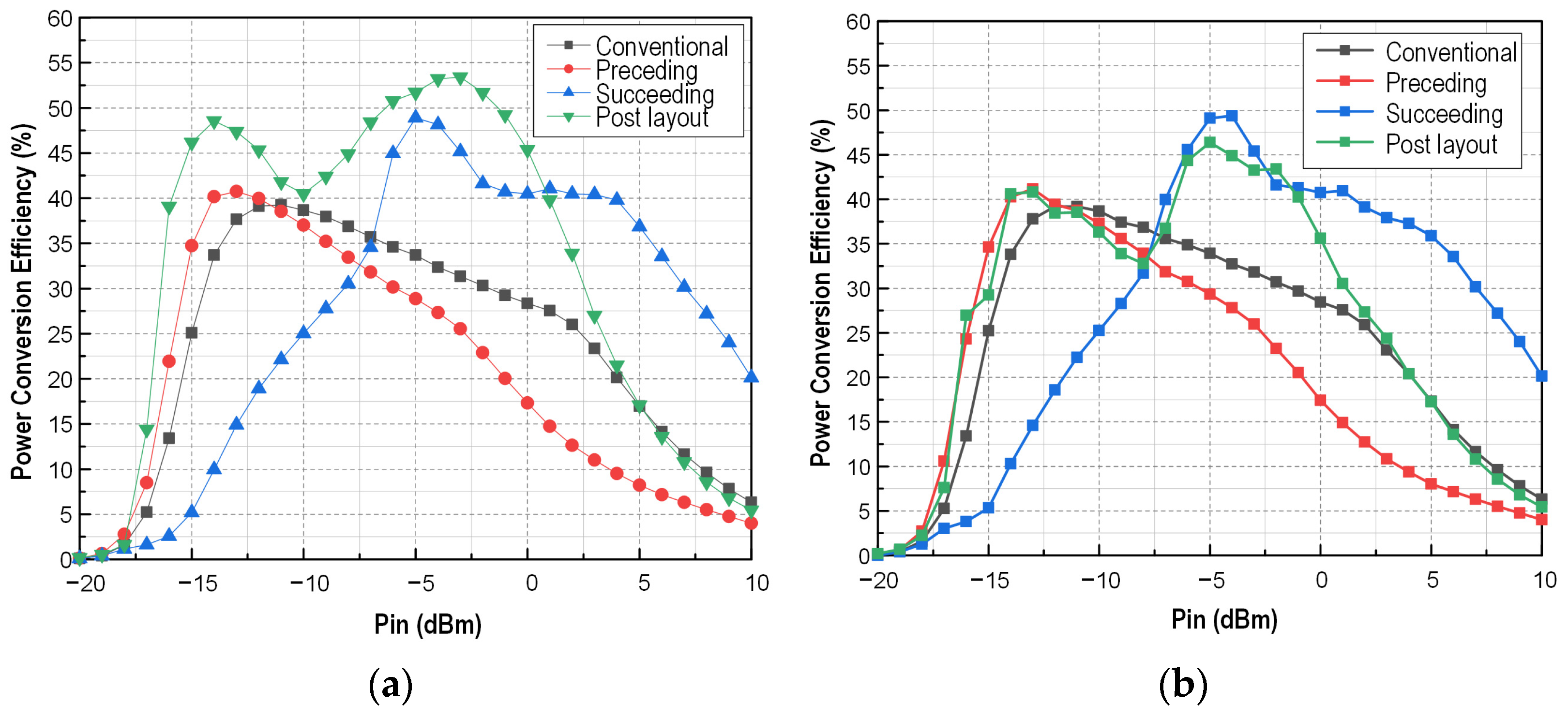
The simulation result in Figure 4 shows that preceding and succeeding interstage gate biasing appears as a promising configuration for low and high input power rectification, respectively.
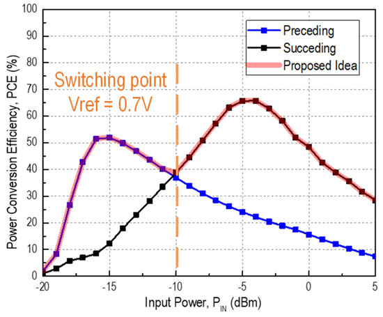
Figure 4.
Simulated PCE graph from preceding and succeeding interstage gate biasing.
From Figure 4, it is observed that a narrow PDR could be obtained from either one of the gate-biasing topologies. Reconfigurable mode rectifier is proposed to combine both graphs to extend the PDR. An additional comparator circuit is introduced, making it more complex but significantly more efficient and adaptable to wide input power level. The switching point between 2 modes can also be determined from the PCE graph above, where preceding interstage gate-biasing configuration achieves wide PDR when the target output voltage is lower than 0.7 V while the succeeding interstage gate-biasing configuration is has better performance at the target output voltage higher than 0.7 V. Hence, Vref = 0.7 is selected as the switching point voltage. This mechanism ensures that the rectifier dynamically reconfigures itself to operate in the mode that provides higher efficiency, depending on the input power and load conditions.
This innovative approach addresses the limitations of the base model, making it suitable for applications requiring wide PDR and reliable rectification performance. Besides, the proposed dual-mode single-path rectifier architecture also eliminates the need for parallel rectifier architectures, which would otherwise increase chip size and power consumption. By integrating multiple configurations into a single design using simple wiring, the design complexity can be minimized, thereby preventing degradation of the rectifier’s overall efficiency.
2.3. Realization of Circuit
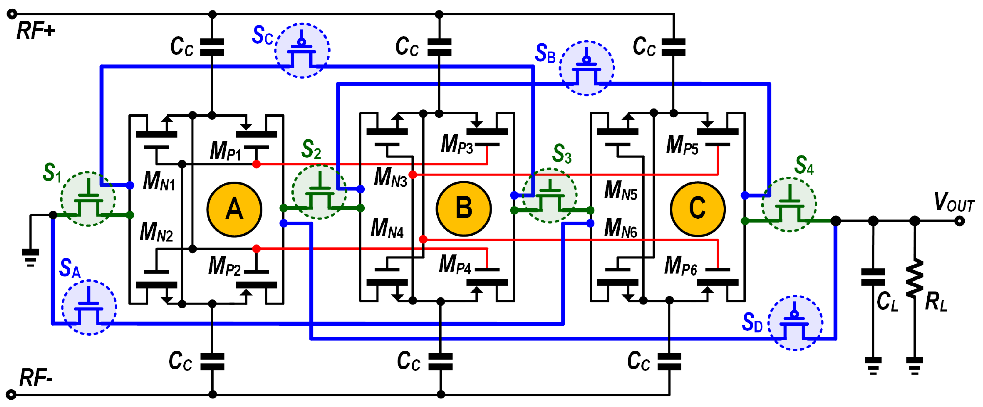
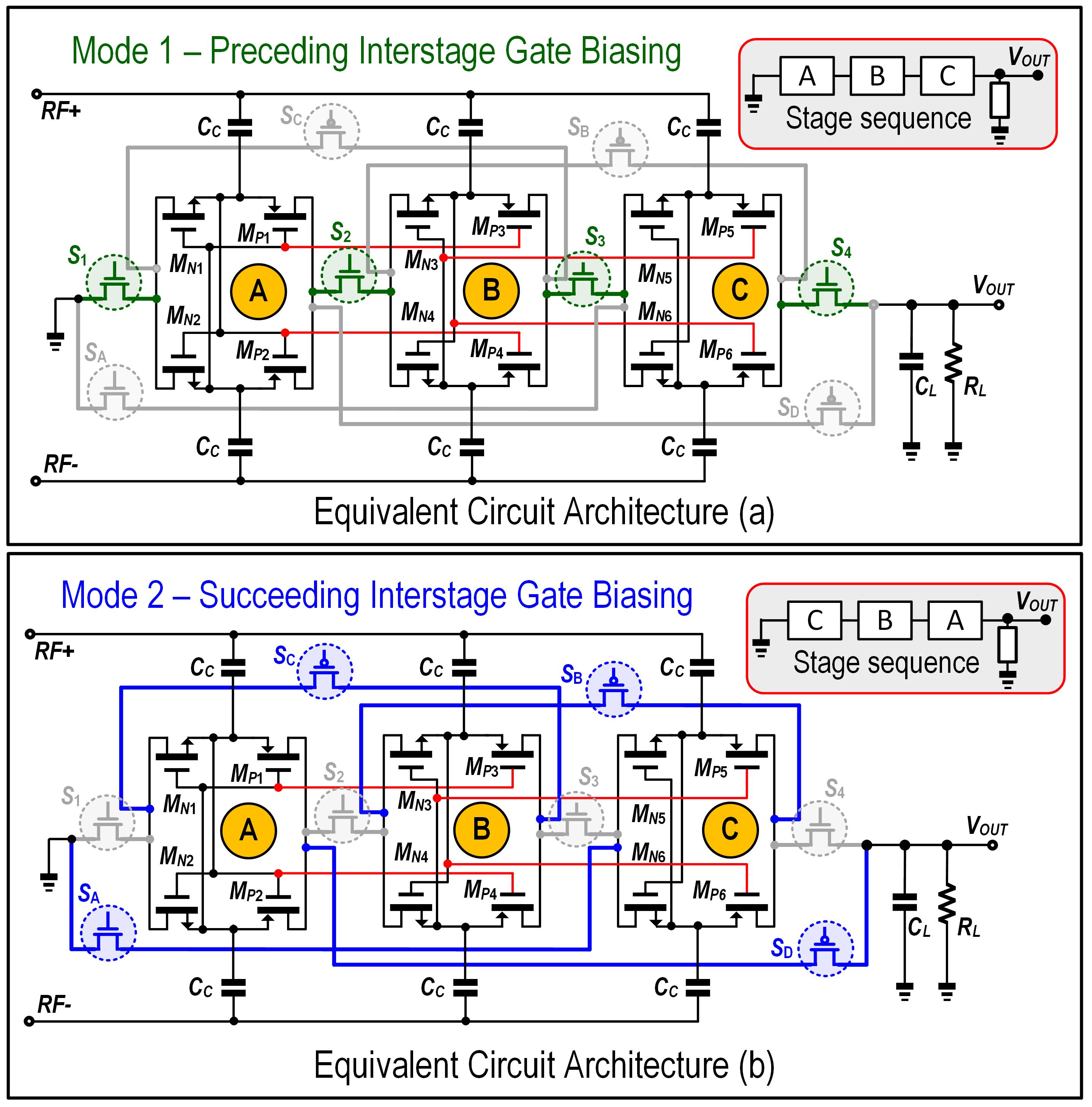
In TSMC 65 nm CMOS process, low-threshold-voltage transistors (LVT) are chosen to optimize the rectifier’s PCE as it requires smaller gate-to-source voltage (VGS) to turn on. The NMOS has the width of 1 µm while the PMOS widths are 2 µm with both having the same channel length of 60 nm. The same transistor sizing is used for both the rectifier and comparator blocks. Figure 5 shows the three-stage rectifier that integrates both preceding and succeeding circuit architecture. The circuit consists of three stages labelled as Stage A, Stage B, and Stage C. The switches in between every cascaded stage (S1, S2, S3, S4 for Mode 1 and SA, SB, SC, SD for Mode 2) are MOSFET switches, which will be controlled by the comparator logic circuit, as shown in Figure 6. For easier understanding, the circuit schematic in Figure 5 has been restructured in Figure 7 to illustrate the circuit architecture during low power (Mode 1) and high power (Mode 2).
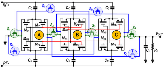
Figure 5.
Schematic of the 3-stage dual-mode single-path reconfigurable interstage rectifier.
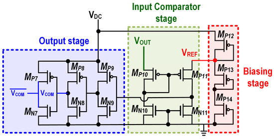
Figure 6.
Schematic of comparator circuit.
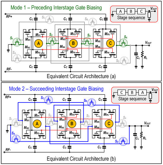
Figure 7.
Equivalent circuit during (a) Mode 1 (for low power) and (b) Mode 2 (for high power).
At low input power, the circuit operates in Mode 1, where green switches (S1, S2, S3, S4) are turned on, while Path 2 (blue switches) remains off, ensuring that current flows only through the active switches. In this configuration, the rectifier follows a preceding interstage connection (A → B → C). Initially, Stage A begins the rectification process, followed by Stage B and Stage C, which progressively boost the rectified voltage using the stored charge from the previous stage. Stage C completes the rectification, generating a higher DC voltage for low-power energy harvesting applications. In this mode, the PMOS transistors are gate-biased with a higher VSG, reducing ON-resistance and enhancing forward conduction, thereby improving rectifier sensitivity.
At high input power, Mode 2 is activated as switches SA, SB, SC, and SD turn on, transitioning the circuit into a succeeding interstage configuration (C → B → A). Here, the rectification sequence is reversed, with Stage C handling the initial rectification step at high power levels using stored charge from the next rectifier stage. This prevents the early stages from overcharging and leaking current back to the RF input, effectively extending the PDR to the low-power region while maintaining efficiency at high power. Since higher input power naturally enables transistor conduction, reverse leakage current increases compared to Mode 1. To mitigate this, the rectifying PMOS transistors are biased with a lower VSG, effectively reducing leakage current and ensuring stable operation at high input power levels.
Referring to Figure 6, the comparator circuit functions as a switch controller because its output will generate two main control signals, Vcom and to activate or deactivate the 8 MOSFET switching elements, S1 to S4 and SA to SD. CMOS Op-Amp is used to compare the rectifier output voltage, Vout with the reference voltage, Vref of 0.7 V. This reference voltage is generated using a voltage divider circuit, ensuring a stable and consistent bias point for accurate comparison. At the output stage, an inverter is added to the comparator output; this can allow two complementary switching controls to happen simultaneously. Vcom and will change based on the comparison of Vout with Vref to determine which set of switches (Mode 1 or Mode 2) is active. The detailed control states for each mode are summarized in Table 1.

Table 1.
Control signal logic for mode switching.
In this design, we utilize the TSMC 65 nm low-power (LP) CMOS process, where the threshold voltages, VTH of LVT NMOS and PMOS transistors are approximately 400–500 mV. To ensure reliable switching, a VDC = 1.2 V supply is selected to power the comparator, allowing the control signals to swing between 0 V and 1.2 V. During Mode 1 operation, for example, switch S4 must be remained “ON” before Vout reaches a switching point voltage of 0.7 V. At this point, the control signal corresponding to S4 is VCOM = 1.2 V; therefore, a sufficient VGS swing is still sufficient to turn on the switch when the source voltage, Vs of the switch S4 lies within the 0–0.7 V range.
3. Experimental Results
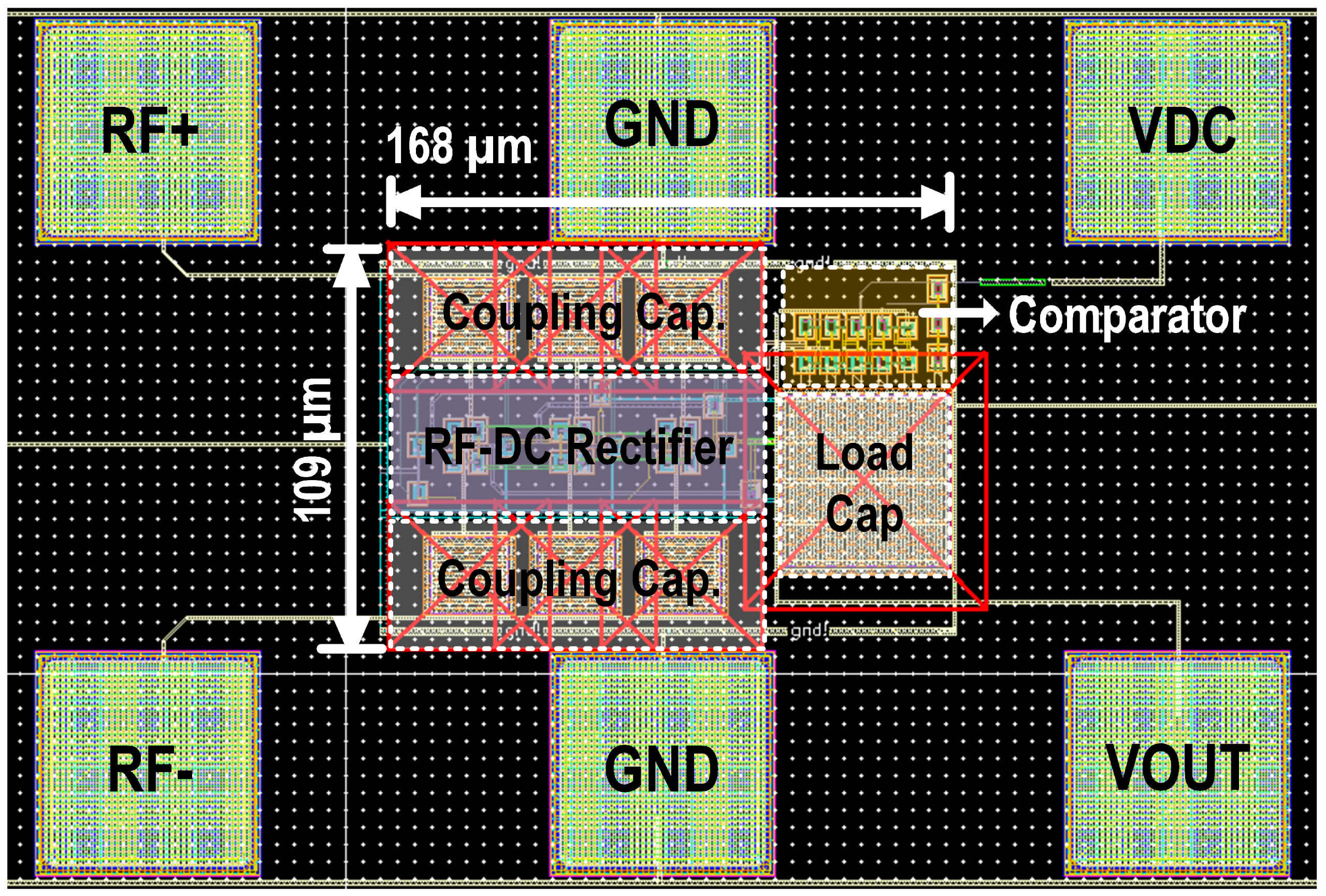
The proposed design is implemented using 65 nm CMOS node, which occupies an effective chip area of 0.0183 mm2, excluding the bond pad. Figure 8 shows the overall layout of the fully integrated on-chip rectifier design. In the post layout simulation, the same transistor sizing was used for both 900 MHz and 1.8 GHz operations. The detailed transistor and other device parameters are tabulated in Table 2.
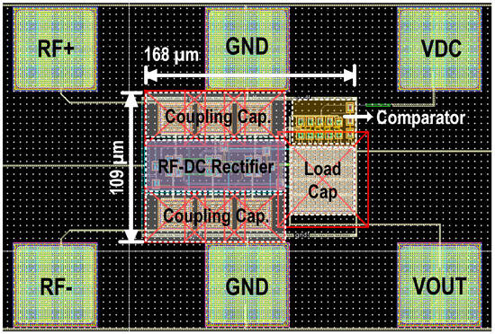
Figure 8.
Layout of the proposed rectifier design.
Table 2.
Transistor sizing table.
The input power fed into the rectifier is determined by using the equation below:
PR is the input RF incident power received from the antenna and is the power reflection coefficient. Taking the output from the comparator as Pout, the PCE of the rectifier can be calculated by:
Conducting post-layout simulations under 900 MHz and 1.8 GHz with 100 kΩ load resistor and 5 pF load capacitor, the simulated graphs of PCE versus Pin of the proposed design are shown in the Figure 9a,b. The performance result at both operating frequencies was compared respectively with a conventional cross-coupled differential drive (CCDD) rectifier and which uses with the same design parameters. In post-layout simulation, the proposed idea achieved PDR of 20 dB with peak PCE of 48.6% at −13.48 dBm in Mode 1 while peak PCE achieves 53.4% at −3.48 dBm in Mode 2 at a 900 MHz operating frequency.
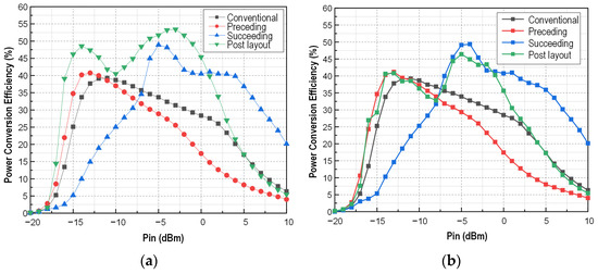
Figure 9.
Post layout simulation graph of PCE in (a) 900 MHz and (b) 1.8 GHz.
At a 1.8 GHz operating frequency, there is a drop in PCE across the range of input power, giving 41.4% at −13 dBm in Mode 1, while peak PCE achieves 46.4% peak PCE at −5 dBm in Mode 2. However, the PDR still can be maintained at 20 dB, which is consistent despite varying ambient RF conditions. Figure 9 compares the proposed rectifier with the conventional CCDD [15], operating at 900 MHz and 1.8 GHz, respectively. The proposed dual-mode single-path gate-biasing technique successfully improved the PCE in a low-power region, achieving wider PDR compared to the conventional CCDD.
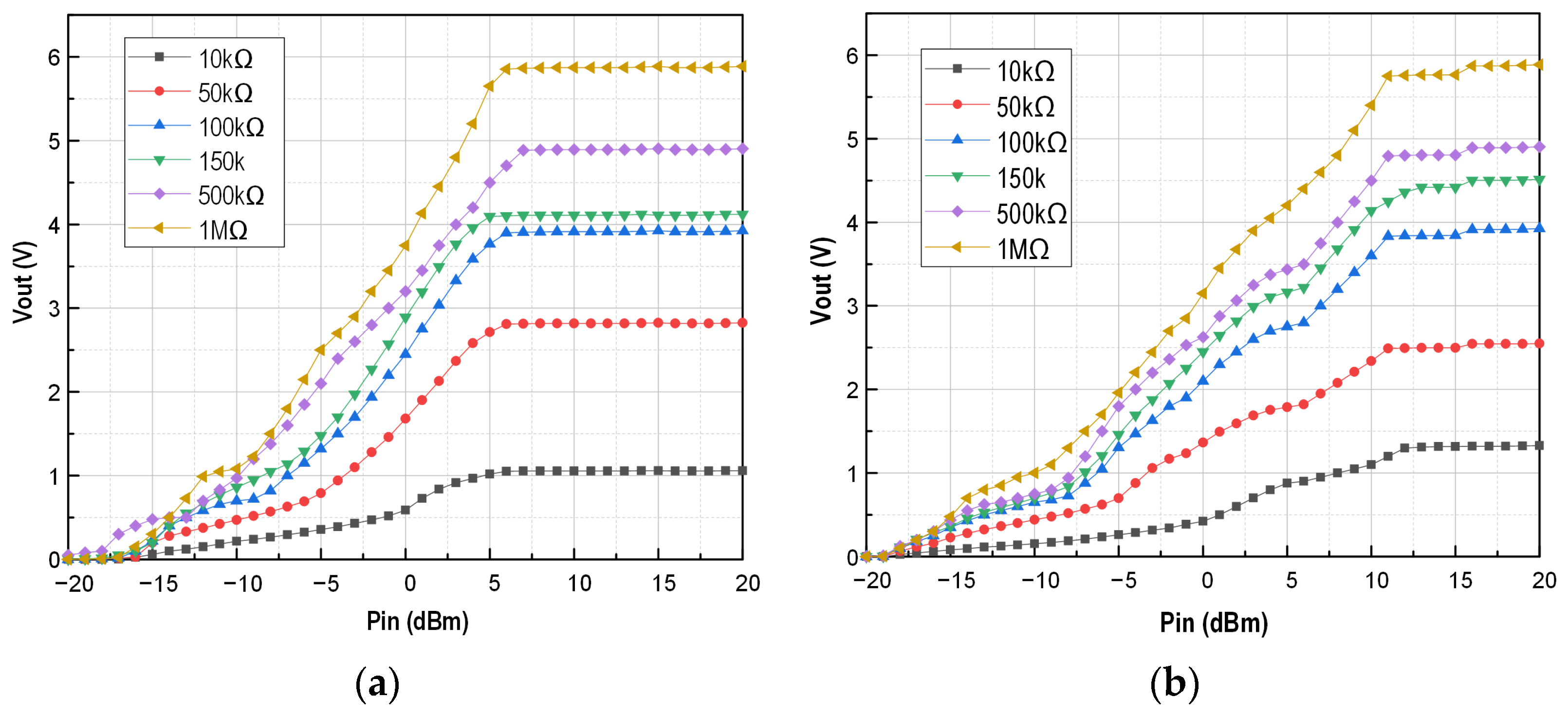
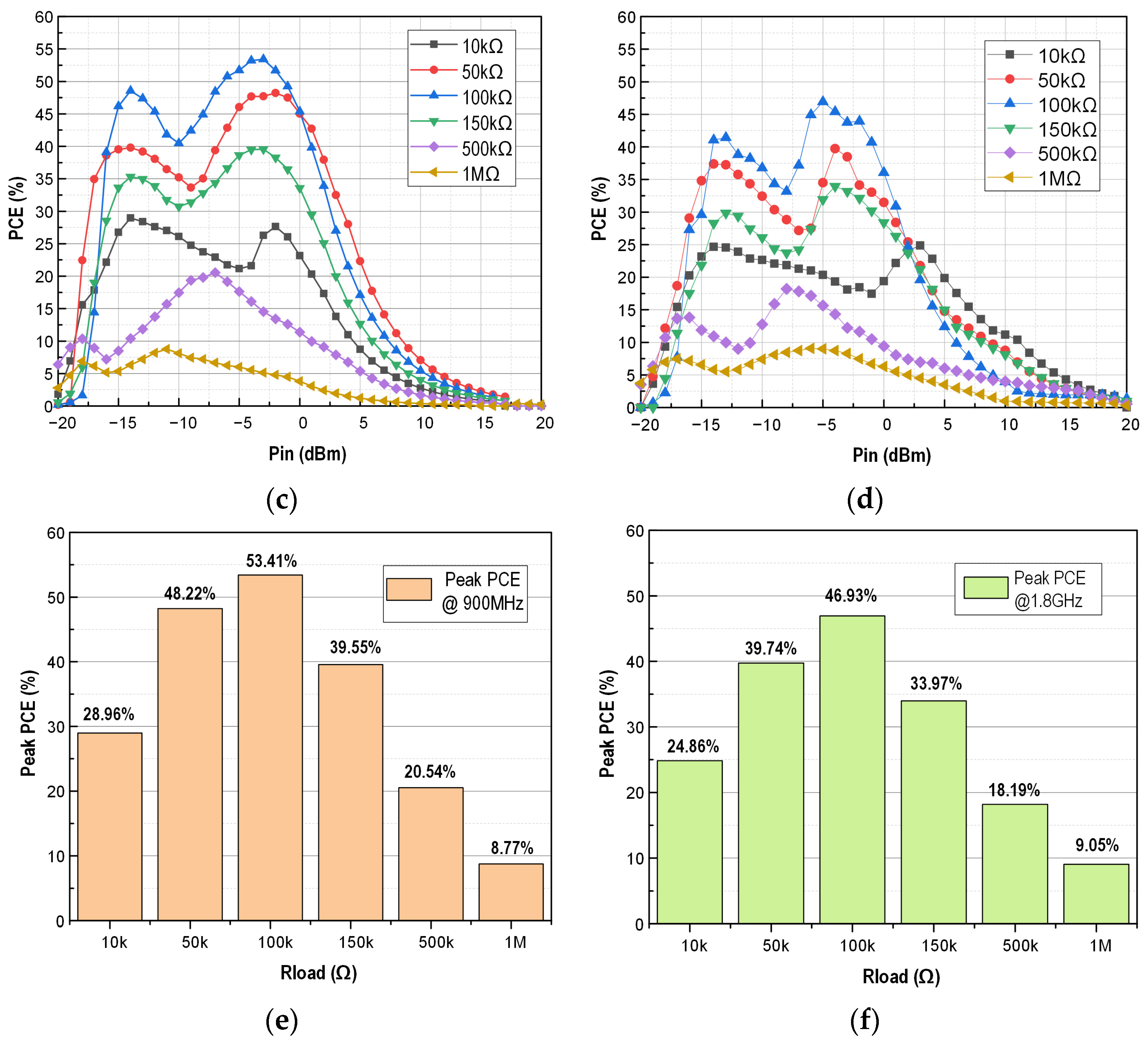
Besides, additional analyses were performed to evaluate the rectifier’s robustness under varying load conditions. Based on simulation analysis, the optimal load range falls between 10 kΩ and 150 kΩ as the proposed rectifier exhibits a higher PCE, more than 20%, and achieve PDR around 20 dB. A value of 100 kΩ was selected for our primary analysis as it lies within this optimized region and is commonly adopted in CMOS rectifier designs [14,15,39,40] for performance benchmarking. The performance of the proposed rectifier at 900 MHz and 1.8 GHz under various loads is shown in Figure 10 below.
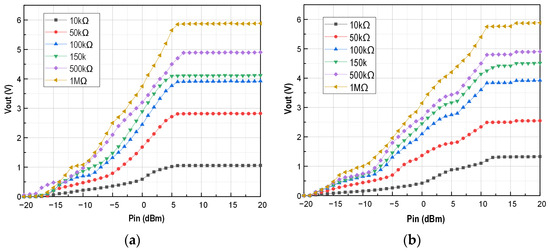
Figure 10.
Performance graphs of the proposed rectifier under various loads. Simulated Vout against Pin in (a) 900 MHz and (b)1.8 GHz. Graphs of PCE against Pin in (c) 900 MHz and (d) 1.8 GHz. Peak PCE performance at (e) 900 MHz and (f) 1.8 GHz.
Table 3 presents a comprehensive summary of rectifier’s performance and comparison with previous state-of-the-art designs. Although the proposed rectifier does not achieve the highest peak PCE among the compared works, it outperforms others by offering the widest PDR, which is 20 dB. This extended PDR allows the rectifier to efficiently operate across a broader range of input power levels, making it more versatile and suitable for various RF energy harvesting applications, including ultra-low-power IoT devices and higher-power RF environments. The ability to maintain stable performance over a wide input power range highlights the robustness and adaptability of the proposed design, even if its peak efficiency is slightly lower than some prior works.
Table 3.
Performance benchmark with state-of-the-art CMOS rectifiers.
Observing the table above, the proposed rectifier design achieves a balanced trade-off between performance metrics. While its peak PCE (48.8% @ 900 MHz, 46.4% @ 1800 MHz) is lower than in some works (e.g., [34] at 66%), it offers the widest PDR of 20 dB, ensuring stable efficiency across varying input power levels. The design also supports dual-band operation (900/1800 MHz), enhancing flexibility for applications, like IoT and RFID. Although the sensitivity (−15.4 dBm @ 900 MHz and −15.8 dBm @ 1800 MHz) is competitive, though not the best, and the effective area (0.0183 mm2) strikes a balance between performance and integration. By prioritizing PDR and frequency adaptability over peak PCE, this design is well-suited for dynamic environments where consistent performance is critical. The objective of this research is to extend PDR in multiband scenarios; hence, the proposed circuit trades off peak efficiency for wide adaptability, making it suitable for dynamic and multiband harvesting.
4. Conclusions
This work introduces a novel wide power dynamic range rectifier designed for RF energy harvesting systems. The rectifier can achieve a wide PDR by reconfiguring into two different topologies based on the input voltage. At low input power, it adopts a CCDD topology with preceding interstage gate-biasing configuration, leveraging low conduction loss from the cross-coupled transistor pairs. For higher input power, it switches to a succeeding interstage gate-biasing topology to minimize reverse current leakage. Using 65 nm CMOS technology, the rectifier design is fully integrated, resulting in a total effective chip area of 0.0183 mm2. Overall, the proposed topology significantly extended the PDR to 20 dB over a wide input range from −17 dBm to 3 dBm, with multiband adaptability at 900 MHz and 1.8 GHz. At 900 MHz, the rectifier achieves 48.8% peak PCE, while at 1.8 GHz, it demonstrates a peak PCE of 46.4%.
Author Contributions
Conceptualization, Y.J.L. and Y.C.L.; Methodology, Y.J.L. and Y.C.L.; Writing—original draft, Y.J.L.; Writing—review & editing, Y.C.L., W.X.L. and H.R.; Supervision, Y.C.L., W.X.L. and H.R. All authors have read and agreed to the published version of the manuscript.
Funding
This research received no external funding.
Institutional Review Board Statement
Not applicable.
Informed Consent Statement
Not applicable.
Data Availability Statement
Data are contained within the article.
Conflicts of Interest
The authors declare no conflict of interest.
Abbreviations
| CCDD | Cross-coupled differential drive |
| PCE | Power conversion efficiency |
| PDR | Power dynamic range |
| CMOS | Complimentary metal oxide semiconductor |
| RF | Radio frequency |
| DC | Direct current |
| VTH | Threshold voltage |
| Vout | Rectifier output voltage |
| VGS | Gate-to-source voltage |
| Vsb | Source-to-body voltage |
| VDC | External voltage source of comparator |
| Vref | Reference voltage |
| Irev | Reverse leakage current |
| Pin | Input power in dBm |
References
- Rani, A.; Mishra, V.K.; Mishra, A.K.; Kumar, V.; Pandey, N.K. Role and Significance of Internet of Things (IoT) in Industry 4.0. In Proceedings of the 2024 3rd International conference on Power Electronics and IoT Applications in Renewable Energy and its Control (PARC), Mathura, India, 23–24 February 2024; pp. 199–202. [Google Scholar] [CrossRef]
- Molefi, M.; Markus, E.D.; Abu-Mahfouz, A. Wireless Power Transfer for IoT Devices—A Review. In Proceedings of the 2019 International Multidisciplinary Information Technology and Engineering Conference (IMITEC), Vanderbijlpark, South Africa, 21–22 November 2019; pp. 1–8. [Google Scholar] [CrossRef]
- Makhetha, M.J.; Markus, E.D.; Abu-Mahfouz, A.M. Integration of wireless power transfer and low power wide area networks in IoT applications—A review. Sensors Int. 2024, 5, 100284. [Google Scholar] [CrossRef]
- Li, L.; Jiang, Y. Design of High-Efficiency Microwatt RF Energy Harvesting System. IEEE Trans. Power Electron. 2024, 39, 5883–5901. [Google Scholar] [CrossRef]
- Chong, G.; Ramiah, H.; Yin, J.; Rajendran, J.; Wong, W.R.; Mak, P.-I.; Martins, R.P. Ambient RF energy harvesting system: A review on integrated circuit design. Analog. Integr. Circuits Signal Process. 2018, 97, 515–531. [Google Scholar] [CrossRef]
- Ramalingam, L.; Mariappan, S.; Parameswaran, P.; Rajendran, J.; Nitesh, R.S.; Kumar, N.; Nathan, A.; Yarman, B.S. The Advancement of Radio Frequency Energy Harvesters (RFEHs) as a Revolutionary Approach for Solving Energy Crisis in Wireless Communication Devices: A Review. IEEE Access 2021, 9, 106107–106139. [Google Scholar] [CrossRef]
- Chun, A.C.C.; Ramiah, H.; Mekhilef, S. Wide Power Dynamic Range CMOS RF-DC Rectifier for RF Energy Harvesting System: A Review. IEEE Access 2022, 10, 23948–23963. [Google Scholar] [CrossRef]
- Papadopoulou, M.S.; Boursianis, A.D.; Volos, C.K.; Stouboulos, I.N.; Nikolaidis, S.; Goudos, S.K. High-Efficiency Triple-Band RF-to-DC Rectifier Primary Design for RF Energy-Harvesting Systems. Telecom 2021, 2, 271–284. [Google Scholar] [CrossRef]
- Lian, W.X.; Xiang, A.K.J.; Ramiah, H.; Soon, K.L.; Denesh, S.; Sariff, N.; Isa, N.M. Reconfigurable Multiband RF Energy Harvesting System in CMOS for Adaptive Power Efficiency. In Proceedings of the 2024 IEEE 22nd Student Conference on Research and Development (SCOReD), Shah Alam, Malaysia, 19–20 December 2024; pp. 571–576. [Google Scholar] [CrossRef]
- Lee, Y.C.; Ramiah, H.; Choo, A.; Churchill, K.K.P.; Lai, N.S.; Lim, C.C.; Chen, Y.; Mak, P.-I.; Martins, R.P. High-Performance Multiband Ambient RF Energy Harvesting Front-End System for Sustainable IoT Applications—A Review. IEEE Access 2023, 11, 11143–11164. [Google Scholar] [CrossRef]
- Pinuela, M.; Mitcheson, P.D.; Lucyszyn, S. Ambient RF Energy Harvesting in Urban and Semi-Urban Environments. IEEE Trans. Microw. Theory Technol. 2013, 61, 2715–2726. [Google Scholar] [CrossRef]
- Miriyala, P.K.; Srinivas, P.N.; S, N. On-Chip 5&6-GHz RF Energy Harvesting System for Implantable Medical Devices. In Proceedings of the 2024 IEEE International Symposium on Circuits and Systems (ISCAS), Singapore, 19–22 May 2024; pp. 1–5. [Google Scholar] [CrossRef]
- Yue, X.; Chen, Z.; Zou, Y.; Du, S. A Highly Efficient Fully Integrated Active Rectifier for Ultrasonic Wireless Power Transfer. In Proceedings of the 2022 IEEE International Symposium on Circuits and Systems (ISCAS), Austin, TX, USA, 28 May–1 June 2022; pp. 531–535. [Google Scholar] [CrossRef]
- Choo, A.; Lee, Y.C.; Ramiah, H.; Chen, Y.; Mak, P.-I.; Martins, R.P. A High-PCE Range-Extension CMOS Rectifier Employing Advanced Topology Amalgamation Technique for Ambient RF Energy Harvesting. IEEE Trans. Circuits Syst. II Express Briefs 2023, 70, 3747–3751. [Google Scholar] [CrossRef]
- Kotani, K.; Sasaki, A.; Ito, T. High-Efficiency Differential-Drive CMOS Rectifier for UHF RFIDs. IEEE J. Solid-State Circuits 2009, 44, 3011–3018. [Google Scholar] [CrossRef]
- Al-Absi, M.A.; Alkhalifa, I.M.; Mohammed, A.A.; Al-Khulaifi, A.A. A CMOS Rectifier Employing Body Biasing Scheme for RF Energy Harvesting. IEEE Access 2021, 9, 105606–105611. [Google Scholar] [CrossRef]
- Park, J.; Kim, Y.; Cho, Y.; Burm, J. Multi-Stage Reconfigurable RF-DC Converter with Deep-n-Well Biasing Using Body-Isolated MOSFET in 180-nm BCDMOS Process. IEEE Trans. Circuits Syst. II Express Briefs 2023, 70, 3817–3821. [Google Scholar] [CrossRef]
- Jordan, W.; Barakat, A.; Gyawali, B.; Pokharel, R.K. High-Efficiency Platinum-Band CMOS Rectifier Using Modified Body-Biasing Technique. IEEE Technol. Policy Ethics 2024, 34, 1290–1292. [Google Scholar] [CrossRef]
- Yin, J.; Pantoja, E.; Gao, Y.; Stan, M.R. A Feedback Self-adaptive Body Biasing-based RF-DC Rectifier for Highly-sensitive RF Energy Harvesting. In Proceedings of the 2024 IEEE International Symposium on Circuits and Systems (ISCAS), Singapore, 19–22 May 2024; pp. 1–5. [Google Scholar] [CrossRef]
- Ouda, M.H.; Khalil, W.; Salama, K.N. Self-Biased Differential Rectifier with Enhanced Dynamic Range for Wireless Powering. IEEE Trans. Circuits Syst. II Express Briefs 2016, 64, 515–519. [Google Scholar] [CrossRef]
- Hegde, C.; Mohan, A.; Mondal, S.; Paily, R.P. A Wide Dynamic Range Differential Drive CMOS Rectifier for μWatts RF Energy Harvesting Systems. In Proceedings of the 2025 38th International Conference on VLSI Design and 2025 24th International Conference on Embedded Systems (VLSID), Bangalore, India, 4–8 January 2025; pp. 175–179. [Google Scholar] [CrossRef]
- Guler, U.; Jia, Y.; Ghovanloo, M. A Reconfigurable Passive RF-to-DC Converter for Wireless IoT Applications. IEEE Trans. Circuits Syst. II Express Briefs 2019, 66, 1800–1804. [Google Scholar] [CrossRef]
- Lau, W.W.Y.; Ho, H.W.; Siek, L. Deep Neural Network (DNN) Optimized Design of 2.45 GHz CMOS Rectifier With 73.6% Peak Efficiency for RF Energy Harvesting. IEEE Trans. Circuits Syst. I Regul. Pap. 2020, 67, 4322–4333. [Google Scholar] [CrossRef]
- Terence, T.B.C.; Navaneethan, V.; Yang, L.X.; Utomo, N.; Ziming, L.; Boon, T.C.; Da Bryan, S.Y.; Ji-Jon, S.; Liter, S. A RF-DC Rectifier with Dual Voltage Polarity Self-Biasing for Wireless Sensor Node Application. In Proceedings of the 2021 IEEE International Symposium on Circuits and Systems (ISCAS), Daegu, Republic of Korea, 22–28 May 2021; pp. 1–5. [Google Scholar] [CrossRef]
- Saffari, P.; Basaligheh, A.; Moez, K. An RF-to-DC Rectifier with High Efficiency Over Wide Input Power Range for RF Energy Harvesting Applications. IEEE Trans. Circuits Syst. Regul. Pap. 2019, 66, 4862–4875. [Google Scholar] [CrossRef]
- Almansouri, A.S.; Ouda, M.H.; Salama, K.N. A CMOS RF-to-DC Power Converter With 86% Efficiency and −19.2-dBm Sensitivity. IEEE Trans. Microw. Theory Technol. 2018, 66, 2409–2415. [Google Scholar] [CrossRef]
- Xu, Z.; Khalifa, A.; Mittal, A.; Nasrollahpourmotlaghzanjani, M.; Das, D.; Onabajo, M.; Sun, N.X.; Cash, S.S.; Shrivastava, A. A 30% Efficient High-Output Voltage Fully Integrated Self-Biased Gate RF Rectifier Topology for Neural Implants. IEEE J. Solid-state Circuits 2022, 57, 3324–3335. [Google Scholar] [CrossRef]
- Noghabaei, S.M.; Radin, R.L.; Savaria, Y.; Sawan, M. A High-Sensitivity Wide Input-Power-Range Ultra-Low-Power RF Energy Harvester for IoT Applications. IEEE Trans. Circuits Syst. I Regul. Pap. 2021, 69, 440–451. [Google Scholar] [CrossRef]
- Lian, W.X.; Ramiah, H.; Chong, G.; Churchill, K.K.P.; Lai, N.S.; Chen, Y.; Mak, P.-I.; Martins, R.P. A −20-dBm Sensitivity RF Energy-Harvesting Rectifier Front End Using a Transformer IMN. IEEE Trans. Very Large Scale Integr. (VLSI) Syst. 2022, 30, 1808–1812. [Google Scholar] [CrossRef]
- Hashemi, S.S.; Sawan, M.; Savaria, Y. A High-Efficiency Low-Voltage CMOS Rectifier for Harvesting Energy in Implantable Devices. IEEE Trans. Biomed. Circuits Syst. 2012, 6, 326–335. [Google Scholar] [CrossRef] [PubMed]
- Mohamed, M.M.; Fahmy, G.A.; Abdel-Rahman, A.B.; Allam, A.; Barakat, A.; Abo-Zahhad, M.; Jia, H.; Pokharel, R.K. High-Efficiency CMOS RF-to-DC Rectifier Based on Dynamic Threshold Reduction Technique for Wireless Charging Applications. IEEE Access 2018, 6, 46826–46832. [Google Scholar] [CrossRef]
- Choo, A.; Ramiah, H.; Churchill, K.K.P.; Chen, Y.; Mekhilef, S.; Mak, P.-I.; Martins, R.P. A Reconfigurable CMOS Rectifier With 14-dB Power Dynamic Range Achieving >36-dB/mm2 FoM for RF-Based Hybrid Energy Harvesting. IEEE Trans. Very Large Scale Integr. (VLSI) Syst. 2022, 30, 1533–1537. [Google Scholar] [CrossRef]
- Zeng, Z.; Estrada-Lopez, J.J.; Abouzied, M.A.; Sanchez-Sinencio, E. A Reconfigurable Rectifier with Optimal Loading Point Determination for RF Energy Harvesting From −22 dBm to −2 dBm. IEEE Trans. Circuits Syst. II Express Briefs 2020, 67, 87–91. [Google Scholar] [CrossRef]
- Zeng, Z.; Shen, S.; Zhong, X.; Li, X.; Tsui, C.-Y.; Bermak, A.; Murch, R.; Sanchez-Sinencio, E. Design of Sub-Gigahertz Reconfigurable RF Energy Harvester From −22 to 4 dBm with 99.8% Peak MPPT Power Efficiency. IEEE J. Solid-State Circuits 2019, 54, 2601–2613. [Google Scholar] [CrossRef]
- Abouzied, M.A.; Ravichandran, K.; Sanchez-Sinencio, E. A Fully Integrated Reconfigurable Self-Startup RF Energy-Harvesting System with Storage Capability. IEEE J. Solid-State Circuits 2017, 52, 704–719. [Google Scholar] [CrossRef]
- Lu, Y.; Dai, H.; Huang, M.; Law, M.-K.; Sin, S.-W.; Seng-Pan, U.; Martins, R.P. A Wide Input Range Dual-Path CMOS Rectifier for RF Energy Harvesting. IEEE Trans. Circuits Syst. II Express Briefs 2017, 64, 166–170. [Google Scholar] [CrossRef]
- Nagaveni, S.; Hunasigidad, P.; Pathak, D.; Dutta, A. On-Chip Configurable RF Energy Harvester for Biomedical Implantable Devices. IEEE Trans. Circuits Syst. I Regul. Pap. 2024, 71, 5030–5039. [Google Scholar] [CrossRef]
- Churchill, K.K.P.; Ramiah, H.; Choo, A.; Chong, G.; Chen, Y.; Mak, P.-I.; Martins, R.P. A Reconfigurable CMOS Stack Rectifier with 22.8-dB Dynamic Range Achieving 47.91% Peak PCE for IoT/WSN Application. IEEE Trans. Very Large Scale Integr. (VLSI) Syst. 2023, 31, 1619–1623. [Google Scholar] [CrossRef]
- Choo, A.; Ramiah, H.; Churchill, K.K.P.; Chen, Y.; Mekhilef, S.; Mak, P.-I.; Martins, R.P. A High-Performance Dual-Topology CMOS Rectifier With 19.5-dB Power Dynamic Range for RF-Based Hybrid Energy Harvesting. IEEE Trans. Very Large Scale Integr. (VLSI) Syst. 2023, 31, 1253–1257. [Google Scholar] [CrossRef]
- Chong, G.; Ramiah, H.; Yin, J.; Rajendran, J.; Mak, P.-I.; Martins, R.P. A Wide-PCE-Dynamic-Range CMOS Cross-Coupled Differential-Drive Rectifier for Ambient RF Energy Harvesting. IEEE Trans. Circuits Syst. II Express Briefs 2021, 68, 1743–1747. [Google Scholar] [CrossRef]


Disclaimer/Publisher’s Note: The statements, opinions and data contained in all publications are solely those of the individual author(s) and contributor(s) and not of MDPI and/or the editor(s). MDPI and/or the editor(s) disclaim responsibility for any injury to people or property resulting from any ideas, methods, instructions or products referred to in the content. |
© 2025 by the authors. Licensee MDPI, Basel, Switzerland. This article is an open access article distributed under the terms and conditions of the Creative Commons Attribution (CC BY) license (https://creativecommons.org/licenses/by/4.0/).