Review

Synthesis of Graphene and Related Materials by Microwave-Excited Surface Wave Plasma CVD Methods

C’s Techno Inc., Co-operative Research Center for Advanced Technology, Nagoya Science Park, Nagoya 4630003, Japan
*
Author to whom correspondence should be addressed.
AppliedChem 2022, 2(3), 160-184; https://doi.org/10.3390/appliedchem2030012
Submission received: 11 July 2022 / Revised: 18 August 2022 / Accepted: 23 August 2022 / Published: 30 August 2022
(This article belongs to the Special Issue Nanomaterials for Energy and Environment Applications)

Abstract

:
Several kinds of chemical vapor deposition (CVD) methods have been extensively used in the semiconductor industries for bulk crystal growth, thin film deposition, and nanomaterials synthesis. In this article, we focus on the microwave-excited surface wave plasma CVD (MW-SWP CVD) method for growth of graphene and related materials. The MW-SWP CVD system consisting of waveguide, slot antenna, and dielectric windows is significant for generating high density plasma with low electron temperature, enabling low temperature growth of materials without damaging the surface of base substrates. The synthesis of graphene and hexagonal boron nitride (hBN) films has been achieved on metals, semiconductors, insulators, and dielectric substrates for application in photovoltaics, sensors, batteries, supercapacitors, fuel cells, and various other electronic devices. The details of the synthesis process for graphene films, vertically-oriented graphene, doped-graphene, and hBN films by the MW-SWP CVD method are summarized to understand the growth mechanism, which will enable further development of the plasma CVD process for material synthesis at a low temperature for industrial applications.

1. Introduction

The discovery of graphene, an atomically thin sheet of sp2 hybridized carbon atoms has revolutionized the field of research on physics, chemistry, materials science, and engineering [1,2,3,4]. The band structure of two-dimensional (2D) graphene lattice is unique in comparison to all other bulk semiconductor materials, as the massless Dirac fermions in graphene moves at ballistic speed in submicron length, close to relativistic speeds [5,6,7,8]. The exceptional electrical properties of graphene have triggered significant interest for application in next generation electronic devices [9,10,11,12,13,14,15,16]. Furthermore, several studies have demonstrated the unique optical, mechanical, thermal, and chemical properties for 2D graphene sheets, which are significant to develop advanced material systems for a wide range of applications [15,16,17,18,19,20]. Subsequently, various other 2D materials were discovered considering the similar layered structured materials, most notably, insulating hexagonal boron nitride (hBN) layers and semiconducting transition metal dichalcogenide (TMDCs) layers [21,22,23,24,25,26,27,28,29,30,31]. All of these discoveries have opened a new frontier in material science to take the advances of diverse properties of 2D materials. This has also enabled realization of other new classes of 2D layered materials, such as heteroatom incorporated layers, twisted layered structures, and atomically thin heterostructures [32,33,34,35,36].
Most of the intrinsic properties of 2D layered materials have been explored by mechanical exfoliation from bulk crystals, which is becoming a unique technology for 2D material systems. Mechanically exfoliated 2D materials have also been explored to fabricate assembly of twisted layers and heterostructures [32,33,34,35,36]. In another aspect, a graphene oxide layer, dichalcogenide layers, metal oxide layers, and MXenes were chemically exfoliated for application as functional materials in energy storage and conversion devices [37,38,39,40,41]. The mechanical exfoliation of 2D materials is significant to fabricate electronic devices preserving the intrinsic properties, whereas chemical exfoliation is a versatile technique to derive 2D materials in large quantity for energy storage/conversion device applications. In contrast to the exfoliation process, growth of 2D materials on a suitable substrate with control growth orientation can be significant for device applications [42,43,44,45,46,47,48,49]. In a growth technique, synthesis of 2D layered materials can be achieved with control layer numbers, shape, and size of single crystals [50,51,52,53,54,55,56,57]. Furthermore, edge structures, vacancies, heteroatoms doping, and adatoms incorporation can be controlled in the 2D crystals in a growth technique, thereby controlling or introducing new functionalities [58,59,60,61,62,63]. Among several growth techniques, the chemical vapor deposition (CVD) method has been widely accepted for growth of 2D materials. The thermal CVD process is one of the simplest techniques for growth of graphene, hBN, and TMDCs layered materials, using various kind of precursors materials [63,64,65,66,67,68,69,70]. The main drawback of thermal CVD process is requirement of high temperature (>1000 °C) and catalytic substrates for synthesis of graphene and hBN. In contrast to the thermal CVD process, it has been demonstrated that a plasma CVD method can be more effective for growth of graphene-based materials at a lower temperature on both the catalytic or noncatalytic substrates [71,72,73,74,75]. Synthesis of graphene, hBN, and TMDCs based 2D materials has been demonstrated by the plasma CVD method [76,77,78,79,80,81,82,83,84,85,86,87]. Table 1 presents a comparison of plasma CVD and various other growth techniques for growth of graphene and related 2D layered materials [88,89,90,91,92,93,94,95].
Among various plasma CVD processes, the microwave-excited surface wave plasma CVD (MW-SWP CVD) process is an exceptional technique to synthesize graphene and other related 2D materials [96,97,98,99,100,101]. In the following, we provide a detailed discussion of the MW-SWP CVD process for growth of graphene and related materials for application in semiconductor and energy-related device technologies.

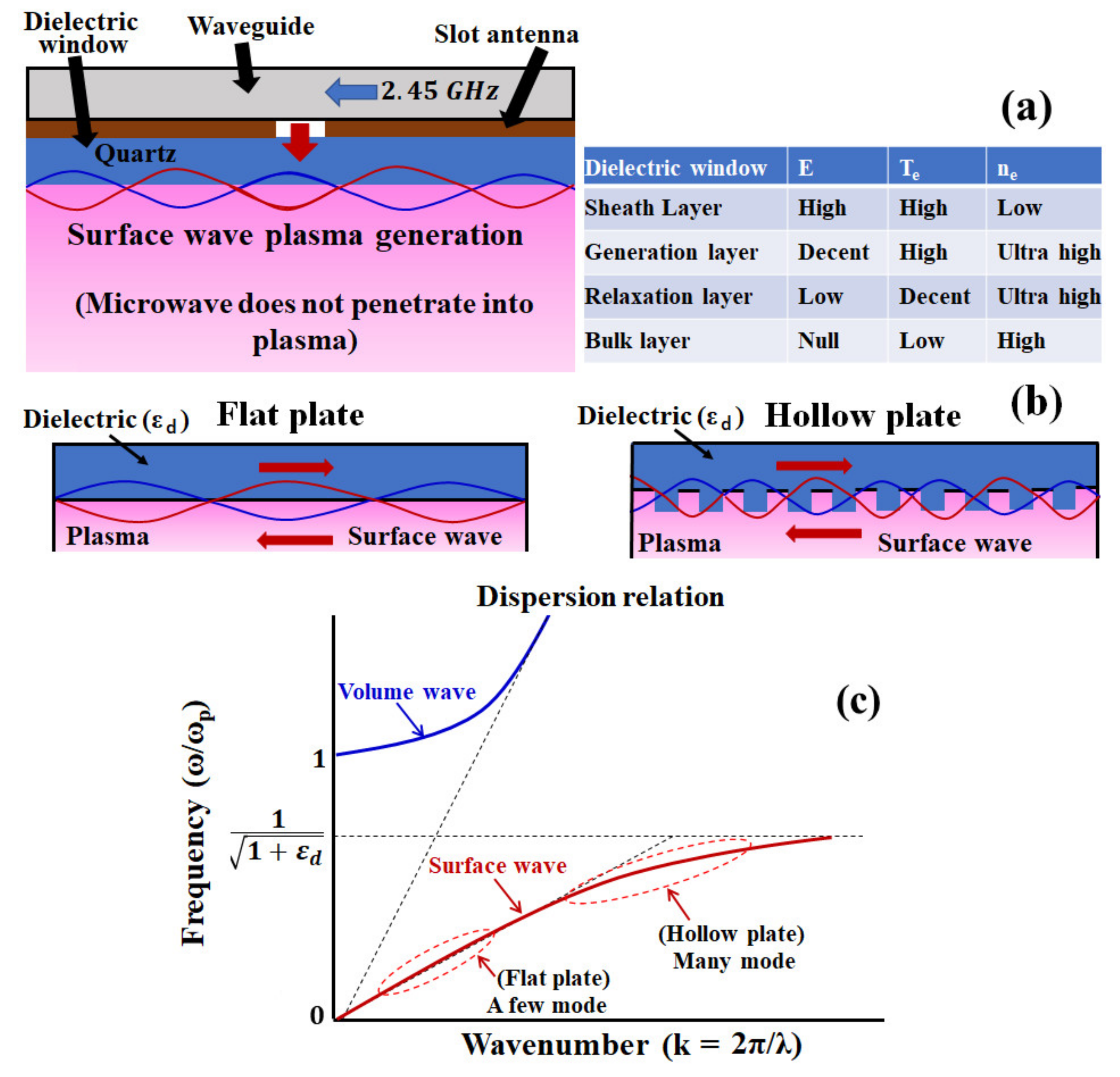
2. Microwave-Excited Surface Wave Plasma CVD (MW-SWP CVD)

The high-density, low-temperature, and large-area of plasma are important requirements in many processes, such as ultra-large-scale integrated circuits (ULSIs), fabrication of insulation layer, deposition of microcrystalline silicon for solar cell applications, carbon films, etc. [102,103,104,105,106,107,108]. Among various other plasma sources, surface-wave plasma (SWP) excited at a microwave frequency has been developed for generating high density, low temperature, and large-area plasma at a suitable chamber pressure [109,110,111,112,113,114,115,116,117]. In the SWP source, a microwave of frequency 2.45 GHz is guided using a waveguide, as shown in Figure 1a. A dielectric plate (usually quartz) is provided from the slot antenna at the bottom of the waveguide. When a strong electromagnetic wave is applied from the slot antenna through the dielectric plate, the electrons are accelerated by the field of the wave, causing ionization to generate and maintain plasma. Various types of antenna configurations have been used to generate plasma, such as planar slot antenna, annular slot antenna, spoke antenna, ring slot antenna, cylindrical microwave launchers, adjustable array antenna, and radial line slots [117,118,119,120,121,122,123,124]. Generally, a microwave frequency of 2.45 GHz was used in the SWP system, however, application of 915 MHz excitation frequency has also been demonstrated to achieve plasma enlargement with good uniformity [114]. A vacuum waveguide system has been used to eliminate the atmospheric pressure force exerted on a large dielectric plate for surface wave propagation, by which large-area SWP production has been realized. Production of plasma with 1 m length and 0.2 m width has been demonstrated using the vacuum waveguide system [115]. The vertical distance of the generated plasma can be termed as sheath layer, generation layer, relaxation layer, and bulk plasma, where the electric field (E), temperature of electron (Te), and electron density (ne) varies significantly in each layer. There is a sheath layer formation just below the dielectric window, where the E and Te are high and ne is low. Further, there are plasma generation layers and relaxation layers with width in several mm, followed by the bulk plasma layer [102]. The dielectric window of the surface wave plasma system can be flat and hollow types, where the generated standing wave can be significantly different. Figure 1b shows the schematic for the flat and hollow plates for plasma generation. It has been observed that the density jump disappears in the case of the hollow plate and plasma can smoothly start from low power [115].
Figure 1c shows the dispersion relation of electromagnetic waves in plasma. In general, the dispersion relation represents the relationship between frequency and wave number of electromagnetic waves propagating in plasma. Here, the vertical axis shows the value of the angular frequency (ω) of the wave, standardized by the electron plasma angular frequency (ωp), whereas the horizontal axis shows the wavenumber ( k = 2 π λ ;   λ   i s   w a v e l e n g t h ) . Since the value of ωp is proportional to the square root of the plasma density, when the plasma density is low for frequency ω ω p > 1 , it is almost similar to no plasma and the electromagnetic wave passes through the plasma (in this case the electromagnetic wave is called a volume wave). However, in case of frequency, ω ω p < 1 for high-density plasma, electromagnetic waves cannot penetrate the plasma and become surface waves that propagate along the interface between the dielectric plate and the plasma. As shown by the dashed line in Figure 1c, when this surface wave is ω ω p = 1 1 + ε d 1 / 2 , the wave length becomes infinitesimal ( k   i s   I n f i n i t y ) , which is called surface wave resonance. Here, ε d is the relative permittivity of the dielectric plate, where generally used quartz plate relative permittivity is ε d = 3.8. If the plasma density that gives surface wave resonance is n s w , then for ω = 2 π f , it can be expressed as
n s w = 1.24 × 10 8 1 + ε d f 2 c m 3
For example, applying a microwave frequency of 2.45 GHz on the quartz plate, the resonance density can be calculated as 3.57 × 1011 cm−3 from the above equation. From this, it can be observed that the plasma density reaches at least 3.57 × 1011 cm−3 by changing from the low-density volume wave mode to the high-density surface wave mode [124]. Further, the plasma density can be significantly differed for a flat plate and a hollow plate. It has been observed that using a flat plate, the plasma tends to localize around the multi-slot antenna at a high pressure, which can be overcome by using the multi-hollow window (MHW) technique. It has been obtained that the plasma with extremely high density can be locally produced inside the hollows [124]. Such widely-spread, high-density plasma spots make the global plasma distribution more uniform than in the flat window case. Thus, the hollow dielectric quartz plate placed bellow the slot-antenna can generate high density uniform plasma in a large area for the MW-SWP CVD method.
For promoting large-scale plasma accumulation and high-density plasma, MW-SWP systems have the following advantages:
(1) In the case of RF discharge, whether it is capacitive or inductive coupling, the excited antenna has almost the same metric size as plasma. In contrast to RF discharge CVD, the surface wave excited from a small antenna propagates and creates plasma, which can be enlarged in a large area for a MW-SWP CVD.
(2) The surface wave plasma (SWP) becomes a high-density plasma exceedingly at least 1011 cm−3 as derived from the above presented equation for surface wave resonance.
(3) In capacitively coupled RF discharge, the plasma potential is high and the ion impact energy to the CVD film is large, so damage to the film is likely to occur. On the other hand, the ion impact energy in the MW-SWP process is small, thereby a damage-free film can be synthesized [120,125,126,127].
Further, the roll-to-roll deposition process using MW-SWP CVD has been investigated, where uniform plasma generation is an important aspect to achieve homogenous growth of the materials [97]. Uniform and control growth of graphene, hBN, and other layered materials are still an important subject of research for the MW-SWP CVD method. We expect that the plasma method can be further improved to grow various materials independent of catalytic and noncatalytic substrates.

3. Growth of Graphene and 2D Materials

Growth of graphene by the plasma CVD process can be achieved on various substrates, such as metals, insulators, and semiconductors, at a significantly lower temperature than the thermal CVD process [74,75,76,77,78,79,80]. Moreover, synthesis of 2D materials, such as hBN, has been achieved by the plasma CVD technique [125]. Synthesis of graphene and hBN films has mostly been investigated on transition metal catalysts (such as Cu, Ni, Mo, etc.) or their alloy substrates (e.g., NiCu, NiMo, CuSn, etc.) in a CVD process [62,63,64,65,66,67,68,69,70]. The graphene synthesis on Cu substrate is significantly investigated due to their low carbon solubility and surface mediated catalytic growth of graphene layers. In another prospect, graphene films can be directly grown on a noncatalytic substrate by the plasma CVD techniques, considering the decomposition of precursor gas molecules in the plasma and forming plasma radicals for graphene growth at a considerably lower temperature [126]. In the following, we discuss the details of the plasma CVD process, most importantly the MW-SWP CVD technique for graphene-based materials synthesis.

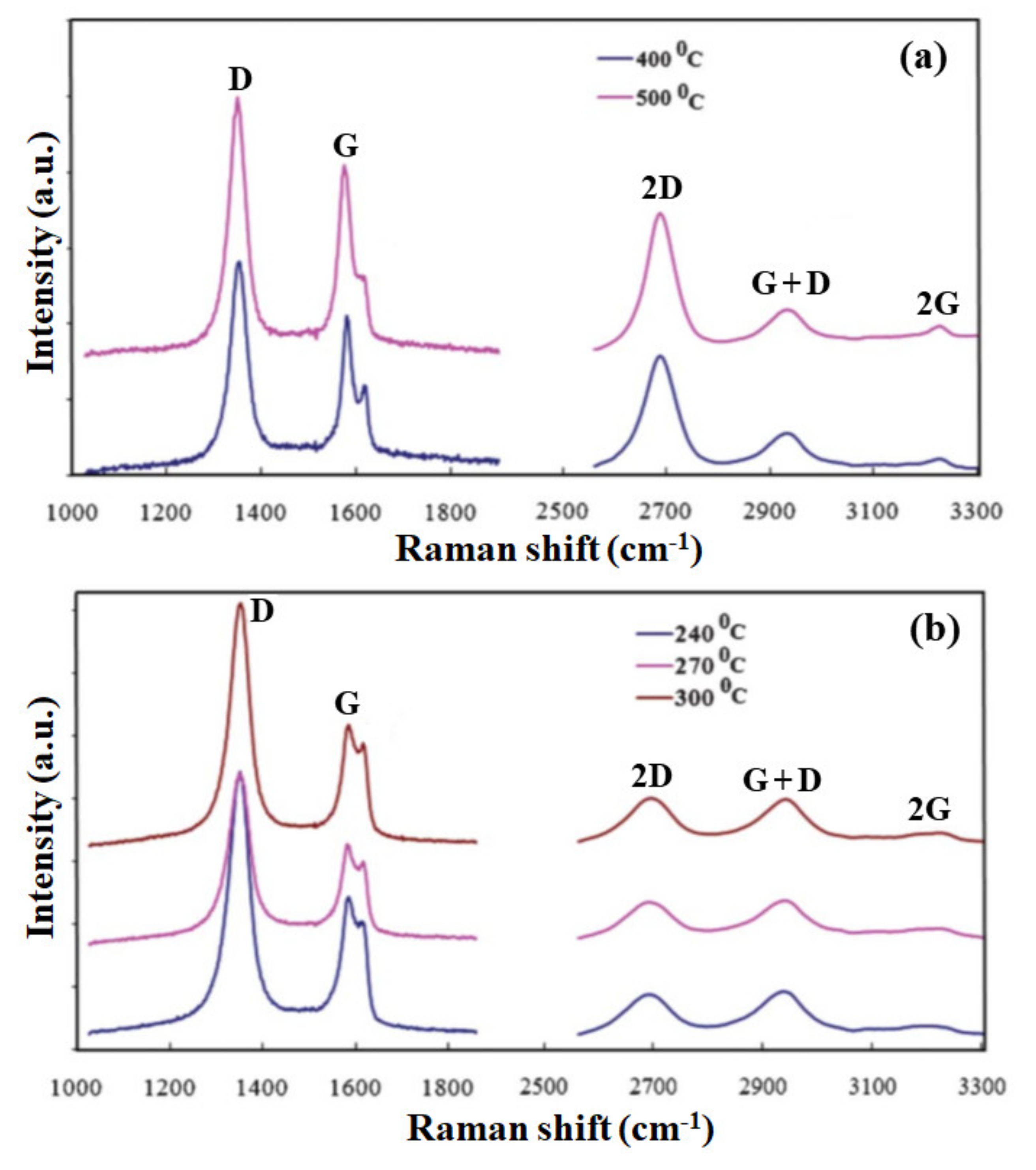
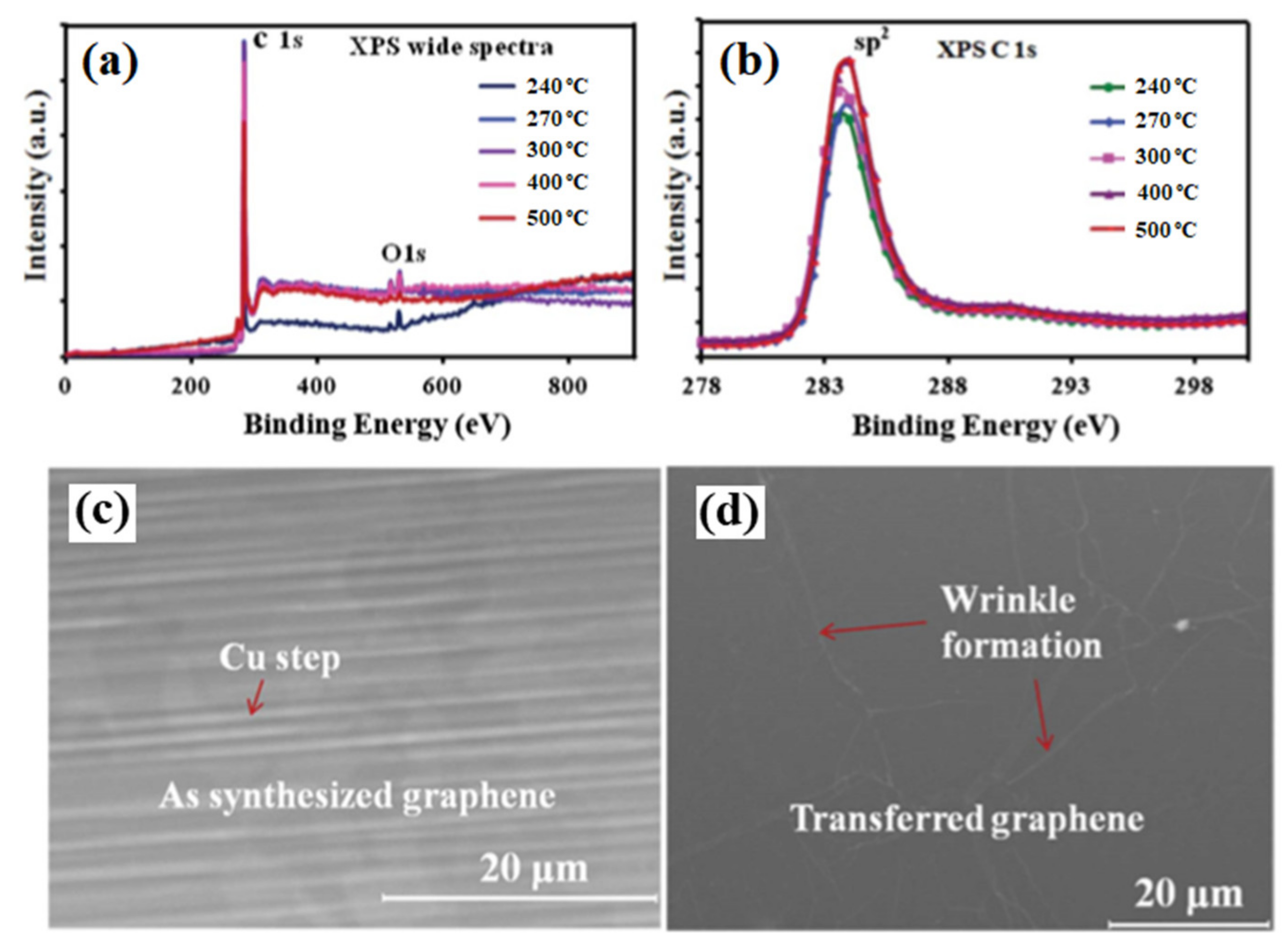
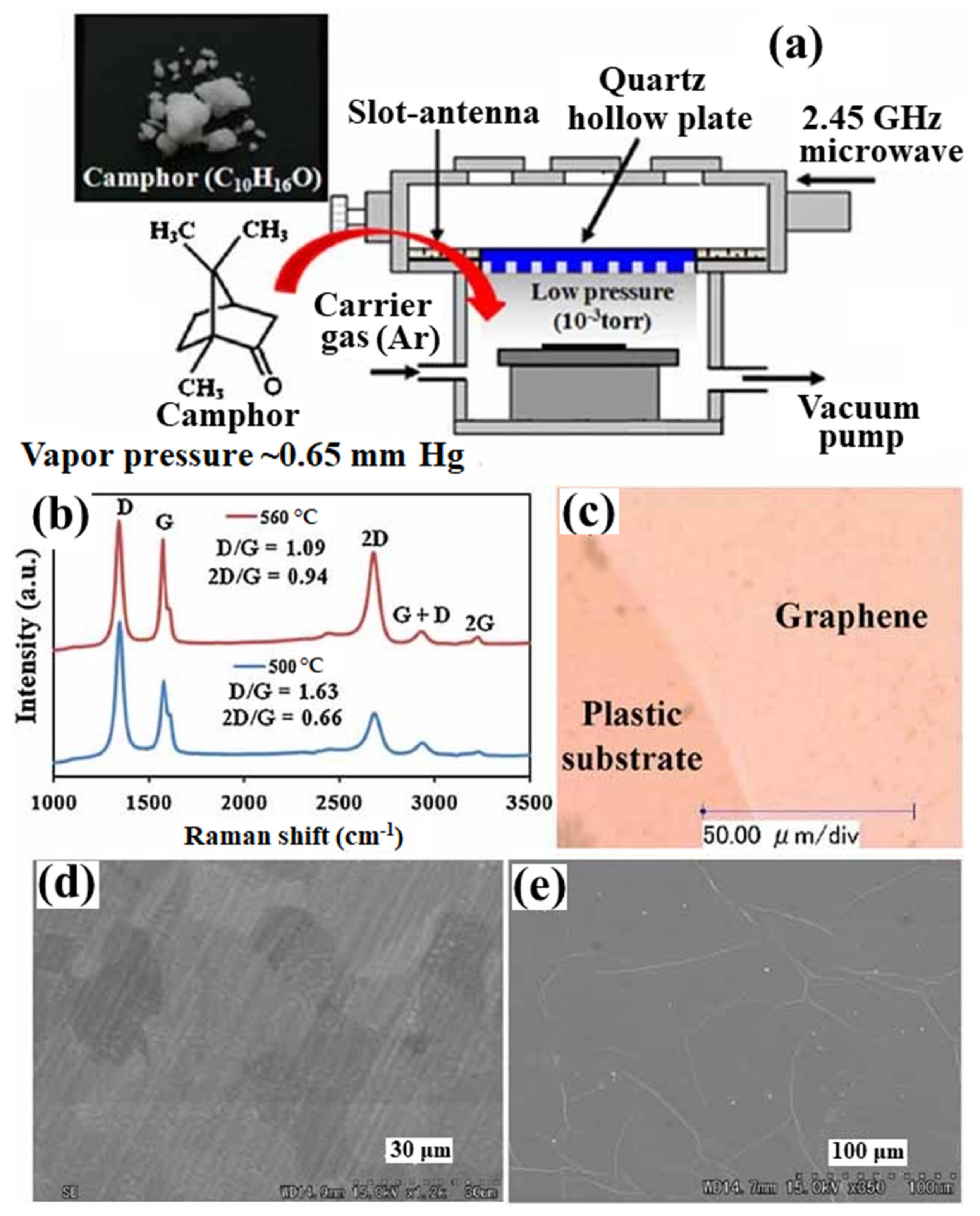
3.1. Growth of Graphene Films on Catalytic Substrates

Synthesis of a monolayer graphene film by the microwave plasma CVD (MWP CVD) process has been demonstrated on Ni foil at a temperature of 450 °C [127]. Subsequently, graphene synthesis by the MW-SWP CVD technique was developed, considering the advantage of large-scale growth at a significantly lower temperature (300–400 °C) [128]. Synthesis of few-layer graphene film on the Cu foil was achieved by the developed MW-SWP CVD process. The graphene film with excellent transparency and electrical conductivity is demonstrated for transparent electrode applications, which can be used in optoelectronics and nanoelectronics devices. The synthesized graphene on Cu and Al foil by the MW-SWP CVD process was analyzed by Raman spectroscopy. It was obtained that the synthesized graphene films were of few-layer structures. The intensity of the 2D peak is significantly higher than the G peak, which significantly differs from the monolayer graphene synthesized by the thermal CVD process. Similarly, Raman analysis confirms graphene film growth on the Al foil by the MW-SWP CVD technique. The spatial distribution of sheet resistance for the transferred graphene film was analyzed, which was found to be in the range of 1.0 to 4.1 kΩ/Sq over the area of 23 × 20 cm2 [128].
Synthesis of graphene films by similar MW-SWP CVD system was demonstrated by our group using gaseous and solid precursors at a lower substrate temperature [121,122,123,124]. Graphene growth was achieved on Cu foil without any pretreatment at a gas composition pressure of 45 Pa, a microwave power of 1.2 kW, and a growth duration of 2–4 min. Figure 2a shows the Raman spectra of the graphene films deposited at a substrate temperature of 400 and 500 °C. Further, Figure 2b shows the Raman spectra at a substrate temperature of 240, 270, and 300 °C, indicating the presence of a 2D peak and formation of a few-layers of graphene film. As presented in the figure, a disorder-induced D band is observed at approximately 1348 cm−1, indicating phonon scattering at defect sites and impurities. An intense graphitic G band is also observed at approximately 1574 cm−1, attributing to the sp2 phonon vibrations. Three other peaks were observed at approximately 2685, 2914, and 3210 cm−1, corresponding to 2D, G + D, and 2G second-order Raman spectra, respectively. The presence of a 2D and a 2G peak indicates good agreement of the graphene structure formation in the carbon film. The Raman characteristic for the graphene film deposited at 400 and 500 °C is almost identical, having a similar G and 2D peak intensity. The D and D + G peaks presented defect related structures in the sp2 hybridized graphene film [129].
The synthesized graphene films were analyzed by XPS and SEM to determine the chemical and the morphological structures. Figure 3a,b shows the wide XPS spectra and C1s spectra for different substrate temperatures. The XPS analysis shows a small oxygen (O1s) peak along with the dominant C1s peak. No other difference in chemical composition was observed for all the graphene samples. Figure 3c shows the SEM images of the as-synthesized graphene film on Cu foil at 240 °C, presenting graphene grain and Cu steps. Figure 3d shows the SEM image of transferred graphene film on a plastic substrate presenting wrinkle formation, which is a common feature for the transferred graphene film [129].
Figure 4 shows the schematic presentation of the MW-SWP CVD method for graphene synthesis using camphor as a solid precursor [130]. In this approach, solid camphor powder was directly inserted in the MW-SWP CVD chamber as carbon precursor. The camphor powder easily evaporated inside the CVD chamber and diluted with Ar gas to generate plasma. Figure 4a shows the Raman spectra of the synthesized graphene films on Cu foil at temperatures of 500 and 560 °C. Figure 4b shows the optical microscope image of graphene film transferred on plastic substrate. A continuous film with high transparency and conductivity was obtained on the plastic substrate. Figure 4c shows the SEM image of the as-synthesized graphene film on the Cu foil, where domain like structures of the graphene film can be observed. Figure 4d shows the SEM image of the transferred graphene film. The formation of wrinkles in the graphene film can be observed from the SEM analysis. The formation of such wrinkles in the transferred graphene film is consistent for the MW-SWP CVD synthesized samples, which is also the case for other CVD synthesized transferred graphene films [126]. Further, PMMA has been used as precursor coated on Cu foil for graphene synthesis by MW-SWP CVD method. Formation of graphene was confirmed at a substrate temperature as low as 280 °C. The Raman peak obtained on various positions of the sample was almost similar considering the uniform growth of the few-layer graphene with homogenous distribution of plasma [131]. Synthesis of the bilayer graphene using PMMA and CH4 as precursor has been demonstrated by the MW-SWP CVD at a significantly lower temperature. It has been observed that a carrier mobility of 740 cm2 V−1 s−1 can be obtained for the bilayer graphene synthesized by MW-SWP CVD method [83]. Ichimura et al. have demonstrated obtaining maximum Hall mobility of approximately 625 cm2 V−1 s−1 for the synthesized thin graphitic film by the MW-SWP CVD method [98]. Further, Hall mobility of approximately 398 cm2 V−1 s−1 has been obtained for a carbon dot doped graphene film synthesized by the MW-SWP CVD method [132,133]. It has been obtained that low carbon precursor concentration can be ideal for controlling the graphene domain growth with particular layer numbers [134]. Although few-layer graphene film can be synthesized on metal catalytic substrate by the MW-SWP CVD method at a significantly lower substrate temperature, control growth of monolayer graphene still remains a significant challenge. These studies gave a detailed overview of graphene synthesis by the MW-SWP CVD process for graphene growth on a catalytic metal substrate using the gaseous, solid, and other precursors. The graphene growth in MW-SWP CVD technique can be further investigated for control layer growth with larger grain size on metal catalytic substrates. In this prospect, effect of plasma interaction with the substrate surface can be critical, where the plasma radicals play a dominant role in graphene nucleation and growth.

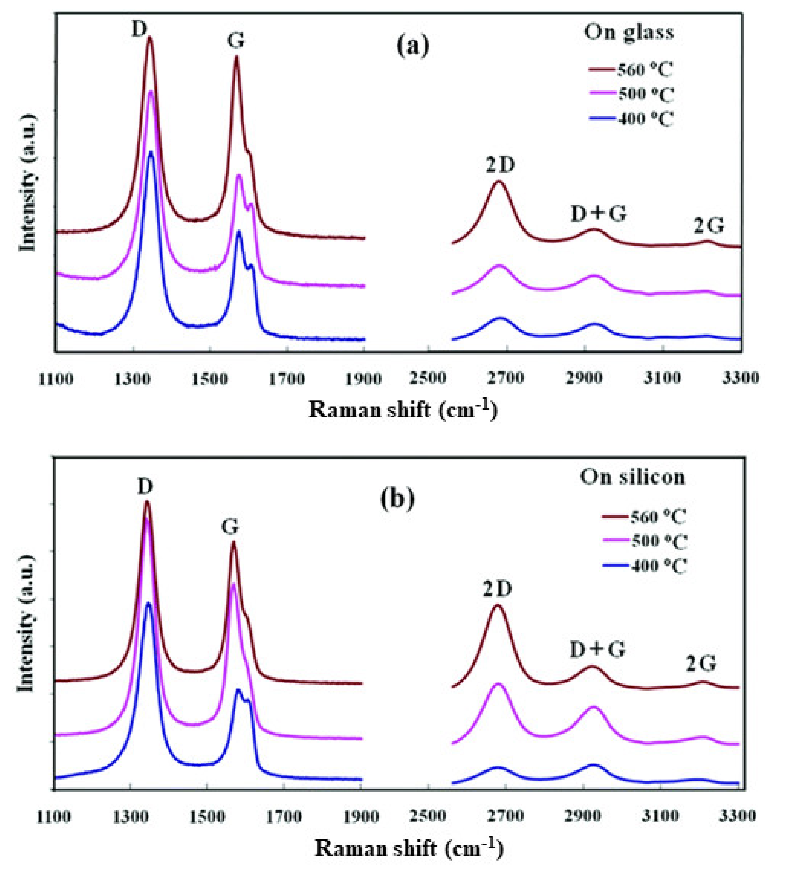
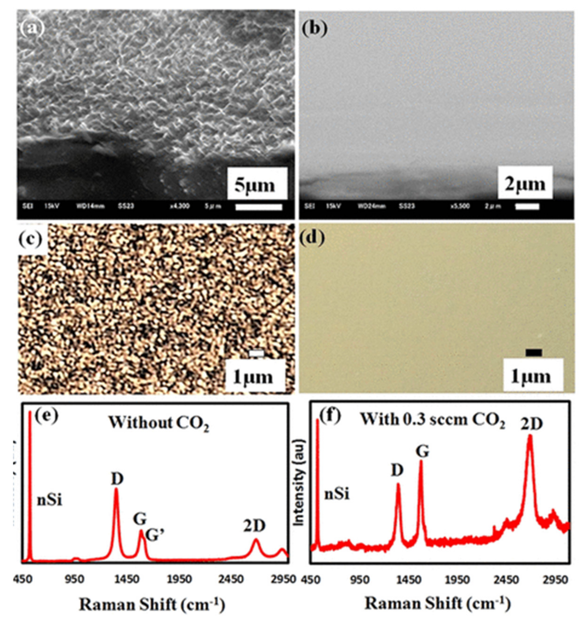
3.2. Direct Growth of Graphene on Arbitrary Substrates

Synthesis of graphene film directly on semiconducting, insulating, and dielectric substrates by the plasma CVD process is of great interest to avoid the transfer process and enabling direct integration in electronic devices. Synthesis of the graphene film on an arbitrary substrate by the MW-SWP CVD technique was demonstrated by our group [135]. The graphene film was synthesized using a gas mixture of C2H2 and Ar with gas composition pressure of 45 Pa and for a growth duration of 70–120 s. Figure 5 shows the Raman spectra of graphene films deposited on glass and silicon substrates at 400, 500, and 560 °C by the developed MW-SWP CVD method. Figure 5a shows the Raman studies of the carbon films deposited on glass substrates at different temperatures. The Raman spectra showed a strong and sharp graphitic G band at approximately 1568 cm−1, representing the crystalline sp2 hybridized carbon atoms for the nanographene domains. A disorder-induced D band is observed at 1339 cm−1; the high intensity of the D peak originates from either the small crystallite sizes or an abundance of edges in the nanographene structures. Three other peaks are observed at 2669, 2915, and 3214 cm−1, corresponding to 2D, G + D and 2G second-order Raman peaks. The presence of a distinct 2D peak confirmed the presence of a graphene structure in the synthesized carbon films. Similarly, Figure 5b shows the Raman studies of the carbon films deposited on silicon substrates, presenting the D, G, and 2D peaks at approximately 1341, 1566, and 2665 cm−1, respectively. The Raman studies showed that the structure of the nanographene film is similar and independent of the Si or SiO2 substrates. The graphene film deposited at 560 °C showed a greatly enhanced 2D peak, and a more suppressed D + G peak compared to those of the low temperature deposited films, indicating a more ordered graphene structure. These studies presented that the CVD process can be used for direct deposition of nanographene films on different substrates without using a metal catalytic layer. The deposition of a graphene film on a noncatalytic substrates is due to formation of carbon radicals with hydrogen termination in the microwave plasma, which plays a key role in the nucleation and growth process on the metal-free substrate surfaces. The carbon radicals of the plasma absorb onto the substrate surface and bonds to other such radicals by a diffusion process to form sp2 carbon [135].
The synthesized graphene films were characterized by transmittance and electrical conductivity analysis. The graphene films were highly transparent to visible light as it was synthesized for very short duration. Figure 6a shows the transmittance of the nanographene films deposited at 560 °C for different durations in comparison to indium tin oxide (inset of the figure shows a photograph of nanographene film deposited on the SiO2 substrate). The transmittance of the graphene film deposited for the shortest duration was 82% at a wavelength of 550 nm. Figure 6b shows the J-V characteristics of the fabricated devices with nanographene films deposited for different durations. As the thickness of the deposited graphene film increased with an increase in growth time, the conductivity of the graphene film increased. The graphene films obtained on the glass and silicon substrates can be significant for various device applications. Further, the developed process paves the way to deposit graphene film on an arbitrary substrate depending on application in optoelectronic and nanoelectronic devices. In the following, we discuss the fabrication of a graphene/silicon Schottky junction solar cell for a deposited nanographene film directly on silicon substrate. A photovoltaic device was configured with the directly grown nanographene film on the n-silicon substrate. Figure 6c shows a schematic diagram of the fabricated nanographene/n-silicon heterojunction device. The incident light in the device can transmit through the transparent graphene film and be absorbed in the n-silicon to generate photo-exciton. Figure 6d shows an energy band diagram of the nanographene/n-silicon photovoltaic device in thermal equilibrium. Due to the metallic nature of the graphene film, a Schottky junction can be formed with the n-silicon substrate. Several studies have shown that a thermal CVD synthesized graphene film can be transferred on the silicon substrate to form a Schottky junction device, creating a large built-in field (Vbi, 0.55–0.75 V) [136,137]. Due to the presence of a large built-in field in the graphene/n-silicon junction there can be efficient charge separation and transportation. Figure 6e shows a log scale plot for the dark J-V characteristics of the fabricated nanographene/n-silicon device. A device ideality factor of 2.44 was calculated from the J-V log plot as in the inset of Figure 6e. The fabricated device was characterized under illumination of white light with an intensity of 100 mW/cm2. Figure 6f shows the J-V characteristics of the graphene/silicon Schottky junction, presenting a photovoltaic action with a conversion efficiency of 2.1%. Recently, it has been demonstrated that a solar cell conversion efficiency can be achieved more than 6% for the directly grown graphene film by the MW-SWP CVD on silicon substrate [138]. Further, synthesis of graphene on catalytic/noncatalytic substrates has been investigated using LASER irradiation on substrate surface in the MW-SWP CVD method. It has been observed that graphene growth can be achieved under LASER irradiation, whereas graphene growth was not observed only with the plasma process for the particular growth conditions [139]. These studies are significant for direct growth of graphene structures on noncatalytic semiconducting, insulating, and dielectric substrates for potential applications in optoelectronic, sensor, solar cells, and heterojunction devices. Further, synthesis of graphene with control growth orientation can be a significant aspect to utilize the graphene surface for application in energy storage and conversation devices.

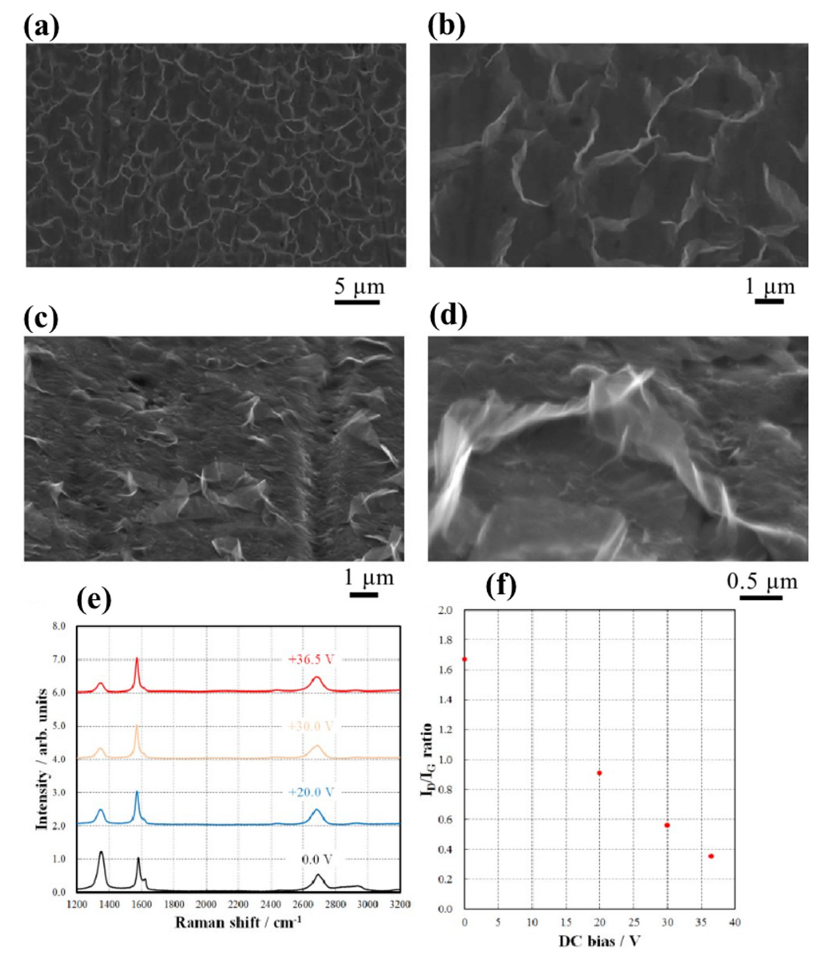
3.3. Growth of Vertically-Oriented Graphene

Synthesis of vertically-oriented carbon nanowalls on various substrates has been significantly explored by different CVD techniques [133,140,141,142,143]. The carbon nanowalls are vertically oriented graphene nanosheets with large surface area and high aspect ratio. Control growth of carbon nanowalls has mostly been demonstrated by a plasma CVD method, where wall to wall distances can be controlled with plasma parameters. Among various other plasma CVD techniques, MW-SWP CVD has been successfully used to synthesize carbon nanowalls on catalytic and noncatalytic substrates. Vertically oriented graphene growth was studied under direct current (DC) bias voltage by the developed MW-SWP CVD method. An external DC power supply was used to bias the substrates for synthesis of a graphene film [133]. The deposition was carried out at a substrate temperature of 650 °C, with a gas mixture of C2H2, Ar, and H2. Formation of graphene nanowalls on silicon substrate was confirmed by SEM analysis. Figure 7a–d shows the SEM image of graphene nanowalls synthesized by the MW-SWP CVD technique for various tilted angles of the substrate. Figure 7d clearly shows an upward growth orientation of the graphene layer from the substrate surface. The graphene nanowall samples were analyzed by Raman analysis. Figure 7e showed the Raman spectra of the synthesized vertically-aligned graphene at different applied DC bias voltages. Figure 7f shows the ID/IG ratio of Raman peak for the vertically-aligned nanowalls at different applied DC bias voltages. Raman spectra of the graphene nanowalls showed two main Raman peaks at approximately 1580 and 1350 cm−1, corresponding to the graphitic and defect related band of the synthesized carbon structures. The other Raman peak observed at approximately 1620 cm−1 can be identified as a defect related peak for the graphene structures of the nanowalls [133]. These results confirmed the possibility of synthesizing the vertically oriented graphene nanowalls by the MW-SWP CVD method. Further, investigations were carried out on the plasma CVD conditions for controlling the growth of planar graphene and vertically orientated graphene structures.
As discussed above vertically aligned graphene sheets were synthesized by the MW-SWP CVD method using substrate bias voltage. In another prospect, synthesis of vertically oriented graphene by the MW-SWP CVD method without using substrate bias voltage and using different gas composition has been demonstrated. It has been observed that the growth of planar graphene and vertically oriented graphene can be obtained by the plasma CVD method with or without CO2 gas along with CH4, H2, and Ar gas. Figure 8a shows a typical cross-sectional SEM image of a silicon sample with graphene deposition without CO2 clearly showing vertically grown structures, whereas in Figure 8b a cross-sectional SEM image of the sample with CO2 showed that there is no such vertical growth. Figure 8c,d shows the top view optical image of the same graphene samples, revealing differences in surface morphologies of sample surfaces after deposition without and with CO2. In the growth process, CO2 can etch the additional carbon atoms to prevent vertical growth of graphene layers and preserving the lateral growth of the graphene film. The Raman spectrum in Figure 8e shows a higher D peak with G′ and diminished 2D peaks, indicating the formation of a graphene structure with higher defects and disorders. This can also be correlated with the nonplanar graphene structure as observed from SEM analysis, where oriented graphene layers were formed on the substrate surface. Figure 8f shows Raman analysis of the graphene film deposited with the addition of 0.3 sccm CO2 gas along with the CH4, H2, and Ar gas. The Raman spectra showed a high intensity G and 2D peak in comparison to the graphene film deposited without CO2. The Raman G and 2D peak intently is almost equal, where D peak intensity is less than the G and 2D peak, indicating formation of thin graphene film [144]. These above discussed studies showed the possibility of using the MW-SWP CVD method to synthesize vertically oriented graphene films and other controlled structures of graphene-based materials.

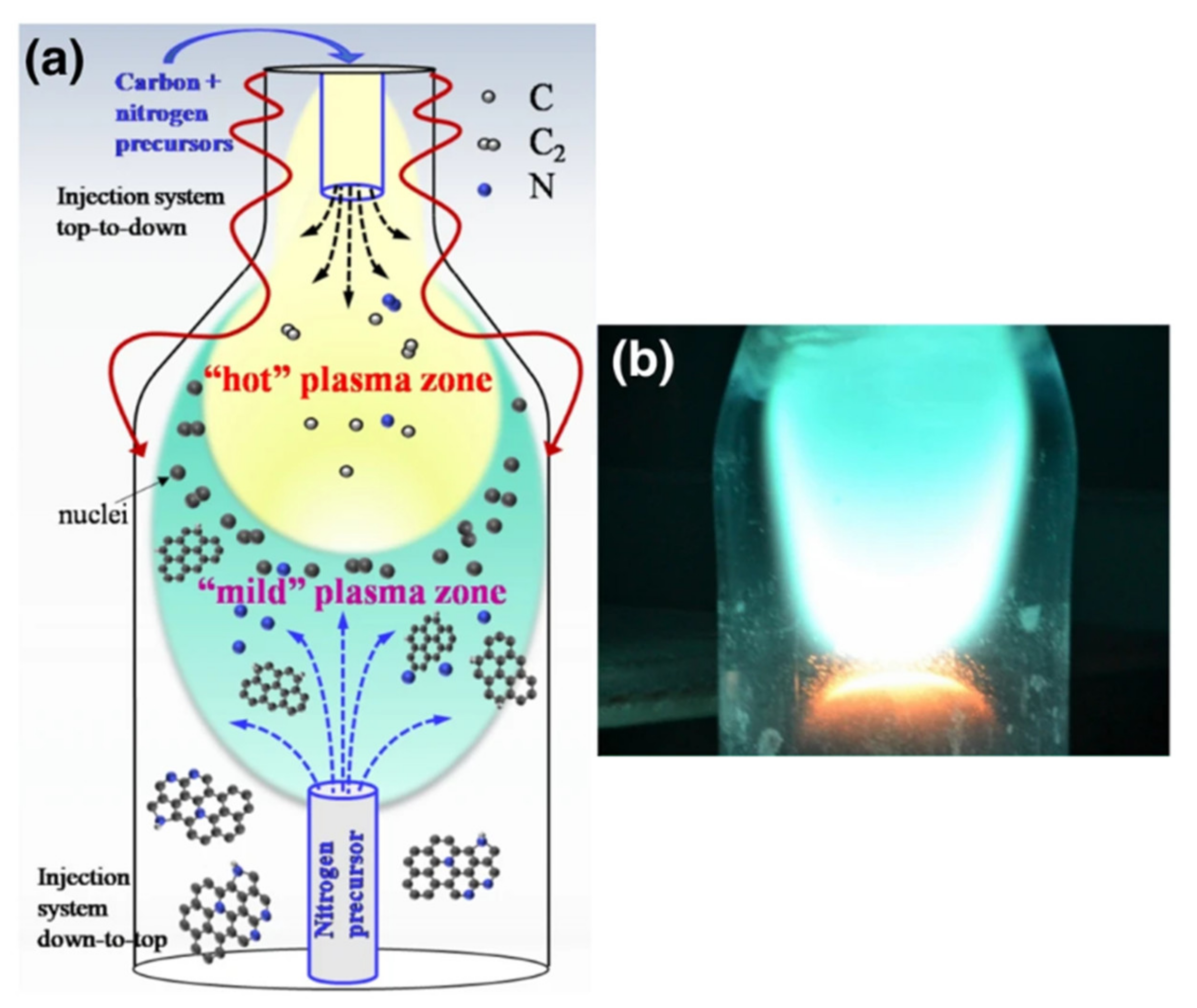
3.4. Doping of Graphene with Heteroatoms

The doping of a graphene layer is of significant importance to tune the electrical, mechanical, thermal, and chemical properties. Several dopant elements, such as nitrogen (N), boron (B), sulfur (S), phosphorus (P), fluorine (F), etc., have been investigated to incorporate in the structure of graphene, thereby changing the intrinsic properties. Doping of graphene film can be achieved during the growth process and by a post growth treatment process. Several studies have been reported on incorporation of dopant in graphene structures by the thermal CVD growth method. In this approach, dopant element can be incorporated in the graphene lattice, edges and surfaces, which has been found to be effective to tune electronic and chemical properties [145,146].
Synthesis of N-doped graphene using a SWP reactor has been demonstrated, as shown in Figure 9a. [147]. The developed system consisted of a waveguide-based setup to create MW-SWP at atmospheric pressure conditions. The plasma discharge takes place inside a quartz tube inserted perpendicularly to the waveguide and directed downstream, as presented in Figure 9a. The MW-SWP reactor consists of hot and mild plasma zones, which is similar to the MW-SWP system for growth of graphene film, as described above. The N-doped graphene materials can be synthesized by injecting precursor materials from the top and bottom in the SWP plasma reactor. The nitrogen containing carbon precursors mixed with argon gas decomposed in the plasma reactor to form plasma radicals, which enabled nucleation and growth of the N-doped graphene flakes, as shown in Figure 9b. It has also been reported that the gas temperature changes radially due to the radial thermal losses in the SWP reactor, where the radial profile of the temperature is approximately parabolic. The nucleation and growth processes were strongly determined by kinetic and thermodynamic factors, as the structural qualities of targeted nanostructures was achieved via synergistic tailoring of the hot plasma environment and thermodynamic conditions in the mild zone of the plasma reactor. Thus, selective synthesis of the N-doped graphene sheets was achieved by tailoring the temperature gradients, density of carbon molecules, and their residence time in the plasma reaction zone of the developed MW-SWP reactor system [147,148,149].
The relative yield of N-doped graphene was ~0.5 mg/min using ethanol and methane as carbon precursors, where the ammonia and methylamine as nitrogen precursors. It should be noted that the selective synthesis of N-doped graphene sheets can be obtained in a very narrow range of discharge operational conditions. Figure 10a,b shows the SEM images of the N-doped graphene sheets synthesized by the SWP reactor using ammonia/methylamine as nitrogen precursors, presenting the typical morphology of synthesized graphene sheets. The synthesized materials have also been characterized by TEM analysis, as shown in Figure 10c,d. The size of the N-doped graphene sheets was in range of 100 to 200 nm, with clear monolayer to few-layer edge structures. Further, the TEM analysis showed the folded, overlapped, and wrinkled structures of the N-doped graphene sheets. The highly ordered lattice fringes indicated that the synthesized N-doped graphene sheets were well-crystallized. The N-doped graphene layer was also obtained by considering a top-to-down injection scheme, where the carbon/nitrogen precursors was injected into the hot plasma region. The synthesized free-standing N-doped graphene sheets also contained few-layer graphene structures, as confirmed by the Raman and TEM analyses. The XPS analysis showed that the use of methane/methylamine as carbon/nitrogen precursors significantly increased the graphene doping level. The N-doped graphene synthesized using the methane/methylamine precursor, contained a nitrogen doping level of 8 at %. Further, the N-doped graphene lattice structure contained more than 60% sp2 carbons, which is significant for synthesizing N-doped graphene with high crystalline quality. Thus, the SWP reaction process can be significant to synthesize doped graphene-based materials compared to other thermal and chemical approaches, considering a dry process without using external heating systems [147,148,149].

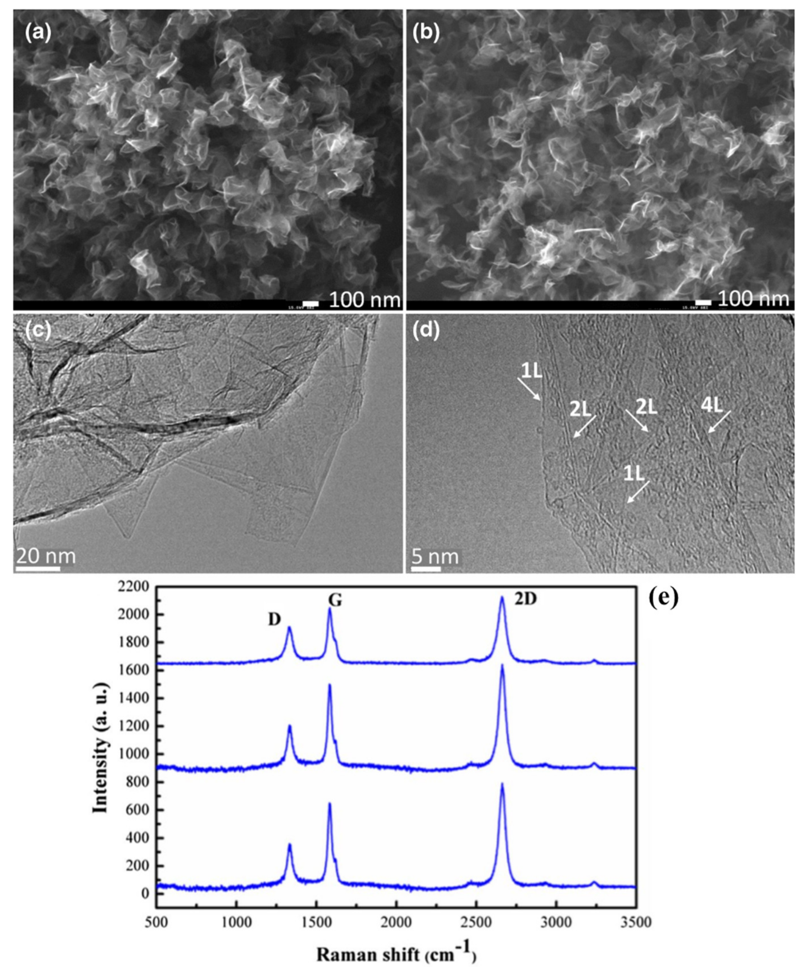
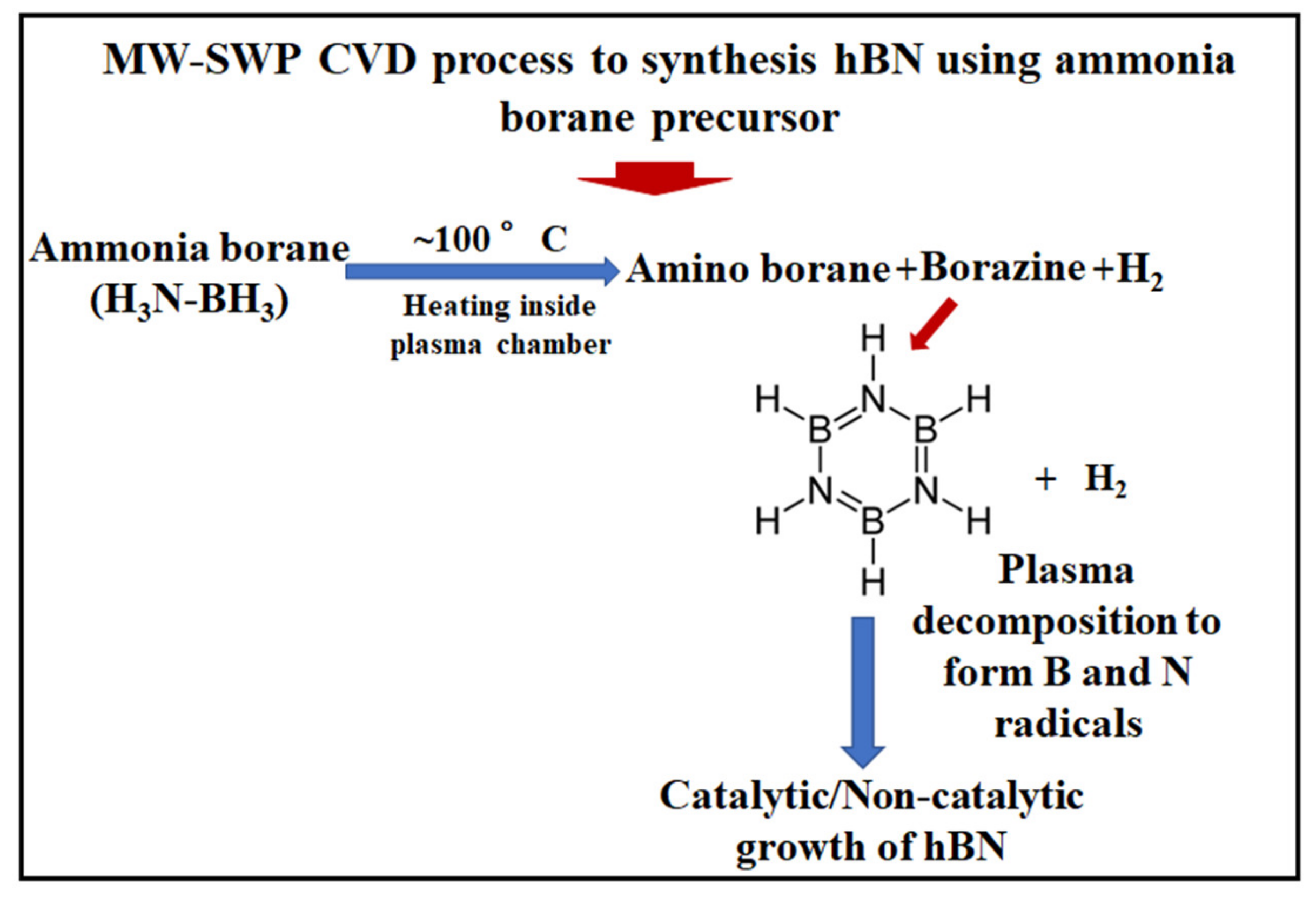
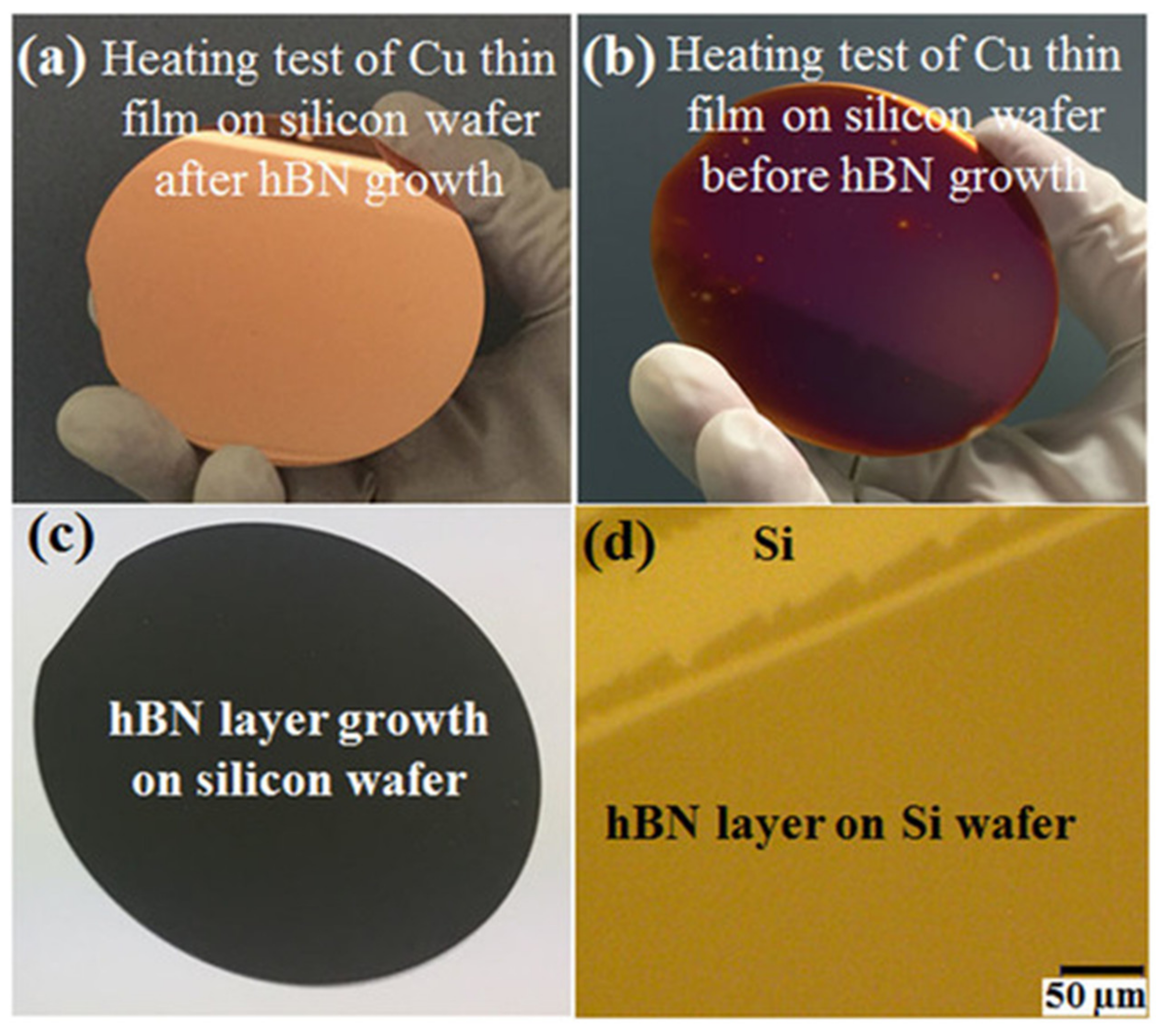
3.5. Growth of Boron Nitride (BN) Related Materials

Boron nitride (BN) based materials are covalently bonded ceramics belonging to the Group III nitrides. BN based materials possess many outstanding properties, such as chemical inertness, thermal conductivity, very good mechanical properties, and electrical insulating properties [150,151]. There are several polymorphs of BN, including amorphous BN (aBN), hexagonal BN (hBN), rhombohedral BN (rBN), cubic BN (cBN), and wurtzite BN (wBN). Among these polymorphs, the rBN and hBN are sp2 hybridized, whereas cBN and wBN are sp3-hybridization in their covalent bond [152]. Unlike graphite, BN is not found naturally and needs to produce from boron and nitrogen containing precursors. Different methods and experimental conditions have been established to synthesize BN from a variety of boron and nitrogen precursors. BN has been synthesized by high pressure/high temperature methods, which are generally expensive and difficult to produce in bulk quantity. Several studies have also been performed to synthesize large area hBN films by the CVD technique a under wide range of growth parameters and then that of the cBN and wBN based materials [152,153,154,155]. The hBN layer has been considered as an important dielectric material for fabrication of next generation field-effect transistors (FETs), with the potential for extending Moore’s law. Several studies have been carried out to synthesize monolayer, few-layer, and multi-layer hBN films by the CVD technique, using various kind of precursors. Mostly hBN polycrystalline as well as single crystalline domains and continuous films were synthesized on transition metal catalytic substrates (Cu, Ni, etc.) [151,152,153,154,155,156]. It has also been recognized that the highly uniform and multilayer hBN films can be more suitable for application in FETs and several other applications.
Synthesis of wafer scale hBN film by the MW-SWP CVD was investigated using the ammoniaborane solid precursor [156]. A silicon wafer of 3-inch diameter was taken as a non-catalytic substrate, while another silicon wafer coated with a Cu thin film on SiO2/Si wafer (Cu/SiO2/Si) was taken as the catalytic substrate. The substrates were placed inside the MW-SWP CVD chamber heating holder along with the precursor materials so that it could be easily sublimed inside the CVD chamber. The deposition of hBN film was performed by evaporating the ammonia borane precursor with dilution of Ar and H2 gases of 100 and 5 sccm flow rates, respectively. The growth duration was 3 min., with a fixed plasma power of 1000 W. Figure 11 shows a schematic representation of the ammonia borane precursor decomposition with a small heat from the substrate holder. The ammonia borane precursor sublimed in the chamber and decomposed to amino borane (BH2NH2), borazine, and release hydrogen gas. The generated precursor vapor was diluted with Ar and H2 gas mixture and plasma was generated in the chamber. The vaporized molecules were dissociated in the plasma to form N and B plasma radicals and interact with the substrate surface to form the hBN layer on Cu/SiO2/Si substrate. The hBN deposited Cu/SiO2/Si substrate was tested by heating at atmospheric conditions on a hot plate. Figure 12a shows a photograph of the heating test of Cu thin film on silicon wafer after hBN growth. There is no change in the color of the Cu thin film with the deposited hBN film, as the hBN film acts as a protective coating layer to oxidation of the Cu surface. Figure 12b shows the as prepared Cu/SiO2/Si wafer sample after the heating test in atmospheric conditions. Figure 12c shows the photograph of silicon wafer after directly depositing the hBN film using the ammonia borane precursor in the MW-SWP CVD process. A slight change in the color of the silicon wafer top surface was observed after the deposition of the hBN films. Figure 12d shows an optical microscope image of the hBN layer directly grown on the silicon wafer. The scratch line on the deposited film on the silicon wafer confirmed the growth of hBN film on the silicon wafer. There studies clearly showed growth of hBN film on catalytic and noncatalytic substrates using the ammonia borane as a solid precursor in the developed MW-SWP CVD method. Further, the synthesized materials were analyzed by microscopic and spectroscopic tools to confirm formation of the hBN layer [156].
The catalytically grown film was chemically etched and transferred on SiO2/Si substrate. Furthermore, Figure 13a shows the optical microscope image of the transferred hBN film on the SiO2/Si substrate. The optical microscopic image confirmed a continuous film structure, with folded edges. Figure 13b shows a SEM image of the transferred hBN film, presenting morphology of a continuous film. The optical microscope and SEM images confirmed the catalytic growth of an hBN layer at a comparatively lower temperature than that of the thermal CVD process, using the ammonia borane precursor. The bonding/chemical structures of the deposited hBN film was investigated by FTIR spectroscopic analysis. Figure 13c shows the FTIR absorption spectra of the synthesized hBN film on SiO2/Si substrate, comparing with an uncoated same substrate. A strong absorption peak appeared for the hBN coated sample at 1385 cm−1, which corresponds to the transverse optical (TO) vibrations for in plane B-N bond stretching in sp2 bonded hBN. The FTIR result clearly showed presence of hBN layered structure. Furthermore, the elemental composition along with the impurities was investigated by the XPS analysis. Figure 13d shows the XPS survey spectra for the catalytic and non-catalytic growth of the hBN samples. The XPS spectra shows clear B1s (191 eV) and N1s (401 eV) peaks along with the C1s (284 eV) and O1s (500 eV) peaks. Furthermore, we compared the individual B1s and N1 speaks of hBN film on the catalytic and non-catalytic substrates. Figure 13e-f shows the B1s and N1s core level spectra for the hBN synthesized on (Cu/SiO2/Si) and non-catalytic (SiO2/Si) substrates. The B1s and N1s peak-centers were observed at 191.1 and 398.5 eV, respectively, as calibrated for the C1s peak. The N1s and B1s peaks were almost similar for the both catalytic and non-catalytic growth, indicating no significant difference in the hBN structure. The incorporation of carbon and oxygen impurities in the highly reactive hBN sample might take place during the growth process and post-growth atmospheric exposure. It is observed that the oxygen and carbon impurities for the plasma deposited hBN film is higher than that of thermal CVD synthesized hBN from the XPS studies [144]. This is also an interesting fact that the plasma CVD process can be significant to incorporate doping impurities in hBN layers and can lead to synthesis of boron-carbon-nitride (BCN) and boron-carbon-nitride-oxide (BCNO) related structures with different composition and thereby tuning the electrical, chemical and thermal properties of the films [151,152,153,154,155,156].

4. Future Prospects of MW-SWP CVD for 2D Materials Synthesis

Table 2 summarized graphene growth by the MW-SWP CVD process in comparison to RF plasma and thermal CVD methods. The MW-SWP CVD method has been successfully established as a versatile CVD technique to grow graphene film on metals, semiconductors, insulators, and dielectric substrates independent of their catalytic and noncatalytic properties. However, controlling the crystalline quality and layer numbers for the synthesized graphene film is a significant challenge for the developed MW-SWP CVD method. Again, the electrical properties of the graphene film deposited by the plasma CVD method is not as good as the thermal CVD method as discussed above due to higher defects and smaller grain sizes, nevertheless application in various electronic devices can be explored considering the possibility of direct growth and thereby overcoming the influence of interface trap states due to impurities. Furthermore, controlling the vertically-aligned graphene sheet synthesis process can be significant, where spacing of graphene sheets, length, and adhesibility with substrate surface are key aspects for various prospective applications. The MW-SWP CVD method has been used to synthesize wafer-scale hBN film on the catalytic and noncatalytic substrates. The thickness of hBN film can be controlled and much thicker film can be synthesized in wafer scale compare to the thermal CVD process, as the monolayer and the few-layer hBN growth are limited by the catalytic growth nature of the substrate in a thermal CVD process. Further, graphene-like BCN structures and other 2D layered materials can be synthesized by the developed process as gaseous and solid precursor can be introduced in the growth chamber. Synthesis of graphene/hBN heterostructures and other heterostructures of 2D layered materials can be interesting prospects for future studies in MW-SWP CVD methods. Sulfurization of metal films and use of metal organic precursors can be interesting prospects for low temperature synthesis of TMDCs layers by the MW-SWP CVD method. The MW-SWP can be also an important technique for processing of graphene oxide, MXenes, oxide layered materials, and other nanomaterials. Recently, we demonstrated the near-room temperature reduction of graphene oxide films and doping of nitrogen atoms [38]. Interestingly, graphene oxide films coated on the flexible polymer substrates can be processed by MW-SWP, opening possibilities for the reduction and incorporation of doping elements in graphene oxide films on various soft substrates. In other prospects, MW-SWP process can be used for functionalizing, surface processing, encapsulation, and incorporation of doping elements, thereby expanding the application of plasma methods.

5. Conclusions

In this review article, we discussed the MW-SWP CVD process for growth of graphene and hBN related structures on various substrate materials, such as metal, semiconductor, and insulators. The MW-SWP CVD system, consisting of waveguide, slot antenna, and dielectric window is significant to generate high density uniform plasma in a large area. The surface wave plasma generation process is discussed from the dispersion relation of electromagnetic waves in plasma. Low electron temperature and high electron density plasma can be generated in the bulk plasma region, which is significant to synthesize 2D layered materials without affecting the substrate surface. This has enabled low temperature direct growth of the graphene and hBN films on metals, semiconductors, and insulating substrates. Furthermore, growth of graphene can be achieved with a particular orientation to the substrate surface, resulting in vertically-aligned graphene nanowalls. Doping of nitrogen in the graphene structures also demonstrated by the MW-SWP CVD method to obtain nitrogen doped graphene in powder form. These research findings on the synthesis of graphene and hBN with various forms and independent of substrate materials can be significant for application in photovoltaics, sensors, battery, supercapacitor, fuel cells, and various other electronic device applications.

Author Contributions

G.K. wrote the article and M.U. contributed in preparing the article. All authors have read and agreed to the published version of the manuscript.

Funding

This research received no external funding.

Institutional Review Board Statement

Not applicable.

Informed Consent Statement

Not applicable.

Data Availability Statement

The review article data are already published as referred in the article.

Conflicts of Interest

The authors declare no conflict of interest.

References

  1. Novoselov, K.S.; Geim, A.K.; Morozov, S.V.; Jiang, D.; Zhang, Y.; Dubonos, S.V.; Grigorieva, I.V.; Firsov, A.A. Electric field effect in atomically thin carbon films. Science 2004, 306, 666–669. [Google Scholar] [CrossRef] [PubMed]
  2. Zhang, Y.; Tan, Y.W.; Stormer, H.L.; Kim, P. Experimental observation of the quantum Hall effect and Berry’s phase in graphene. Nature 2005, 438, 201–204. [Google Scholar] [CrossRef] [PubMed]
  3. Stankovich, S.; Dikin, D.A.; Dommett, G.H.B.; Kohlhaas, K.M.; Zimney, E.J.; Stach, E.A.; Piner, R.D.; Nguyen, S.T.; Ruoff, R.S. Graphene-based composite materials. Nature 2006, 442, 282–286. [Google Scholar] [CrossRef] [PubMed]
  4. Geim, A.K.; Novoselov, K.S. The rise of graphene. Nat. Mater. 2009, 6, 183–191. [Google Scholar] [CrossRef]
  5. Castro Neto, A.H.; Guinea, F.; Peres, N.M.R.; Novoselov, K.S.; Geim, A.K. The electronic properties of graphene. Rev. Mod. Phys. 2009, 81, 109–162. [Google Scholar] [CrossRef]
  6. Morozov, S.V.; Novoselov, K.S.; Katsnelson, M.I.; Schedin, F.; Elias, D.C.; Jaszczak, J.A.; Geim, A.K. Giant intrinsic carrier mobilities in graphene and its bilayer. Phys. Rev. Lett. 2008, 100, 016602. [Google Scholar] [CrossRef]
  7. Du, X.; Skachko, I.; Andrei, E.Y.; Barker, A. Approaching ballistic transport in suspended graphene. Nat. Nanotechnol. 2008, 3, 491–495. [Google Scholar] [CrossRef]
  8. Lin, Y.M.; Dimitrakopoulos, C.; Jenkins, K.A.; Farmer, D.B.; Chiu, H.Y.; Grill, A.; Avouris, P. 100-GHz transistors from wafer-scale epitaxial graphene. Science 2010, 327, 662. [Google Scholar] [CrossRef]
  9. Eda, G.; Fanchini, G.; Chhowalla, M. Large-area ultrathin films of reduced graphene oxide as a transparent and flexible electronic material. Nat. Nanotechnol. 2008, 3, 270–274. [Google Scholar] [CrossRef]
  10. Cai, D.; Song, M.; Xu, C. Highly conductive carbon-nanotube/graphite-oxide hybrid films. Adv. Mater. 2008, 20, 1706. [Google Scholar] [CrossRef]
  11. Schedin, F.; Geim, A.K.; Morozov, S.V.; Hill, E.W.; Blake, P.; Katsnelson, M.I.; Novoselov, K.S. Detection of individual gas molecules adsorbed on graphene. Nat. Mater. 2007, 6, 652–655. [Google Scholar] [CrossRef]
  12. Raccichini, R.; Varzi, A.; Passerini, S.; Scrosati, B. The role of graphene for electrochemical energy storage. Nat. Mater. 2015, 14, 271–279. [Google Scholar] [CrossRef]
  13. Bae, S.; Kim, H.; Lee, Y.; Xu, X.; Park, J.-S.; Zheng, Y.; Balakrishnan, J.; Lei, T.; Kim, H.R.; Song, Y.; et al. Roll-to-roll production of 30-inch graphene films for transparent electrodes. Nat. Nanotechnol. 2010, 5, 574–578. [Google Scholar] [CrossRef]
  14. Li, X.; Zhu, H.; Wang, K.; Cao, A.; Wei, J.; Li, C.; Jia, Y.; Li, Z.; Li, X.; Wu, D. Graphene-on-silicon schottky junction solar cells. Adv. Mater. 2010, 22, 2743–2748. [Google Scholar] [CrossRef]
  15. Sun, X.; Gong, F.; Hao, M.; Wu, L.; Yin, C.; Sun, Z.; Xiao, R. Enhanced thermal transport and corrosion resistance by coating vertically-aligned graphene on zirconium alloy for nuclear reactor applications. Appl. Surf. Sci. 2022, 582, 152484. [Google Scholar] [CrossRef]
  16. Sadighbayan, D.; Khan, A.M.; Zadeh, E.G. Laser-induced graphene-functionalized field-effect transistor-based biosensing: A potent candidate for COVID-19 detection. IEEE Trans. Nanobiosci. 2022, 21, 232–245. [Google Scholar] [CrossRef]
  17. Vineesh, T.V.; Kumar, M.P.; Takahashi, C.; Kalita, G.; Alwarappan, S.; Pattanayak, D.K.; Narayanan, T.N. Bifunctional electrocatalytic activity of boron-doped graphene derived from boron carbide. Adv. Energy Mater. 2015, 5, 1500658. [Google Scholar] [CrossRef]
  18. Balandin, A.A.; Ghosh, S.; Bao, W.; Calizo, I.; Teweldebrhan, D.; Miao, F.; Lau, C.N. Superior thermal conductivity of single-layer graphene. Nano Lett. 2008, 8, 902–907. [Google Scholar] [CrossRef]
  19. Nair, R.R.; Blake, P.; Grigorenko, A.N.; Novoselov, K.S.; Booth, T.J.; Stauber, T.; Peres, N.M.R.; Geim, A.K. Fine structure constant defines visual transparency of graphene. Science 2008, 320, 1308. [Google Scholar] [CrossRef]
  20. Heersche, H.B.; Jarillo-Herrero, P.; Oostinga, J.B.; Vandersypen, L.M.K.; Morpurgo, A.F. Bipolar supercurrent in graphene. Nature 2007, 446, 56. [Google Scholar] [CrossRef] [Green Version]
  21. Ma, K.Y.; Zhang, L.; Jin, S.; Wang, Y.; Yoon, S.I.; Hwang, H.; Oh, J.; Jeong, D.S.; Wang, M.; Chatterjee, S.; et al. Epitaxial single-crystal hexagonal boron nitride multilayers on Ni (111). Nature 2022, 606, 88–93. [Google Scholar] [CrossRef] [PubMed]
  22. Mak, K.F.; Lee, C.; Hone, J.; Shan, J.; Heinz, T.F. Atomically thin MoS₂: A new direct-gap semiconductor. Phys. Rev. Lett. 2010, 105, 136805. [Google Scholar] [CrossRef]
  23. Wang, Q.H.; Kalantar-Zadeh, K.; Kis, A.; Colema, J.N.; Strano, M.S. Electronics and optoelectronics of two-dimensional transition metal dichalcogenides. Nat. Nanotechnol. 2012, 7, 699–712. [Google Scholar] [CrossRef]
  24. Desai, P.; Ranade, A.K.; Mahyavanshi, R.; Tanemura, M.; Kalita, G. Influence of MoS2-silicon interface states on spectral photoresponse characteristics. Phys. Status Solidi A 2019, 216, 1900349. [Google Scholar] [CrossRef]
  25. Mahyavanshi, R.D.; Kalita, G.; Sharma, K.P.; Kondo, M.; Dewa, T.; Kawahara, T.; Tanemura, M. Synthesis of MoS2 ribbons and their branched structures by chemical vapor deposition in sulfur-enriched environment. Appl. Surf. Sci. 2017, 409, 396–402. [Google Scholar] [CrossRef]
  26. Thangaraja, A.; Shinde, S.M.; Kalita, G.; Tanemura, M. An effective approach to synthesize monolayer tungsten disulphide crystals using tungsten halide precursor. Appl. Phys. Lett. 2016, 108, 053104. [Google Scholar] [CrossRef]
  27. Wang, X.; Meng, L.; Li, B.; Gong, Y. Heteroatom doped graphene engineering for energy storage and conversion. Mater. Today 2021, 47, 108–130. [Google Scholar] [CrossRef]
  28. Zhua, H.; Gan, X.; McCreary, A.; Lv, R.; Lin, Z.; Terrones, M. Heteroatom doping of two-dimensional materials. Nano Today 2020, 30, 100829. [Google Scholar] [CrossRef]
  29. Liu, X.; Zhang, N.J.; Watanabe, K.; Taniguchi, T.; Li, J.I.A. Isospin order in superconducting magic-angle twisted trilayer graphene. Nat. Phys. 2022, 18, 522–527. [Google Scholar] [CrossRef]
  30. Mahyavanshi, R.D.; Kalita, G.; Ranade, A.; Desai, P.; Kondo, M.; Dewa, T.; Tanemura, M. Photovoltaic action with broadband photoresponsivity in germanium-MoS2 ultrathin heterojunction. IEEE Trans. Electron. Devices 2018, 65, 4434–4440. [Google Scholar] [CrossRef]
  31. Turkel, S.; Swann, J.; Zhu, Z.; Christos, M.; Watanabe, K.; Taniguchi, T.; Sachdev, S.; Scheurer, M.S.; Kaxiras, E.; Dean, C.R.; et al. Orderly disorder in magic-angle twisted trilayer graphene. Science 2022, 376, 193–199. [Google Scholar] [CrossRef] [PubMed]
  32. He, M.; Li, Y.; Cai, J.; Liu, Y.; Watanabe, K.; Taniguchi, T.; Xu, X.; Yankowitz, M. Symmetry breaking in twisted double bilayer graphene. Nat. Phys. 2021, 17, 26–30. [Google Scholar] [CrossRef]
  33. Lyu, J.; Pei, J.; Guo, Y.; Gong, J.; Li, H. A New opportunity for 2D van der Waals heterostructures: Making steep-slope transistors. Adv. Mater. 2020, 32, 1906000. [Google Scholar] [CrossRef] [PubMed]
  34. Zhang, Y.; Tang, T.T.; Girit, C.; Hao, Z.; Martin, M.C.; Zettl, A.; Crommie, M.F.; Shen, Y.R.; Wang, F. Direct observation of a widely tunable bandgap in bilayer graphene. Nature 2009, 459, 820–823. [Google Scholar] [CrossRef]
  35. Rickhaus, P.; Zheng, G.; Lado, J.L.; Lee, Y.; Kurzmann, A.; Eich, M.; Pisoni, R.; Tong, C.; Garreis, R.; Gold, C.; et al. Gap opening in twisted double bilayer graphene by crystal fields. Nano Lett. 2019, 19, 8821–8828. [Google Scholar] [CrossRef]
  36. Mills, S.; Mizuno, N.; Wang, P.; Lyu, J.; Watanabe, K.; Taniguchi, T.; Camino, F.; Zhang, L.; Du, X. Contact transparency in mechanically assembled 2D material devices. J. Phys. Mater. 2019, 2, 035003. [Google Scholar] [CrossRef]
  37. Kalita, G.; Sharma, S.; Wakita, K.; Umeno, M.; Hayashi, Y.; Tanemura, M. A photoinduced charge transfer composite of graphene oxide and ferrocene. Phys. Chem. Chem. Phys. 2013, 15, 1271–1274. [Google Scholar] [CrossRef]
  38. Kalita, G.; Jaisi, B.P.; Umeno, M. Effective reduction and doping of graphene oxide films at near-room temperature by microwave-excited surface-wave plasma process. Diam. Relat. Mater. 2022, 126, 109066. [Google Scholar] [CrossRef]
  39. Radisavljevic, B.; Radenovic, A.; Brivio, J.; Giacometti, V.; Kis, A. Single-layer MoS2 transistors. Nat. Nanotech. 2011, 6, 147–150. [Google Scholar] [CrossRef]
  40. Mahyavanshi, R.D.; Kalita, G.; Singh, R.; Kondo, M.; Dewa, T.; Kawahara, T.; Umeno, M.; Tanemura, M. Encapsulation of transition metal dichalcogenides crystals with room temperature plasma deposited carbonaceous films. RSC Adv. 2017, 7, 41136–41143. [Google Scholar] [CrossRef] [Green Version]
  41. Kalantar-zadeh, K.; Ou, J.Z.; Daeneke, T.; Mitchell, A.; Sasaki, T.; Fuhrer, M.S. Two dimensional and layered transition metal oxides. Appl. Mater. Today 2016, 5, 73–89. [Google Scholar] [CrossRef]
  42. Gogotsi, Y.; Anasori, B. The rise of MXenes. ACS Nano 2019, 13, 8491–8494. [Google Scholar] [CrossRef]
  43. Yu, Q.; Lian, J.; Siriponglert, S.; Li, H.; Chen, Y.P.; Pei, S.-S. Graphene segregated on Ni surfaces and transferred to insulators. Appl. Phys. Lett. 2008, 93, 113103. [Google Scholar] [CrossRef]
  44. Kalita, G.; Masahiro, M.; Uchida, H.; Wakita, K.; Umeno, M. Few layers of graphene as transparent electrode from botanical derivative camphor. Mater. Lett. 2010, 64, 2180–2183. [Google Scholar] [CrossRef]
  45. Kim, K.S.; Zhao, Y.; Jang, H.; Lee, S.Y.; Kim, J.M.; Kim, K.S.; Ahn, J.; Kim, H.P.; Choi, J.Y.; Hong, B.H. Large-scale pattern growth of graphene films for stretchable transparent electrodes. Nature 2009, 457, 706–710. [Google Scholar] [CrossRef]
  46. Li, X.S.; Cai, W.W.; An, J.H.; Kim, S.; Nah, J.; Yang, D.X.; Piner, R.; Velamakanni, A.; Jung, I.; Tutuc, E.; et al. Large-area synthesis of high-quality and uniform graphene films on copper foils. Science 2009, 324, 1312–1314. [Google Scholar] [CrossRef]
  47. Kim, J.; Itagaki, H.; Sakakita, H. Graphene creating next-generation electronic devices: Challenges to the low temperature growth using plasmas. J. Inst. Electr. Eng. Jpn. 2021, 141, 219–222. [Google Scholar] [CrossRef]
  48. Santhosh, N.; Filipič, G.; Tatarova, E.; Baranov, O.; Kondo, H.; Sekine, M.; Hori, M.; Ostrikov, K.; Cvelbar, U. Oriented carbon nanostructures by plasma processing: Precent advances and future challenges. Micromachines 2018, 9, 565. [Google Scholar] [CrossRef]
  49. Lin, H.C.; Chen, Y.Z.; Wang, Y.C.; Chueh, Y.L. The essential role of Cu vapor for the self-limit graphene via the Cu catalytic CVD method. J. Phys. Chem. C 2015, 119, 6835–6842. [Google Scholar] [CrossRef]
  50. Sharma, S.; Kalita, G.; Hirano, R.; Hayashi, Y.; Tanemura, M. Influence of gas composition on the formation of graphene domain synthesized from camphor. Mater. Lett. 2013, 93, 258–262. [Google Scholar] [CrossRef]
  51. Wu, T.; Ding, G.; Shen, H.; Wang, H.; Sun, L.; Jiang, D.; Xie, X.; Jiang, M. Triggering the continuous growth of graphene toward millimeter-sized grains. Adv. Funct. Mater. 2013, 23, 198–203. [Google Scholar] [CrossRef]
  52. Li, J.; Wang, X.-Y.; Liu, X.-R.; Jin, Z.; Wang, D.; Wan, L.-J. Facile growth of centimeter-sized single-crystal graphene on copper foil at atmospheric pressure. J. Mater. Chem. C 2015, 3, 3530. [Google Scholar] [CrossRef]
  53. Shinde, S.M.; Kano, E.; Kalita, G.; Takeguchi, M.; Hashimoto, A.; Tanemura, M. Grain structures of nitrogen-doped graphene synthesized by solid source-based chemical vapor deposition. Carbon 2016, 96, 448–453. [Google Scholar] [CrossRef]
  54. Chen, J.; Wang, Z.; Dai, X.; Xiao, J.; Long, M.; Xu, L. The effects of vacancy and heteroatoms-doping on the stability, electronic and magnetic properties of blue phosphorene. Nanotechnology 2021, 32, 135702. [Google Scholar] [CrossRef] [PubMed]
  55. Lei, Y.; Butler, D.; Lucking, M.C.; Zhang, F.; Xia, T.; Fujisawa, K.; Nakajima, T.G.; Silva, R.C.; Endo, M.; Terrones, H.; et al. Single-atom doping of MoS2 with manganese enables ultrasensitive detection of dopamine: Experimental and computational approach. Sci. Adv. 2020, 6, eabc4250. [Google Scholar] [CrossRef] [PubMed]
  56. Ngidi, N.P.D.; Ollengo, M.A.; Nyamori, V.O. Heteroatom-doped graphene and its application as a counter electrode in dye-sensitized solar cells. Int. J. Energy Res. 2019, 43, 1702–1734. [Google Scholar] [CrossRef]
  57. Kalita, G.; Tanemura, M. Fundamentals of chemical vapor deposited graphene and emerging applications. In Graphene Materials-Advanced Applications; George, K., Athanasios, M., Eds.; IntechOpen: London, UK, 2017. [Google Scholar]
  58. Kalita, G.; Wakita, K.; Takahashi, M.; Umeno, M. Iodine doping in solid precursor-based CVD growth graphene film. J. Mater. Chem. 2011, 21, 15209–15213. [Google Scholar] [CrossRef]
  59. Kalita, G.; Matsushima, M.; Uchida, H.; Wakita, K.; Umeno, M. Graphene constructed carbon thin films as transparent electrodes for solar cell applications. J. Mater. Chem. 2010, 20, 9713–9717. [Google Scholar] [CrossRef]
  60. Thangaraja, A.; Shinde, S.M.; Kalita, G.; Tanemura, M. Effect of WO3 precursor and sulfurization process on WS2 crystals growth by atmospheric pressure CVD. Mater. Lett. 2015, 156, 156–160. [Google Scholar] [CrossRef]
  61. Ayhan, M.E.; Kalita, G.; Sharma, S.; Tanemura, M. Chemical vapor deposition of graphene on silver foil as a tarnish-resistant coating. Phys. Status Solidi RRL 2013, 7, 1076–1079. [Google Scholar] [CrossRef]
  62. Shinde, S.M.; Kalita, G.; Sharma, S.; Papon, R.; Yusop, M.Z.; Tanemura, M. Synthesis of a three-dimensional structure of vertically aligned carbon nanotubes and graphene from a single solid carbon source. RSC Adv. 2014, 4, 13355–13360. [Google Scholar] [CrossRef]
  63. Ahmed, K.; Dahal, R.; Weltz, A.; Lu, J.-Q.; Danon, Y.; Bhat, I.B. Growth of hexagonal boron nitride on (111) Si for deep UV photonics and thermal neutron detection. Appl. Phys. Lett. 2016, 109, 113501. [Google Scholar] [CrossRef]
  64. Jaisi, B.P.; Sharma, K.P.; Sharma, S.; Mahyavanshi, R.D.; Kalita, G.; Tanemura, M. Switching isotropic and anisotropic graphene growth in a solid source CVD system. CrystEngComm 2016, 20, 5356–5363. [Google Scholar] [CrossRef]
  65. Matsushima, M.; Noda, M.; Yoshida, T.; Kato, H.; Kalita, G.; Kizuki, T.; Uchida, H.; Umeno, M.; Wakita, K. Formation of graphene nano-particle by means of pulsed discharge to ethanol. J. Appl. Phys. 2013, 113, 114304. [Google Scholar] [CrossRef]
  66. Jafari, A.; Ghoranneviss, M.; Hantehzadeh, M.R.; Boochani, A. Effect of plasma power on growth of multilayer graphene on copper using plasma enhanced chemical vapour deposition. J. Chem. Res. 2016, 40, 40–43. [Google Scholar] [CrossRef]
  67. Sakai, Y.; Takeda, K.; Hiramatsu, M. Graphene growth in microwave-excited atmospheric pressure remote plasma enhanced chemical vapor deposition. Jpn. J. Appl. Phys. 2022, 61, SA1018. [Google Scholar] [CrossRef]
  68. Sun, L.; Yuan, G.; Gao, L.; Yang, J.; Chhowalla, M.; Gharahcheshmeh, M.H.; Gleason, K.K.; Choi, Y.S.; Hong, B.H.; Liu, Z. Chemical vapour deposition. Nat. Rev. Methods Primers 2021, 1, 5. [Google Scholar] [CrossRef]
  69. Han, Z.J.; Murdock, A.T.; Seo, D.H.; Bendavid, A. Recent progress in plasma-assisted synthesis and modification of 2D materials. 2D Mater. 2018, 5, 032002. [Google Scholar] [CrossRef]
  70. Guo, L.; Zhang, Z.; Sun, H.; Dai, D.; Cui, J.; Li, M.; Xu, Y.; Xu, M.; Du, Y.; Jiang, N.; et al. Direct formation of wafer-scale single-layer graphene films on the rough surface substrate by PECVD. Carbon 2018, 129, 456–461. [Google Scholar] [CrossRef]
  71. Kim, J.; Sakakita, H.; Itagaki, H. Low-temperature graphene growth by forced convection of plasma-excited radicals. Nano Lett. 2019, 19, 739–746. [Google Scholar] [CrossRef]
  72. Naghdi, S.; Rhee, K.Y.; Park, S.J.A. Catalytic, catalyst-free, and roll-to-roll production of graphene via chemical vapor deposition: Low temperature growth. Carbon 2018, 127, 1–12. [Google Scholar] [CrossRef]
  73. Cuxart, M.G.; Šics, I.; Goñi, A.R.; Pach, E.; Sauthier, G.; Paradinas, M.; Foerster, M.; Aballe, L.; Fernandez, H.M.; Carlino, V.; et al. Inductively coupled remote plasma-enhanced chemical vapor deposition (rPE-CVD) as a versatile route for the deposition of graphene micro- and nanostructures. Carbon 2017, 117, 331–342. [Google Scholar] [CrossRef]
  74. Nang, L.V.; Kim, D.-O.; Trung, T.N.; Arepalli, V.K.; Kim, E.-T. Understanding the growth kinetics of graphene on Cu and Fe2O3 using inductively-coupled plasma chemical vapor deposition. Appl. Microsc. 2017, 47, 13–18. [Google Scholar] [CrossRef]
  75. Li, M.; Liu, D.; Wei, D.; Song, X.; Wei, D.; Wee, A.T.S. Controllable synthesis of graphene by plasma-enhanced chemical vapor deposition and its related applications. Adv. Sci. 2016, 3, 1600003. [Google Scholar] [CrossRef] [PubMed]
  76. Zheng, S.; Zhong, G.; Wu, X.; D’Arsiè, L.; Robertson, J. Metal-catalyst-free growth of graphene on insulating substrates by ammonia-assisted microwave plasma-enhanced chemical vapor deposition. RSC Adv. 2017, 7, 33185–33193. [Google Scholar] [CrossRef]
  77. Hayashi, Y.; Ishidoshiro, S.; Yamada, S.; Kawamura, Y. Ellipsometric monitoring of first stages of graphene growth in plasma-enhanced chemical vapor deposition. J. Vac. Soc. Jpn. 2017, 60, 135–138. [Google Scholar] [CrossRef]
  78. Nonomura, A.; Kawakami, K.; Ishidoshiro, S.; Kawamura, Y.; Hayashi, Y. Synthesis of graphene by magnetron-plasma-enhanced chemical vapor deposition on different substrate materials. J. Vac. Soc. Jpn. 2017, 60, 459–462. [Google Scholar] [CrossRef]
  79. Gottlieb, S.; Wöhrl, N.; Schulz, S.; Buck, V. Simultaneous synthesis of nanodiamonds and graphene via plasma enhanced chemical vapor deposition (MW PE-CVD) on copper. SpringerPlus 2016, 5, 568. [Google Scholar] [CrossRef]
  80. Kim, H.-U.; Seok, H.; Kanga, W.S.; Kim, T. The first progress of plasma-based transition metal dichalcogenide synthesis: A sTable 1T phase and promising applications. Nanoscale Adv. 2022, 4, 2962–2972. [Google Scholar] [CrossRef]
  81. Nang, L.V.; Kim, E.-T. Controllable synthesis of high-quality graphene using inductively-coupled plasma chemical vapor deposition. J. Electrochem. Soc. 2012, 159, K93–K96. [Google Scholar] [CrossRef]
  82. Chugh, S.; Mehta, R.; Lu, N.; Dios, F.D.; Kim, M.J.; Chen, Z. Comparison of graphene growth on arbitrary non-catalytic substrates using low-temperature PECVD. Carbon 2015, 93, 393–399. [Google Scholar] [CrossRef]
  83. Yamada, T.; Kato, H.; Okigawa, Y.; Ishihara, M.; Hasegawa, M. Electrical properties of bilayer graphene synthesized using surface wave microwave plasma techniques at low temperature. Nanotechnology 2017, 28, 025705. [Google Scholar] [CrossRef]
  84. Ichimura, S.; Hayashia, Y.; Umeno, M. Effect of ultraviolet light irradiation and ion collision on the quality of multilayer graphene prepared by microwave surface-wave plasma chemical vapor deposition. Diam. Relat. Mater. 2016, 66, 157–162. [Google Scholar] [CrossRef]
  85. Sugai, H.; Ghanashev, I.; Nagatsu, M. High-density flat plasma production based on surface waves. Plasma Sources Sci. Technol. 1998, 7, 192–205. [Google Scholar] [CrossRef]
  86. Beaudette, C.A.; Held, J.T.; Mkhoyan, K.A.; Kortshagen, U.R. Nonthermal plasma-enhanced chemical vapor deposition of two-dimensional molybdenum disulfide. ACS Omega 2020, 5, 21853–21861. [Google Scholar] [CrossRef]
  87. Tian, B.; Li, J.; Chen, M.; Dong, H.; Zhang, X. Synthesis of AAB-stacked single-crystal graphene/hBN/graphene trilayer van der waals heterostructures by in situ CVD. Adv. Sci. 2022, 9, 2201324. [Google Scholar] [CrossRef]
  88. Wang, K.; Tai, G.; Wong, K.H.; Lau, S.P.; Guo, W. Ni induced few-layer graphene growth at low temperature by pulsed laser deposition. AIP Adv. 2011, 1, 022141. [Google Scholar] [CrossRef]
  89. Wang, J.; Xiong, Z.; Yu, J.; Yin, H.; Wang, X.; Peng, L.; Wang, Y.; Wang, X.; Jiang, T.; Cao, L.; et al. Epitaxial growth of graphene thin film by pulsed laser deposition. Micro Nano Lett. 2015, 10, 649–652. [Google Scholar] [CrossRef]
  90. Stankus, V.; Vasiliauskas, A.; Guobienė, A.; Andrulevičius, M.; Meškinis, Š. Direct synthesis of graphene on silicon by reactive magnetron sputtering deposition. Surf. Coat. Technol. 2022, 437, 128361. [Google Scholar] [CrossRef]
  91. Nakajima, Y.; Murata, H.; Saitoh, N.; Yoshizawa, N.; Suemasu, T.; Toko, K. Low-temperature (400 °C) synthesis of multilayer graphene by metal-assisted sputtering deposition. ACS Omega 2019, 4, 6677–6680. [Google Scholar] [CrossRef]
  92. Ionescu, M.I.; Sun, X.; Luan, B. Multilayer graphene synthesized using magnetron sputtering for planar supercapacitor application. Can. J. Chem. 2015, 93, 2. [Google Scholar] [CrossRef]
  93. Lin, M.-Y.; Guo, W.-C.; Wu, M.-H.; Wang, P.-Y.; Liu, T.-H.; Pao, C.-W.; Chang, C.-C.; Lee, S.-C.; Lin, S.-Y. Low-temperature grown graphene films by using molecular beam epitaxy. Appl. Phys. Letts. 2012, 101, 22. [Google Scholar]
  94. Lopes, J.M.J.; Vignaud, D. Molecular beam epitaxy of graphene and hexagonal boron nitride. In Molecular Beam Epitaxy; Elsevier: Amsterdam, The Netherlands, 2018; pp. 487–513. [Google Scholar]
  95. Albar, J.D.; Summerfield, A.; Cheng, T.S.; Davies, A.; Smith, E.F.; Khlobystov, A.N.; Mellor, C.J.; Taniguchi, T.; Watanabe, K.; Foxon, C.T.; et al. An atomic carbon source for high temperature molecular beam epitaxy of graphene. Sci. Rep. 2017, 7, 6598. [Google Scholar] [CrossRef] [PubMed]
  96. Bo, Z.; Yang, Y.; Chen, J.; Yu, K.; Yana, J.; Cen, K. Plasma-enhanced chemical vapor deposition synthesis of vertically oriented graphenenanosheets. Nanoscale 2013, 5, 5180–5204. [Google Scholar] [CrossRef] [PubMed]
  97. Yamada, T.; Ishihara, M.; Kim, J.; Hasegawa, M.; Iijima, S. A roll-to-roll microwave plasma chemical vapor deposition process for the production of 294 mm width graphene films at low temperature. Carbon 2012, 50, 2615–2619. [Google Scholar] [CrossRef]
  98. Ichimura, S.; Umeno, M. Synthesis of thin graphite film by microwave surface-wave plasma chemical vapor deposition. Trans. Mater. Res. Soc. Jpn. 2016, 41, 379–383. [Google Scholar] [CrossRef]
  99. Yamada, T.; Ishihara, M.; Hasegawa, M. Large-area coating of graphene at low temperature using a roll-to-roll microwave plasma chemical vapor deposition. Thin Solid Films 2013, 532, 89–93. [Google Scholar] [CrossRef]
  100. Yamada, T.; Ishihara, M.; Hasegawa, M. Low temperature graphene synthesis from poly (methyl methacrylate) using microwave plasma treatment. Appl. Phys. Express 2013, 6, 115102. [Google Scholar] [CrossRef]
  101. Kato, R.; Tsugawa, K.; Yamada, T.; Ishihara, M.; Hasegawa, M. Improvement of multilayer graphene synthesis on copper substrate by microwave plasma process using helium at low temperatures. Jpn. J. Appl. Phys. 2014, 53, 015505. [Google Scholar] [CrossRef]
  102. Suzuki, N.; Kitagawa, H.; Uchiyama, S. Stable surface-wave plasma through excitation of standing surface wave using plane multislot antenna. Jpn. J. Appl. Phys. 2002, 41, 3930–3935. [Google Scholar] [CrossRef]
  103. Ishijima, T.; Toyoda, H.; Takanishi, Y.; Sugai, H. Design of large-area surface wave plasma excited by slotted waveguide antennas with novel power divider. Jpn. J. Appl. Phys. 2011, 50, 036002. [Google Scholar] [CrossRef]
  104. Hasegawa, I.; Yamauchi, T.; Sugai, H. Mechanism of oxidation of Si surfaces exposed to O2/Ar microwave-excited plasma. Jpn. J. Appl. Phys. 2007, 46, 98–104. [Google Scholar] [CrossRef]
  105. Nakamura, K.; Zhang, Q.; Sugai, H. Plane-type microwave resonator probe for electron density measurement and the sheath effects in reactive processing plasmas. IEEJ Trans. Fundam. Mater. 2010, 130, 930–934. [Google Scholar] [CrossRef]
  106. Nakao, S.; Sugai, H. Multi-hollow plasma production along dielectric plate in microwave discharge. Jpn. J. Appl. Phys. 2007, 46, L1039–L1041. [Google Scholar] [CrossRef]
  107. Moisan, M.; Zakrzewski, Z. Plasma sources based on the propagation of electromagnetic surface waves. J. Phys. D: Appl. Phys. 1991, 24, 1025. [Google Scholar] [CrossRef]
  108. Ishijima, T.; Nojiri, Y.; Toyoda, H.; Sugai, H. A high-speed photoresist removal process using multibubble microwave plasma under a mixture of multiphase plasma environment. Jpn. J. Appl. Phys. 2010, 49, 086002. [Google Scholar] [CrossRef]
  109. Kimura, Y.; Kawaguchi, H.; Kagami, S.; Furukawa, M.; Shindo, H. A new method of line plasma production by microwave in a narrowed rectangular waveguide. Appl. Phys. Express 2009, 2, 126002. [Google Scholar] [CrossRef]
  110. Zalieckas, J.; Pobedinskas, P.; Greve, M.M.; Eikehaug, K.; Haenen, K.; Holst, B. Large area microwave plasma CVD of diamond using composite right/left-handed materials. Diamond. Relat. Mater. 2021, 116, 108394. [Google Scholar] [CrossRef]
  111. Kousaka, H.; Xu, J.; Umehara, N. Generation of long and high-density plasma column using metal-antenna surface wave-excited plasma source. Jpn. J. Appl. Phys. 2005, 44, L1052. [Google Scholar] [CrossRef]
  112. Ishijima, T.; Nojiri, Y.; Toyoda, H.; Sugai, H. Novel antenna coupler design for production of meter-scale high-density planar surface wave plasma. Jpn. J. Appl. Phys. 2010, 49, 086002. [Google Scholar] [CrossRef]
  113. Nakamura, K.; Kuwashita, Y.; Sugai, H. New inductive rf discharge using an internal metal antenna. Jpn. J. Appl. Phys. 1995, 34, L1686. [Google Scholar] [CrossRef]
  114. Nagatsu, M.; Ito, A.; Toyoda, N.; Sugai, H. Characteristics of ultrahigh-frequency surface-wave plasmas excited at 915 MHz. Jpn. J. Appl. Phys. 1999, 38, L679. [Google Scholar] [CrossRef]
  115. Nagatsu, M.; Xu, G.; Ghanashev, I.; Kanoh, M.; Sugai, H. Mode identification of surface waves excited in a planar microwave discharge. Plasma Sources Sci. Technol. 1997, 6, 427. [Google Scholar] [CrossRef]
  116. Odrobina, I.; Kudela, J.; Kando, M. Characteristics of the planar plasma source sustained by microwave power. Plasma Sources Sci. Technol. 1998, 7, 238. [Google Scholar] [CrossRef]
  117. Shirai, H.; Yoshino, K.; Ohkawara, G.; Ueyama, H. Novel high-density microwave plasma. Jpn. J. Appl. Phys. 2001, 40, L701. [Google Scholar] [CrossRef]
  118. Shimitani, K.; Okamoto, T.; Okamoto, Y. Production of a large-area argon microwave plasma by a ring slot antenna. Vacuum 2002, 66, 359–364. [Google Scholar] [CrossRef]
  119. Nagatsu, M.; Naito, K.; Ogino, A.; Nanko, S. Production of large-area surface-wave plasmas with an internally mounted planar cylindrical launcher. Plasma Sources Sci. Technol. 2006, 15, 37. [Google Scholar] [CrossRef]
  120. Gu, J.D.; Chen, P.L. Low-temperature fabrication of silicon films by large-area microwave plasma enhanced chemical vapor deposition. Thin Solid Films 2006, 498, 14. [Google Scholar] [CrossRef]
  121. Yasaka, Y.; Hojo, H. Enhanced power absorption in planar microwave discharges. Phys. Plasmas 2000, 7, 1601. [Google Scholar] [CrossRef]
  122. Toba, T.; Katsurai, M. Modeling of argon discharge characteristics of planar-type surface wave plasmas in an electron fluid model. IEEE Trans. Plasma Sci. 2002, 30, 2095. [Google Scholar] [CrossRef]
  123. Yamauchi, T.; Abdel-Fattah, E.; Sugai, H. Dramatic improvement of surface wave plasma performance using a corrugated dielectric plate. Jpn. J. Appl. Phys. 2001, 40, L1176–L1178. [Google Scholar] [CrossRef]
  124. Sugai, H. Forefront of large area plasma CVD process development. J. Plasma Fusion Res. 2010, 86, 28–32. (In Japanese) [Google Scholar]
  125. Chakrabarty, K.; Baker, P.A.; Vijayan, V.M.; Catledge, S.A. Bias-enhanced formation of metastable and multiphase boron nitride coating in microwave plasma chemical vapor deposition. Materials 2021, 14, 7167. [Google Scholar] [CrossRef] [PubMed]
  126. Wang, H.; Han, Y.; Luo, P.; Zhou, Y.; Chen, Q.; Zhu, H.; Yang, Y.; Zhang, B.; Huang, K. Advances in microwave-enhanced chemical vapor deposition for graphene synthesis. ChemistrySelect 2022, 7, e202200103. [Google Scholar] [CrossRef]
  127. Kim, Y.; Song, W.; Lee, S.Y.; Jeon, C.; Jung, W.; Kim, M.; Park, C.-Y. Low-temperature synthesis of graphene on nickel foil by microwave plasma chemical vapor deposition. Appl. Phys. Lett. 2011, 98, 263106. [Google Scholar] [CrossRef]
  128. Kim, J.; Ishihara, M.; Koga, Y.; Tsugawa, K.; Hasegawa, M.; Iijima, S. Low-temperature synthesis of large-area graphene-based transparent conductive films using surface wave plasma chemical vapor deposition. Appl. Phys. Lett. 2011, 8, 091502. [Google Scholar] [CrossRef]
  129. Kalita, G.; Wakita, K.; Umeno, M. Low temperature growth of graphene film by microwave assisted surface wave plasma CVD for transparent electrode application. RSC Adv. 2012, 2, 2815–2820. [Google Scholar] [CrossRef]
  130. Kalita, G.; Sharma, S.; Wakita, K.; Umeno, M.; Hayashi, Y.; Tanemura, M. Synthesis of graphene by surface wave plasma chemical vapor deposition from camphor. Phys. Status Solidi A 2012, 209, 2510–2513. [Google Scholar] [CrossRef]
  131. Kalita, G.; Ayhan, M.E.; Sharma, S.; Shinde, S.M.; Ghimire, D.; Wakita, K.; Umeno, M.; Tanemura, M. Low temperature deposited graphene by surface wave plasma CVD as effective oxidation resistive barrier. Corros. Sci. 2014, 78, 183–187. [Google Scholar] [CrossRef]
  132. Mewada, A.; Vishwakarma, R.; Zhu, R.; Umeno, M. Carbon-dot doped, transfer-free, low-temperature, high mobility graphene using microwave plasma CVD. RSC Adv. 2022, 12, 20610–20617. [Google Scholar] [CrossRef]
  133. Ichimura, S.; Hayashi, Y.; Umeno, M. DC biasing effects on properties of carbon nanowalls by microwave surface-wave plasma chemical vapor deposition and towards transparent electrode. Trans. Mater. Soc. Japan 2016, 41, 229–233. [Google Scholar] [CrossRef]
  134. Okigawa, Y.; Kato, R.; Yamada, T.; Ishihara, M.; Hasegawa, M. Electrical properties and domain sizes of graphene films synthesized by microwave plasma treatment under a low carbon concentration. Carbon 2015, 82, 60–66. [Google Scholar] [CrossRef]
  135. Kalita, G.; Kayastha, M.S.; Uchida, H.; Wakita, K.; Umeno, M. Direct growth of nanographene films by surface wave plasma chemical vapor deposition and their application in photovoltaic devices. RSC Adv. 2012, 2, 3225. [Google Scholar] [CrossRef]
  136. Li, X.; Lv, Z.; Zhu, H. Carbon/silicon heterojunction solar cells: State of the art and prospects. Adv. Mater. 2015, 27, 6549–6574. [Google Scholar] [CrossRef]
  137. Chen, C.C.; Aykol, M.; Chang, C.C.; Levi, A.F.J.; Cronin, S.B. Graphene-silicon schottky diodes. Nano Lett. 2011, 11, 1863–1867. [Google Scholar] [CrossRef]
  138. Adhikari, S.; Zhu, R.; Umeno, M. Direct synthesis of graphene on silicon at low temperature for Schottky junction solar cells. J. Mater. Sci. Chem. Eng. 2021, 9, 10. [Google Scholar] [CrossRef]
  139. Vishwakarma, R.; Zhu, R.; Mewada, A.; Umeno, M. Laser-assisted graphene growth directly on silicon. Nanotechnology 2021, 32, 305601. [Google Scholar] [CrossRef]
  140. Hiramatsu, M.; Hori, M. Carbon Nanowalls: Synthesis and Emerging Applications; Springer: Berlin/Heidelberg, Germany, 2010; ISBN 978-3-211-99718-5. [Google Scholar]
  141. Ichikawa, T.; Shimizu, N.; Ishikawa, K.; Hiramatsu, M.; Hori, M. Synthesis of isolated carbon nanowalls via high-voltage nanosecond pulses in conjunction with CH4/H2 plasma enhanced chemical vapor deposition. Carbon 2020, 161, 403–412. [Google Scholar] [CrossRef]
  142. Wu, Z.; Yu, Y.; Zhang, G.; Zhang, Y.; Guo, R.; Li, L.; Zhao, Y.; Wang, Z.; Shen, Y.; Shao, G. In situ monitored (N, O)-doping of flexible vertical graphene films with high-flux plasma enhanced chemical vapor deposition for remarkable metal-free redox catalysis essential to alkaline zinc-air batteries. Adv. Sci. 2022, 9, 2200614. [Google Scholar] [CrossRef]
  143. Wang, Q.; Wang, X.; Chai, Z.; Hu, W. Low-temperature plasma synthesis of carbon nanotubes and graphene-based materials and their fuel cell applications. Chem. Soc. Rev. 2013, 42, 8821. [Google Scholar] [CrossRef]
  144. Vishwakarma, R.; Zhu, R.; Abuelwafa, A.A.; Mabuchi, Y.; Adhikar, S.; Ichimura, S.; Soga, T.; Umeno, M. Direct synthesis of large-area graphene on insulating substrates at low temperature using microwave plasma CVD. ACS Omega 2019, 4, 11263–11270. [Google Scholar] [CrossRef] [PubMed]
  145. Kato, T.; Hatakeyama, R. Direct growth of doping-density-controlled hexagonal graphene on SiO2 substrate by rapid-heating plasma CVD. ACS Nano 2012, 6, 8508–8515. [Google Scholar] [CrossRef] [PubMed]
  146. Zhai, Z.; Shen, H.; Chen, J.; Lia, X.; Jiang, Y. Direct growth of nitrogen-doped graphene films on glass by plasma-assisted hot filament CVD for enhanced electricity generation. J. Mater. Chem. A 2019, 7, 12038–12049. [Google Scholar] [CrossRef]
  147. Bundaleska, N.; Dias, A.; Bundaleski, N.; Felizardo, E.; Henriques, J.; Tsyganov, D.; Abrashev, M.; Valcheva, E.; Kissovski, J.; Ferraria, A.M.; et al. Prospects for microwave plasma synthesized N-graphene in secondary electron emission mitigation applications. Sci. Rep. 2020, 10, 13013. [Google Scholar] [CrossRef]
  148. Upadhyay, K.K.; Bundalesk, N.; Abrashev, M.; Bundaleski, N.; Teodoro, O.M.N.D.; Fonseca, I.; de Ferro, A.M.; Silva, R.P.; Tatarova, E.; Montemor, M.F. Free-standing N-graphene as conductive matrix for Ni(OH)2 based supercapacitive electrodes. Electrochimica Acta 2020, 334, 135592. [Google Scholar] [CrossRef]
  149. Tsyganov, D.; Bundaleska, N.; Dias, A.; Henriques, J.; Felizardo, E.; Abrashev, M.; Kissovski, J.; do Rego, A.M.B.; Ferraria, A.M.; Tatarova, E. Microwave plasma-based direct synthesis of free-standing N-graphene. Phys. Chem. Chem. Phys. 2020, 22, 4772–4787. [Google Scholar] [CrossRef]
  150. Watanabe, K.; Taniguchi, T.; Kanda, H. Direct-bandgap properties and evidence for ultraviolet lasing of hexagonal boron nitride single crystal. Nat. Mater. 2004, 3, 404. [Google Scholar] [CrossRef]
  151. Dean, C.R.; Young, A.F.; Meric, I.; Lee, C.; Wang, L.; Sorgenfrei, S.; Watanabe, K.; Taniguchi, T.; Kim, P.; Shepard, K.L.; et al. Boron nitride substrates for high-quality graphene electronics. Nat. Nanotechnol. 2010, 5, 722. [Google Scholar] [CrossRef]
  152. Ramkorun, B.; Chakrabarty, K.; Catledge, S.A. Effects of direct current bias on nucleation density of superhard boron-rich boron carbide films made by microwave plasma chemical vapor deposition. Mater. Res. Express 2021, 8, 046401. [Google Scholar] [CrossRef]
  153. Sharma, S.; Sharma, K.; Rosmi, M.S.; Yaakob, Y.; Araby, M.I.; Ohtani, H.; Kalita, G.; Tanemura, M. Morphology-controlled synthesis of hexagonal boron nitride crystals by chemical vapor deposition. Cryst. Growth Des. 2016, 16, 6440–6445. [Google Scholar] [CrossRef]
  154. Sharma, S.; Kalita, G.; Vishwakarma, R.; Zulkifli, Z.; Tanemura, M. Opening of triangular hole in triangular-shaped chemical vapor deposited hexagonal boron nitride crystal. Sci. Rep. 2015, 5, 10426. [Google Scholar] [CrossRef]
  155. Sharma, K.P.; Sharma, S.; Sharma, A.K.; Jaisi, B.P.; Kalita, G.; Tanemura, M. Edge controlled growth of hexagonal boron nitride crystals on copper foil by atmospheric pressure chemical vapor deposition. CrystEngComm 2018, 20, 550–555. [Google Scholar] [CrossRef]
  156. Singh, R.; Kalita, G.; Mahyavanshi, R.D.; Adhikari, S.; Uchida, H.; Tanemura, M.; Umeno, M.; Kawahara, T. Low temperature wafer-scale synthesis of hexagonal boron nitride by microwave assisted surface wave plasma chemical vapour deposition. AIP Adv. 2019, 9, 035043. [Google Scholar] [CrossRef] [Green Version]
Figure 1. (a) Schematic for plasma generation in a microwave-excited surface wave plasma (MW-SWP) CVD process. (b) Schematic for the flat and hollow plates for plasma generation. (c) Dispersion relation of electromagnetic waves in plasma.
Appliedchem 02 00012 g001
Figure 2. Raman spectra of the graphene film deposited on Cu foil at low temperature by the MW-SWP CVD method. Raman spectra of a graphene film at (a) lower and higher Raman shifts, deposited at a substrate temperature of 400 and 500 °C. (b) Raman spectra of a graphene film at lower and higher Raman shifts, deposited at a substrate temperature of 240, 270, and 300 °C, indicating the presence of a 2D peak and formation of a few-layers of graphene. Reprinted from Kalita et al. [129].
Appliedchem 02 00012 g002
Figure 3. XPS analysis of the synthesized graphene film on Cu foil by the MW-SWP CVD method. (a) A wide XPS spectra and (b) C1s XPS spectra at different substrate temperatures. SEM images of (c) as grown graphene film on Cu foil at 240 °C and (d) transferred graphene film on a plastic substrate presenting wrinkle formation. Reprinted from Kalita et al. [129].
Appliedchem 02 00012 g003
Figure 4. (a) Schematic presentation of the MW-SWP CVD method for graphene synthesis using camphor as a solid precursor. (b) Raman spectra of the synthesized graphene films on Cu foil at temperature 500 and 560 °C. (c) Optical microscope image of graphene film transferred on plastic substrate. SEM image of (d) as-synthesized and (e) transferred graphene films. Reprinted from Kalita et al. [130].
Appliedchem 02 00012 g004
Figure 5. Raman spectra of graphene film deposited on glass and silicon substrates by the developed MW-SWP CVD method. Raman spectra of the nanographene films deposited at 400, 500, and 560 °C on (a) glass and (b) n-silicon substrates. Reprinted from Kalita et al. [135].
Appliedchem 02 00012 g005
Figure 6. (a) Transmittance of the nanographene films deposited at 560 °C for different durations in comparison to indium tin oxide coated glass (inset of the figure: a photograph of nanographene film deposited on glass). (b) J-V characteristics of the fabricated devices with nanographene films deposited for different durations. (c) Schematic diagram of fabricated graphene/n-silicon Schottky junction device. (d) Energy-band diagram of the fabricated device. (e) J-V curve as a log plot under dark conditions (inset fitting plot of ln(I)-V in forward bias). (f) J-V characteristics for the dark and light irradiation (100 mW/cm2) conditions. Reprinted from Kalita et al. [135].
Appliedchem 02 00012 g006
Figure 7. SEM images of graphene nanowalls synthesized by MW-SWP CVD technique. SEM image with tilt angle (a) 0° (b) 0° (magnified image), (c) 70° and (d) 70° (magnified image). (e) Raman spectra of the synthesized vertically aligned graphene at different applied DC bias voltage. (f) plot for ID/IG ratio at different applied DC bias voltage. Reprinted from Ichimura et al. [133].
Appliedchem 02 00012 g007
Figure 8. (a,b) Cross-sectional SEM images, (c,d) optical images, (e,f) Raman spectra of a silicon surface after deposition without and with CO2 use in the MW-SWP CVD method. Reprinted from Vishwakarma et al. [144].
Appliedchem 02 00012 g008
Figure 9. (a) Schematic representation of surface wave plasma (SWP) reactor. (b) Formation of N-doped graphene sheets in the plasma process (flowing sheets are seen in yellow). Reprinted from Bundaleska et al. [147].
Appliedchem 02 00012 g009
Figure 10. SEM images of the as-synthesized N-doped graphene sheets for (a) ammonia precursor in down-to-top scheme and (b) methylamine precursor in down-to-top scheme. (c,d) HRTEM images of the N-doped graphene sheets with ammonia precursor. (e) Raman spectra at three random positions of the synthesized N-doped graphene. Reprinted from Bundaleska et al. [147].
Appliedchem 02 00012 g010
Figure 11. Reaction process of ammonia borane precursor for growth of hBN film on catalytic and non-catalytic substrate by the MW-SWP CVD method.
Appliedchem 02 00012 g011
Figure 12. Photograph of (a) synthesized hBN film on Cu/SiO2/Si wafer after heating test (Cu remains un-oxidized) and (b) oxidized Cu surface of Cu/SiO2/Si wafer after heating test. (c) Directly grown hBN film on non-catalytic SiO2/Si wafer and (d) Optical micrograph of hBN layer directly grown on SiO2/Si wafer. Reprinted from Singh et al. [156].
Appliedchem 02 00012 g012
Figure 13. (a) Optical micrograph of the transferred hBN film on SiO2/Si substrate, where yellow patches are folded layers of the film. (b) SEM image of the transferred hBN film. (c) FTIR spectra of the synthesized hBN film on SiO2/Si substrate. (d) XPS survey spectra of the hBN film deposited by catalytic and noncatalytic process. XPS spectra of (e) B1s and (f) N1s for the hBN film on Cu/SiO2/Si and SiO2/Si substrates. Reprinted from Singh et al. [156].
Appliedchem 02 00012 g013
Table 1. A comparison of various growth techniques of graphene and related 2D layered materials (hBN and TMDCs).
MethodsGrapheneHexagonal Boron Nitride (hBN)Transition Metal Dichalcogenides (TMDCs) Layers
Pulsed-Laser Deposition (PLD)Monolayer/Bilayer/Fewlayers (Catalytic growth; Temperature: 300~1200 °C)Monolayer/Fewlayers (Catalytic & noncatalytic growth; Temperature: 200~1000 °C)Fewlayers/Multilayers (Noncatalytic growth; Temperature: 300~800 °C)
Magnetron SputteringMonolayer/Fewlayers(Catalytic growth; Temperature: 300~1000 °C)Fewlayers/Multilayers (Catalytic growth & noncatalytic growth; Temperature: 400~1000 °C)Monolayer/Fewlayers (Noncatalytic growth; Temperature: 300~800 °C)
Molecular Beam Epitaxy (MBE)Monolayer/Bilayer/Fewlayers (Catalytic growth; Temperature: 500~1000 °C)Monolayer/Bilayer/Fewlayers (Catalytic growth; Temperature: 400~1000 °C)Monolayer/Fewlayers (Noncatalytic growth; Temperature: 600~1000 °C)
Thermal Chemical Vapor Deposition (CVD)Monolayer/Bilayer/Fewlayers (Catalytic growth; Temperature: >1000 °C)Monolayer/Bilayer/Fewlayers (Catalytic growth; Temperature: >1000 °C)Monolayer/Bilayer/Fewlayers (Noncatalytic growth; Temperature: 600~1000 °C)
Plasma Chemical Vapor Deposition (CVD)Monolayer/Bilayer/Fewlayers (Catalytic & noncatalytic growth; Low temperature growth)Monolayer/Fewlayers/Multilayers (Catalytic & noncatalytic growth; Low temperature growth)Monolayer/Fewlayers/Multilayers (Noncatalytic growth; Low temperature growth)
Table 2. Prospective of graphene growth by MW-SWP CVD process in comparison to RF plasma 133and thermal CVD methods.
Dispersion of Solution (Graphene Oxide Solution)Chemical Vapor Deposition (CVD)
Thermal CVDPlasma CVD
RF Plasma CVDMicrowave-Excited Surface Wave Plasma CVD
Formation temperature of filmsRoom temperature (°C)~1100 °C400~1000 °C200~700 °C
Layer thicknessMonolayer~Few-layers
* Assembly of graphene layers
Monolayer~Few-layersMonolayer~Few-layers * Lateral growth
* Vertical-oriented growth
Monolayer~Few-layers
* Lateral growth
* Vertical-oriented growth
Film formation areaMeter scale (~1 m)~0.1 mMeter scale (~1 m)Meter scale (~1 m)
FeaturesRoom temperature film formationHigh quality; Controllable growth of monolayer/bilayersLow temperature depositionLow temperature deposition, direct film formation on various substrates (independent of catalytic substrates)
ApplicationsCoating materials, composites, membranes, sensors, energy storage/conversion devices etc.Electronic devices, sensors, energy storage/conversion devices, oxidation resistance barriers etc.Electronic devices, sensors, membranes, energy storage/conversion devices, encapsulation layer etc.Electronic devices, sensors, membranes, energy storage/conversion devices, oxidation resistance barriers, encapsulation layer etc.
Publisher’s Note: MDPI stays neutral with regard to jurisdictional claims in published maps and institutional affiliations.

