


Abstract
The rapid development of the Internet of Things (IoT) is transforming various economic and industrial sectors by embedding interconnected devices within their operational processes. However, security and privacy risks associated with these interconnected devices pose significant barriers to widespread adoption, particularly in light of potential quantum threats. To mitigate these challenges, it is imperative to employ post-quantum cryptographic schemes. However, essential constraints on IoT edge nodes complicate the effective implementation of such schemes. Among the most promising approaches in post-quantum cryptography are lattice-based schemes, which rely heavily on polynomial multiplication operations at their core. Improving the implementation of polynomial multiplication will significantly enhance the performance of these schemes. Therefore, this paper proposes an efficent low-complexity serial systolic array optimized for polynomial multiplication, particularly tailored for the Binary Ring Learning With Errors (BRLWE) scheme. Designed for cryptographic processors targeting capable IoT edge nodes, the proposed architecture demonstrates remarkable performance improvements, achieving a maximum operating frequency of 280 MHz for a field size of 256, while requiring only 8232 lookup tables (LUTs) and 2616 flip-flops (FFs). These results reflect a 16.8% reduction in LUT usage and a 19% reduction in FFs compared to the nearest competing designs, all while maintaining high throughput and low area utilization. This work significantly advances the establishment of secure and efficient infrastructure for IoT systems, bolstering their resilience against post-quantum attacks and supporting the growth of a robust digital economy. Furthermore, it aligns with sustainable development goals 8 and 9 by fostering trust and facilitating the adoption of cutting-edge IoT technologies, ultimately promoting more resilient and innovative economic activities.
Keywords:
post-quantum cryptography; lattice-based cryptography; polynomial multiplication; IoT edge devices; serial systolic array; IoT secuirty; Sustainable Development Goals (SDGs) MSC:
11T71
1. Introduction and Related Work
The rapid expansion of IoT is reshaping everyday life and industrial practice by embedding vast networks of sensors, actuators, and edge platforms into homes, cities, healthcare systems, and production environments [1]. These infrastructures continuously acquire and locally process data to support advanced services. For example, in smart factories, vibration and temperature measurements are analyzed in real time. This helps to preempt equipment failures and reduce costly downtime. In adaptive building management, occupancy and environmental conditions enable precise control of heating, cooling, and lighting. This approach significantly reduces energy use and operating expenditures. By enhancing productivity, improving resource efficiency, and fostering innovative business models, IoT-based services act as essential drivers of emerging digital economies. They closely align with Sustainable Development Goal 9, which focuses on Industry, Innovation, and Infrastructure. Additionally, these services contribute to Sustainable Development Goal 8 by promoting decent work and economic growth through more resilient, technology-intensive economic activities.
The wider diffusion of IoT and edge technologies into critical economic and industrial sectors is increasingly constrained by severe security and privacy risks, which can erode trust and hinder adoption. As more sensitive operations move to distributed edge nodes, the risks posed by sophisticated cyber-attacks—including future threats from quantum computers—become more severe. A successful breach could lead to operational interruptions, financial losses, and challenges in achieving sustainable digital progress.
To overcome this security challenge, it is essential to implement cryptographic mechanisms that are computationally feasible for edge accelerators and embedded processors, yet also offer long-term post-quantum security. This dual capability is foundational to establishing trustworthy, high-performance systems and, in turn, underpinning secure and productive digital economies [2].
In typical multi-layer IoT architectures, computation and storage are distributed across cloud backends, intermediate edge or fog nodes, and a large number of end-devices, each with different performance, power, and cost constraints. While cloud servers and many edge platforms can rely on powerful processors or accelerators such as FPGAs and specialized cryptographic engines, the end-nodes often operate with limited word sizes, restricted memory, tight energy budgets, and stringent area constraints [3]. In this context, hardware implementations of public-key cryptography provides strong security services at the IoT edge, because dedicated designs can be carefully optimized for latency, throughput, energy per operation, and silicon area under a fixed resource envelope [4].
Conventional public-key cryptosystems such as RSA and elliptic-curve-based schemes have been extensively standardized and widely deployed in current IoT stacks, but their underlying hardness assumptions are threatened by quantum algorithms like Shor’s algorithm for integer factorization and discrete logarithms. Even before the advent of large-scale quantum computers, achieving adequate classical security levels with RSA or ECC on edge nodes already leads to nontrivial implementation overheads due to large key sizes, multi-precision arithmetic, and complex control logic. For instance, the computational cost of point multiplication in ECC or modular exponentiation in RSA requires significant clock cycles and power, which often conflicts with the strict latency and energy constraints of edge environments. As a result, relying on classical public-key primitives for long-lived IoT deployments poses both forward-security and implementability challenges in the anticipated post-quantum era [2].
Beyond algorithmic defenses, Quantum Key Distribution (QKD) has emerged as a physical-layer alternative for secure communication. Recent advancements, such as the sending-or-not-sending (SNS) protocol [5], have demonstrated the ability to achieve secure key distribution over distances exceeding 1000 km in optical fiber. However, while QKD provides information-theoretic security, its reliance on specialized optical hardware and dedicated point-to-point links makes it unlikely to replace Post-Quantum Cryptography (PQC) in the massive, decentralized ecosystem of the IoT. Conversely, PQC offers a scalable, software-compatible solution that can be integrated into existing digital infrastructures. Therefore, PQC remains the most practical path for securing heterogeneous IoT networks.
To address the dual challenges of classical computational overhead and the hardware-dependency of quantum-layer solutions, PQC explores a variety of schemes whose security is based on problems thought to be resistant to both classical and quantum attacks. These include lattice problems such as the Shortest Vector Problem (SVP) and Learning With Errors (LWE), as well as code-based problems, multivariate quadratic systems, and isogenies over supersingular elliptic curves [6,7]. Among these options, lattice-based constructions are particularly noteworthy. They provide strong security guarantees that hold across various scenarios while maintaining competitive implementation costs. This combination makes them especially appealing for emerging IoT edge platforms, which need to balance performance, energy efficiency, and silicon area. A significant subset of lattice-based schemes is based on the LWE problem and its refinements. Structured variants like Ring-LWE help minimize computational and memory overhead by performing operations over polynomial rings. This approach allows for more efficient edge implementations with compact keys and ciphertexts [3,8].
The significance of lattice-based schemes is highlighted by recent standardization efforts from the U.S. National Institute of Standards and Technology (NIST). NIST has chosen CRYSTALS-Kyber as the primary key encapsulation mechanism and CRYSTALS-Dilithium as a primary digital signature scheme. Both are grounded in module-LWE and related lattice assumptions [9,10,11,12]. Several alternative lattice-based candidates, including SABER and NTRU, have also shown promising performance profiles. Recent announcements are encouraging their incorporation into emerging protocols and IoT-oriented security frameworks. For battery-powered IoT edge platforms, these advancements motivate the design of specialized hardware architectures that leverage the underlying ring and module structures to achieve efficient polynomial arithmetic and modular operations [2].
Within the LWE family, the original LWE problem formalized a strong theoretical foundation and led to a variety of encryption and key-exchange schemes with provable reductions to worst-case lattice problems. Subsequent research has introduced ring-based variants like Ring-LWE, which utilize polynomial rings and ideal lattices to substantially reduce key and ciphertext sizes. These variants maintain hardness assumptions in structured settings, making them especially suitable for hardware acceleration [6]. More recently, researchers have investigated binary and other discretized error distributions to simplify sampling, reduce memory usage, and enhance implementations in constrained environments. This exploration has led to new lightweight versions of Ring-LWE-type schemes, specifically designed for battery-powered IoT edge nodes [13].
Binary Ring-LWE (BRLWE) further simplifies the error distribution by employing binary noise instead of Gaussian samples. This approach enables lightweight lattice-based encryption that is well-suited for battery-powered IoT edge platforms [14]. Simultaneously, Learning-with-Rounding (LWR) has emerged as a deterministic version of LWE, eliminating the need for explicit error sampling. LWR has inspired various practical post-quantum cryptography designs, including the NIST Round 3 finalist key encapsulation mechanism, Saber. This mechanism is based on a module-LWR formulation and has been persistently optimized for hardware cost and efficiency on edge-oriented accelerators [15].
In parallel with algorithmic advancements, research is increasingly focusing on hardware implementations of Ring-LWE and Kim Saber schemes on FPGAs and ASICs. This includes highly parallel architectures for polynomial multiplication, number-theoretic transforms, and error processing [16,17,18,19,20]. These studies demonstrate that thoughtfully designed datapaths, memory hierarchies, and control schemes can significantly enhance throughput and energy efficiency compared to software-only implementations on microcontrollers. This progress makes post-quantum key exchange and encryption viable for realistic battery-powered IoT edge nodes. Systolic architectures are particularly attractive in this context, offering a regular data flow, modularity, and deep pipelining capabilities that support high-throughput polynomial arithmetic. However, specialized systolic accelerators for schemes such as Saber and BRLWE are still relatively limited when compared to more traditional designs [16,18].
In BRLWE-based constructions used at the IoT edge, polynomial multiplication over hybrid rings accounts for the majority of the computational complexity, highlighting the need for dedicated arithmetic engines to accelerate this operation. Addressing this bottleneck, this work focuses on an efficient hardware realization of polynomial multiplication, which serves as the core arithmetic kernel for Ring-LWE and its binary-error variants. By employing an algorithm-to-architecture co-design approach, the proposed method reformulates the target polynomial multiplications to reveal regular, localized data dependencies that can be efficiently mapped onto a serial systolic array. The resulting serial systolic implementations on FPGA are designed to function as cryptographic building blocks, enhancing throughput and resource efficiency. This development supports IoT systems that must withstand quantum-capable adversaries throughout the lengthy operational lifetimes.
Recent work on hardware architectures for polynomial multiplication in lattice-based PQC has explored several complementary directions that motivate and contextualize the proposed systolic design for BRLWE at the IoT edge. High-speed VLSI architectures based on fast filtering and weight-stationary systolic arrays have been introduced to accelerate modular polynomial multiplication for schemes such as Saber and RLWE, showing that carefully mapped dataflow can achieve low latency, high parallelism, and full hardware utilization over a range of polynomial sizes and security levels [18]. Systolic accelerators tailored specifically to KEM Saber and BRLWE-based encryption have also been proposed, using algorithm-to-architecture co-design to derive unified systolic arrays that support different parameter sets and demonstrate favorable area–time product on FPGA, but they primarily target generic high-performance platforms rather than edge-optimized, serial datapaths [16]. For Saber in particular, instruction-set coprocessors and optimized polynomial multipliers have been developed to exploit short secrets, power-of-two moduli, and parallel schoolbook multiplication. These advancements yield full-hardware KEM implementations and provide a diverse array of high-speed and lightweight multiplier variants that explore area–performance trade-offs on modern FPGAs [19]. Building on these concepts, subsequent research refines the schoolbook approach by incorporating centralized coefficient multipliers and DSP-based packing of multiple coefficient products. These innovations lead to tightly scheduled lightweight architectures that further reduce logic, flip-flops, and memory accesses, all while maintaining high throughput [20]. Concurrently, research on BRLWE has concentrated on developing low-complexity and fault-resilient implementations of core polynomial arithmetic. This line of work includes the design of hybrid-field multipliers that leverage a binary-integer structure to minimize both logic and memory requirements. Additionally, it encompasses the creation of BRLWE cryptoprocessors specifically optimized for edge and resource-constrained IoT devices. Furthermore, the research explores lightweight and fault-tolerant software and hardware implementations aimed at fortifying polynomial multiplication-based datapaths against side-channel and fault injection attacks [14,21]. In parallel, post-quantum cryptoprocessors optimized for edge and resource-constrained IoT devices have been developed, introducing InvBRLWE-based engines in both high-speed and ultralightweight flavors and demonstrating that lattice-based public-key cryptography can meet stringent area, energy, and throughput constraints at the network edge [3]. Complementary LFSR-based architectures and serial-in/serial-out datapaths for the multiply-and-accumulate kernel in inverted BRLWE reveal substantial opportunities for enhancing area-delay performance. By reusing compact arithmetic blocks and adapting control mechanisms to the specific ring structure, these designs can achieve significant efficiencies. Additionally, the incorporation of lookup-table-based arithmetic for finite-field operations in BRLWE further demonstrates the potential for optimization. However, it is noteworthy that these designs typically either rely on parallel coefficient loading, target generic InvBRLWE use cases, or do not fully exploit the advantages of systolic regularity [17,22]. Building on these insights, the present work focuses on a serial systolic array specialized for polynomial multiplication in BRLWE at the IoT edge, aiming to combine the regular high-throughput dataflow of systolic architectures with the low-area characteristics required by embedded edge nodes, rather than providing yet another generic, fully parallel multiplier.
This work is organized as follows. Section 2 introduces the formal framework for polynomial multiplication over hybrid rings. Section 3 then develops the underlying dependence graphs and explains the transformation steps applied to them. Section 4 describes the proposed serial systolic array in detail, covering the multiplier architecture, design flow, and key hardware optimization choices. Section 5 evaluates the design through area and timing analysis and contrasts the results with prior implementations. Section 6 closes the paper by summarizing the main outcomes and emphasizing the contributions of the presented approach.
2. Polynomial Multiplication over Hybrid Rings
This work examines the multiplication of two polynomials, and , within a structured algebraic ring. The polynomial is defined with coefficients drawn from the ring of integers modulo , denoted . In contrast, the coefficients of are restricted to a binary set . Both polynomials are of a degree less than a specified integer l:
The core operation is computing their product under the dual constraints of the ring , which requires reduction both modulo the polynomial and the integer modulus . As detailed in [18], the schoolbook algorithm for this operation expands to:
The final coefficients of the result are all elements of .
A significant advantage in this specific computational context is that the modulus is not required to be prime. By strategically choosing to be a power-of-two integer (e.g., ), the typically costly modular arithmetic for the coefficients is greatly simplified. Instead of employing complex algorithms like Barrett or Montgomery reduction, the modular operation for any intermediate sum or product is reduced to a simple bit-level truncation; only the least significant k bits are retained, where . This selection is consistent with the security requirements of modern lattice-based schemes where power-of-two moduli are utilized to ensure constant-time execution and enhance side-channel resistance. Provided that the ring dimension l and error distribution are appropriately parameterized, this simplified modulus does not compromise the underlying security strength of the BRLWE scheme.
This inherent efficiency allows for significant hardware and software optimizations. By eliminating the need for dedicated modular reduction circuits and shortening the effective word-length of operands, computational resources are freed. While the proposed architecture is specifically optimized for power-of-two efficiency to meet the stringent area constraints of IoT edge nodes, it remains architecturally adaptable; non-power-of-two moduli could be supported by integrating standard modular reduction units within the Processing Elements (PEs) at the cost of increased hardware overhead. In the current design, these saved resources are reallocated to implement a higher degree of parallelism in the multiplier architecture, ultimately leading to a significant increase in throughput and performance for polynomial multiplication.
3. Extracting Dependency Graph
The primary computation is the multiplication of two polynomials followed by reduction modulo and . Concretely, we compute and reduce the product in the quotient ring:
This produces a polynomial of degree less than t. Exploiting the relation in the quotient ring lets us fold terms of degree greater than t back into lower-degree coefficients; the resulting formulas for the reduced coefficients are therefore given by:
To facilitate analysis of the structural dependencies in the modular polynomial multiplier, we examine a representative instance with parameter . For this case, the general expression in Equation (4) reduces to the specific operation:
resulting in a polynomial of degree less than five:
The input polynomials are defined as:
Executing a direct polynomial multiplication between and generates an unreduced product of degree eight:
The polynomial modulus reduction utilizes the relation , which implies the following substitutions for higher-degree terms: , , , and . Applying these substitutions and grouping coefficients for each power of x produces the final reduced coefficients:
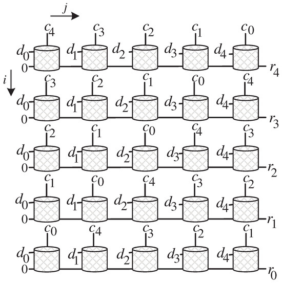
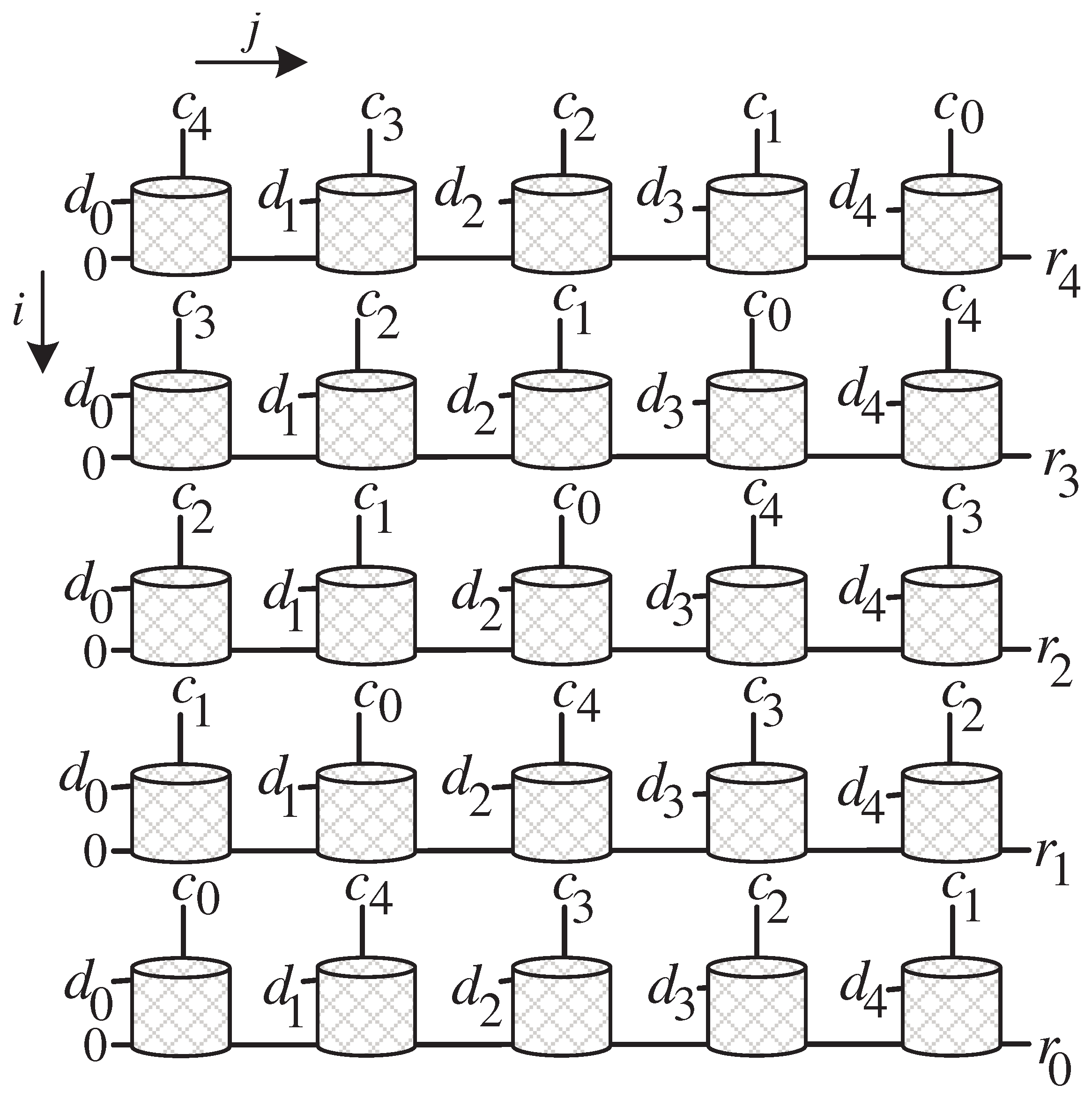
The data dependencies and computational relationships outlined by these expressions are represented in the dependence graph (DG) (for ) shown in Figure 1, which provides a visual mapping of the operations and their interconnections for this modular multiplication process. Based on the extracted dependency graph (DG), the relationship between coefficients follows a systematic flow. The d-coefficients are statically allocated to each node in the graph, while the c-coefficients are provided vertically and cyclically shifted left between rows. This creates a skewed alignment that aligns with the modular polynomial multiplication pattern. The partial results r are initialized to zero and then propagated horizontally across each row.
Figure 1.
DG of the Modular Polynomial Multiplier for .
As the c-coefficients move downward and shift cyclically, each node computes the product of its assigned d-coefficient and the current c-coefficient. The results are accumulated into the pipelined partial result r. This coordinated movement ensures that each term is included in the correct accumulation path for the resulting polynomial coefficient . Moreover, the cyclic shift of c-coefficients automatically implements modular reduction by through sign alternation as the terms wrap around.
4. Development of the Serial Systolic Array
To develop the layout of the bit-serial systolic array, it is essential to meticulously identify the appropriate scheduling and projection vectors for the dependency graph (DG). By following the methodologies presented in earlier studies [23,24,25,26], we can define the scheduling vector, represented as , and the projection vector, represented as , which will effectively assist in designing the serial systolic structure
As demonstrated in [23,26], the scheduling vector is derived from the following scheduling function :
Here, represents the location vector for each node in the dependency graph (DG), while and are the components of the scheduling vector . To ensure that no DG nodes are assigned negative time values, a scalar parameter v is introduced in the previous formula. In this specific case, selecting guarantees that all DG nodes receive positive time assignments.
By analyzing the dependencies among the DG nodes, we can establish the scheduling time allocated to each node , which in turn allows us to determine the components and of the scheduling vector based on Equation (12). While multiple scheduling vectors can be derived from Equation (12), the optimal choice that yields an efficient serial systolic structure is .
Furthermore, as stated in [23,26], the projection vector and the scheduling function must adhere to the following constraint:
With the scheduling vector and the constraints on as specified in Equation (13), there are several possibilities for choosing a projection vector. However, the projection vector that facilitates the construction of the bit-serial systolic array is .
The following projection function must be applied to each DG node to assign the corresponding processing element within the resulting systolic array:
Here, represents a projection matrix. According to [26], the projection vector acts as the null vector of the projection matrix . Given , the corresponding projection matrix should be defined as .
By applying the resulting scheduling vector and the projection matrix to the individual DG nodes , we can derive the associated scheduling function and the projection function , as demonstrated below in Equations (15) and (16). These operations are vital for allocating temporal values to every computational node in the dependency graph, as well as for directing each node to its corresponding processing unit (PE) in the systolic arrangement [23,26]. By combining timing and mapping operations, synchronized and efficient computation management is achieved under a sequentially organized systolic architecture.
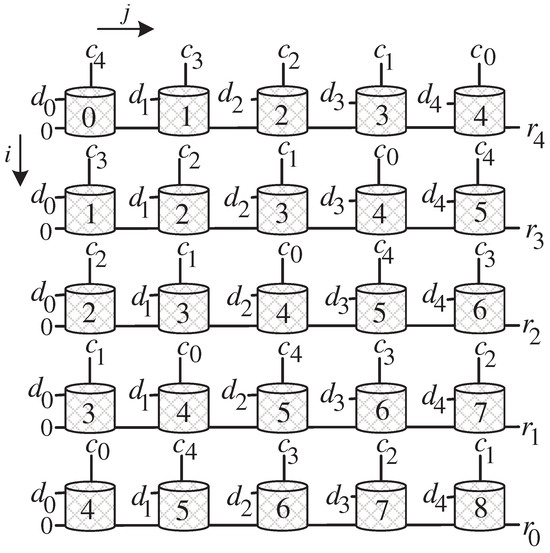
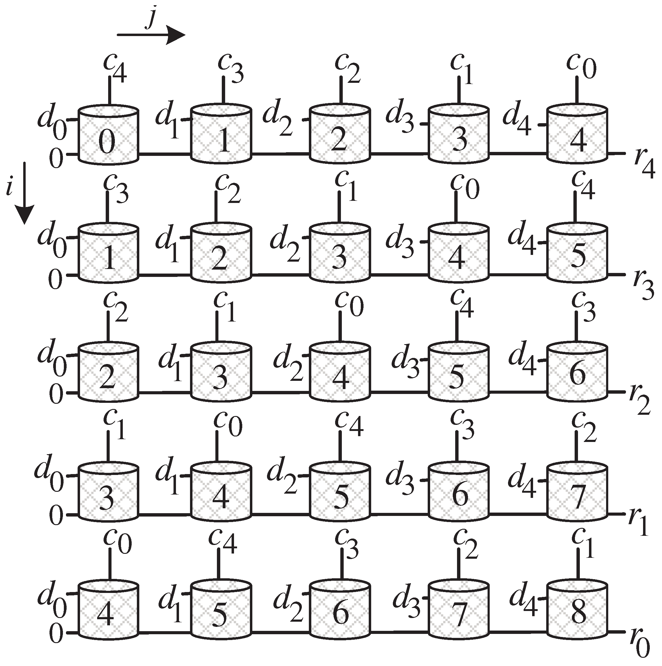
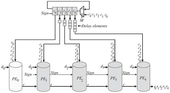
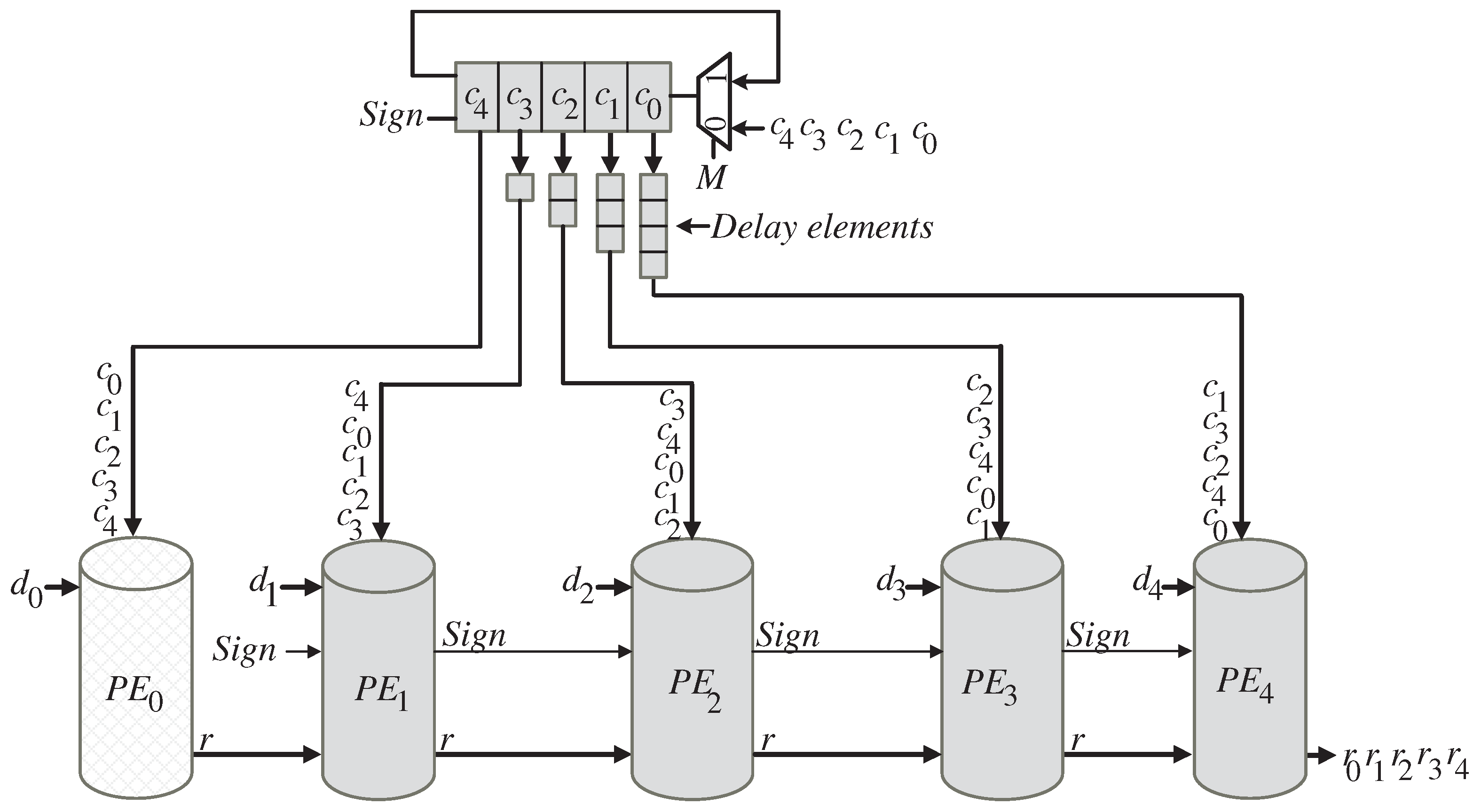
The DG is transformed via the scheduling function , yielding the node timings illustrated in Figure 2. Subsequent application of the projection function to the DG nodes produces the systolic architecture shown in Figure 3. This resulting systolic array is a serial structure comprising l processing elements (PEs), in this example, and completes its computation over a duration of clock cycles (i.e., 9 cycles for ) to generate the final r coefficients serially. Input data is fed serially into the array through the cyclic left shift register (CLSR) and the delay elements (FIFOs) positioned at the top of the structure. As depicted in Figure 3, the coefficient inputs for C from the CLSR are delayed using k-bit FIFOs to ensure their serial availability at the PE inputs. Concurrently, the coefficient bits of operand D are pre-allocated to their respective PEs. Control signals, denoted as , are broadcast to all general-purpose PEs (PEj) to govern the arithmetic operations of addition and subtraction, which will be elaborated upon subsequently. These elements must be arranged in the configuration depicted to ensure proper temporal assignment of each input coefficient c.
Figure 2.
Node Timing of the Developed DG ().
Figure 3.
Suggested serial systolic multiplier for .
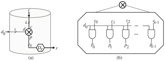
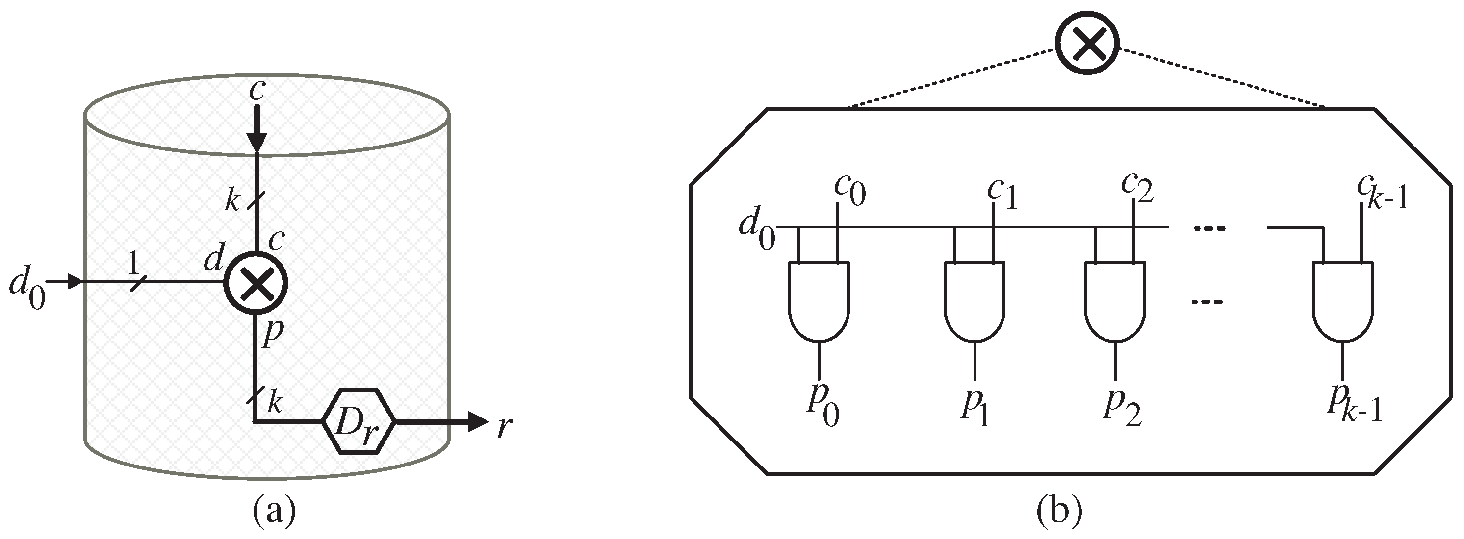
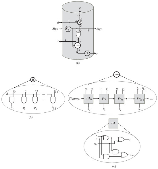
The logical architectures of the first processing element (PE0) and the general processing element (PEj) are detailed in Figure 4 and Figure 5, respectively. PE0, as shown in Figure 4a, possesses a minimal structure consisting solely of a multiplier component and a k-bit register (k Flip-Flops (FFs)), . The internal composition of the multiplier, illustrated in Figure 4b, is an array of k two-input AND gates interconnected as shown. It is important to note that each input coefficient c is a k-bit binary value represented in a 2’s bit representation as .
Figure 4.
(a) Logic circuit of PE0; (b) Details of the adder.
Figure 5.
(a) Logic circuit of the general PE (PEj); (b) Details of the multiplier; (c) Details of the adder.
The general processing element (PEj), depicted in Figure 5a, features a more complex datapath. It integrates a k-bit multiplier, a k-bit adder, an array of k two-input XOR gates, a 1-bit FF (), and a k-bit register (). The subcomponents of the multiplier and adder are shown in Figure 5b and Figure 5c, respectively, with the adder specified as a k-bit ripple-carry adder.
Prior to initiating computation in the serial systolic architecture, a precise initialization sequence must be executed. All FIFOs and FFs within the array must be cleared to establish a known initial state. Furthermore, the control signal for the multiplexer, illustrated in Figure 3, must be set to zero (). This configuration directs the multiplexer to load all coefficients of C into the shift register. Additionally, the signal governs both the cyclic left shift register (CLSR) and the operational mode of processing elements PE1 through PE4 as shown in Figure 3. When activated (), the signal enables the CLSR to circulate left and configures the associated processing elements for addition. Conversely, when deactivated (), it disables the CLSR’s circulation and sets the processing elements to subtraction mode. It should be noted that the signal must remain active () during the first l clock cycles and deactivates () throughout the remaining clock cycles of the computation. This preparatory phase is critical for guaranteeing the reliable and deterministic operation of all subsequent computational steps.
It is important to note that, the input coefficients of C are delivered to their respective processing elements with precisely timed delays. The most significant coefficient ( in our example of ) is connected directly to the first processing element (PE0). The remaining coefficients are fed through a sequence of delay elements: is delayed by one delay element before reaching PE1, is delayed by two delay elements before reaching PE2, is delayed by three delay elements before reaching PE3, and is delayed by four delay elements before reaching PE4. This staggered timing ensures the correct temporal alignment of data for the systolic computation.
The computational procedure for the serial systolic architecture for proceeds as follows:
- At the initial clock cycle, coefficient is presented directly to the first processing element (PE0) to commence computation of the intermediate partial product for . Concurrently, the remaining coefficients are availabe at their respective delay elements.
- At the second clock cycle, control signals and M will be set (, ) to enable the CLSR to be circulate left by one position and make the processing elements from PE1 to PE4 operating in the addition mode. During this time step, coefficient will be available at the input of the first processing element (PE0) to begin computing the intermediate partial product of . Also, during this same time step, the coefficient will propagate through the delay element connected to the second processing element (PE1), and the previously computed partial product from PE0 will be pipelined to PE1 to complete the computation of the intermediate partial product of .
- At the third clock cycle, control signals and M still active (, ) to enable the CLSR to be circulate left by one position. During this time step, coefficient will be available at the input of the first processing element (PE0) to begin computing the intermediate partial product of . Also, during this same time step, the coefficient will propagate through the delay element connected to the second processing element (PE1), and the previously computed partial product from PE0 will be pipelined to PE1 to complete the computation of the intermediate partial product of . Additionally, during this time step, the coefficient also will propagate through the delay elementes connected to the third processing element (PE2), and the previously computed partial product from PE1 will be pipelined to PE2 to complete the computation of the intermediate partial product of .
- At the fourth clock cycle, control signals and M still active (, ) to enable the CLSR to be circulate left by one position. During this time step, coefficient will be available at the input of the first processing element (PE0) to begin computing the intermediate partial product of . Also, during this same time step, the coefficient will propagate through the delay element connected to the second processing element (PE1), and the previously computed partial product from PE0 will be pipelined to PE1 to complete the computation of the intermediate partial product of . Additionally, during this time step, the coefficient will propagate through the delay elementes connected to the third processing element (PE2), and the previously computed partial product from PE1 will be pipelined to PE2 to complete the computation of the intermediate partial product of . Moreover, during this time step, the coefficient will propagate through the delay elementes connected to the fourth processing element (PE3), and the previously computed partial product from PE2 will be pipelined to PE3 to complete the computation of the intermediate partial product of . Note that at this time step the final result of the partial product will be avaialbe at the serial output of the systolic array.
- At the fifth clock cycle, control signals and M still active (, ) to enable the CLSR to be circulate left by one position. During this time step, coefficient will be available at the input of the first processing element (PE0) to begin computing the intermediate partial product of . Also, during this same time step, the coefficient will propagate through the delay element connected to the second processing element (PE1), and the previously computed partial product from PE0 will be pipelined to PE1 to complete the computation of the intermediate partial product of . Additionally, during this time step, the coefficient will propagate through the delay element connected to the third processing element (PE2), and the previously computed partial product from PE1 will be pipelined to PE2 to complete the computation of the intermediate partial product of . Moreover, during this time step, the coefficient will propagate through the delay elementes connected to the fourth processing elementes (PE3), and the previously computed partial product from PE2 will be pipelined to PE3 to complete the computation of the intermediate partial product of . Moreover, during this time step, the coefficient will propagate through the delay elementes connected to the fifth processing element (PE4), and the previously computed partial product from PE3 will be pipelined to PE4 to complete the computation of the intermediate partial product of .
- During the final phase of computation (clock cycles 6 through 9), the signal must remain deactivated (). This configuration halts the cyclic left shift register (CLSR) from circulating and switches all processing elements to subtraction mode.
- At the sixth clock cycle, coefficient becomes available at processing elements PE1 through PE4, enabling computation of intermediate partial results for , , and , while the final result for appears at the serial output.
- At the seventh clock cycle, coefficient reaches processing elements PE2 through PE4, facilitating computation of intermediate partial results for and , with the final result for becoming available at the serial output.
- At the eighth clock cycle, coefficient arrives at processing elements PE3 and PE4, enabling computation of the intermediate partial result for while the final result for emerges at the serial output.
- At the ninth and final clock cycle, coefficient is processed by PE4 to generate the final result for . At this point, all digits of the output coefficients for product R become available on the output bus, completing the computation.
5. Results and Discussions
5.1. Complexity Analysis
The computational complexity of the proposed architecture for computing , under the dual constraints of the ring , is analyzed as follows. The coefficients of the integer polynomial are efficiently loaded into k-bit shift register, known as the CLSR. This shift register has a length of l and uses k two-to-one multiplexers. A set of delay elements, configured as First-In-First-Out (FIFO) buffers, with a total capacity of bits, serially delivers these coefficients to the systolic array, ensuring a smooth and organized flow of data.
The processing elements within the array consist of l parallel k-bit multipliers, implemented using two-input AND gates. This design choice facilitates simultaneous multiplication operations, thus enhancing the overall computational efficiency of the system. The subsequent logic circuits include two-input XOR gates and k-bit ripple carry adders. These adders are crucial for the summation of the partial products and require AND gates, OR gates, and XOR gates to implement the complete addition process accurately. For data storage, the architecture involves flip-flops (FFs) to effectively pipeline the coefficients of the partial product r. An additional flip-flops are implemented to manage the signal, which is essential for determining the operational mode of the circuit.
A key operational feature of this architecture is the connection of the adder input carry to the signal. This configuration permits the circuit to seamlessly perform either addition or subtraction in a two’s complement representation, contingent on the value of the signal, as previously illustrated in the design specifications.
Regarding time complexity, the maximum combinational path delay of the architecture is expressed as , where indicates the propagation delay of a two-input AND gate, and signifies the propagation delay of a two-input XOR gate. The complete computation of the coefficients for necessitates clock cycles, reflecting the architecture’s efficiency and its suitability for high-performance polynomial multiplications within the specified ring constraints. This structured approach ensures that all components work harmoniously to achieve the desired computational goals effectively.
5.2. Implementation and Comparison
To assess the performance efficiency of the proposed architecture, we compare it with several state-of-the-art implementations referenced in [16,17,18,19,20]. The evaluation includes FPGA-based implementation results for the parameter sets and .
To ensure a completely fair and meaningful comparison, a uniform experimental framework was established. Rather than relying on reported figures from various literatures—which may use different synthesis settings or hardware targets—we independently described both the proposed and all competing architectures using the VHDL programming language. This allows for a “like-for-like” evaluation where all designs are implemented on the same Xilinx Kintex-7 AC701 FPGA platform. Furthermore, the entire development process, including synthesis and implementation, was conducted using a consistent toolchain (Vivado 2019.2) under identical clock constraints and optimization strategies. To guarantee functional equivalence and accuracy across all compared models, verification was performed using ModelSim simulation. This methodology ensures that the observed improvements in resource utilization and performance are strictly attributable to our architectural optimizations rather than variations in the implementation environment.
Table 1 provides a comprehensive summary of the implementation results, quantifying the design’s efficiency across area and timing. The results are broken down into several key metrics: the resource utilization, detailed by the consumption of Lookup Tables (LUTs) and Flip-Flops (FF); the maximum achievable clock speed reported as frequency (Fmax, MHz); and the processing latency, given in clock cycles. To offer a holistic view of performance, the table also includes two synthesized figures of merit: the total computational delay (critical-path × latency cycles), which captures the end-to-end processing time, and the Area-Delay Product (ADP) (LUTs × delay), a critical measure of the design’s overall hardware efficiency that balances resource cost against performance speed.
Table 1.
Area-Time Complexity Analysis for Proposed and Alternative designs on the FPGA Platform for and .
Importantly, the delay elements in the proposed architecture are configured as FIFO buffers, which are mapped to Block RAMs (BRAMs). Specifically, for the Artix-7 AC701 FPGA, the proposed systolic design necessitates the use of one BRAM when and three BRAMs when . Each BRAM block in this FPGA is capable of storing 36 kilobits (Kb) of data, which is equivalent to 36,864 bits. Furthermore, a single 6-input Look-Up Table (LUT6) can be configured to function as a -bit Distributed RAM, thus providing a storage capacity of 64 bits. To estimate the equivalent number of LUTs corresponding to one BRAM, one can divide the BRAM storage capacity (36,864 bits) by the LUT storgae capacity (64 bits). This results in an equivalency of 576 LUTs per BRAM. Therefore, in Table 1, we have included the equivalent number of these BRAMs in the total count of LUTs.
The experimental data in Table 1 provide a clear comparison between the proposed hardware design and other existing solutions for two commonly used parameter sets: and . This study shows that the new design consistently achieves a strong balance between resource usage and computational speed. This is best captured by the Area-Delay Product (ADP), which is a measure that combines both hardware area and execution speed to describe overall efficiency.
For , the proposed design demonstrates considerable efficiency. It requires only 8232 look-up tables (LUTs) and 2616 flip-flops (FFs), which is much less than the next-best design, recorded at 9889 LUTs and 3230 FFs. This means the proposed design reduces LUT usage by 16.8% and flip-flop usage by 19%, without sacrificing speed. In fact, the proposed design operates at 280 MHz, which is more than twice the 133 MHz reached by some alternatives. This combination produces an ADP of 15,065, nearly 27% better than the closest competitor, making it a clear leader in hardware efficiency.
When the parameter set increases to , all designs require more resources. Even so, the proposed design keeps its advantage, needing only 17,287 LUTs and 6335 FFs, which is 20.5% and 18.2% fewer LUTs and FFs, respectively, than the second most area-efficient model. The operating frequency remains high at 225 MHz, while other designs only reach between 55 MHz and 111 MHz. The result is an ADP of 78,483, which is 28% better than the nearest rival. These outcomes show that the advantages of the proposed design remain consistent as the computational demands grow.
Overall, the results confirm that this hardware architecture does not focus on a single performance goal. Instead, it finds a smart middle ground between minimizing area and maximizing speed. The design avoids using extra hardware for only small gains in performance and avoids slowing down just to save space. Instead, it keeps an optimal balance, achieving the best ADP in every scenario tested. This design renders the system particularly well-suited for IoT edge modules, where both performance and chip area are essential considerations. The architecture’s ability to sustain high efficiency across varying parameter settings highlights its robustness and enhances its potential impact in practical applications. Building on these findings, the inclusion of the proposed multiplier design into the BRLWE post-quantum scheme will significantly improve its efficiency. This enhancement makes it an ideal candidate for deployment within IoT edge nodes. This advancement not only strengthens the resilience of these devices against post-quantum attacks but also ensures a more secure and reliable infrastructure for the rapidly evolving digital landscape. Furthermore, by addressing the pressing security challenges posed by sophisticated cyber threats, this architecture fosters greater trust and facilitates wider adoption of IoT technologies. In doing so, it aligns seamlessly with the objectives of creating resilient, technology-driven economic activities, thereby contributing to Sustainable Development Goals 8 and 9 and ultimately supporting the development of a more secure and productive digital economy. This fusion of enhanced security and efficiency underscores the architecture’s pivotal role in advancing the future of IoT applications.
6. Summary and Conclusions
The rapid proliferation of IoT devices necessitates robust security solutions, particularly in the context of emerging quantum threats. We have focused on optimizing polynomial multiplication, a fundamental operation in lattice-based post-quantum cryptographic schemes, specifically within the BRLWE scheme framework. The proposed low-complexity serial systolic array architecture has demonstrated significant performance enhancements, achieving a maximum operating frequency while maintaining an efficient resource footprint with reduced lookup tables and flip-flops. These improvements correspond to a substantial reduction in resource utilization compared to existing designs, ensuring high throughput and minimal area consumption. This design effectively addresses the critical needs of IoT edge nodes, enhancing their resilience against post-quantum attacks and supporting the establishment of a secure and efficient infrastructure for digital economic activities. Moreover, it aligns with Sustainable Development Goals 8 and 9 by fostering trust and facilitating the integration of advanced IoT technologies. In conclusion, our architecture not only advances the state of the art in post-quantum cryptography but also provides a pathway for the broader adoption of secure IoT systems. Future work could include integrating the proposed systolic multiplier into the BRLWE scheme to demonstrate its performance and area improvements, as well as analyzing the resistance of the design against side-channel attacks. By continuing to refine and enhance our multipliers and cryptographic protocols, we aim to support a transformative and secure digital economy that thrives on innovation and resilience.
Author Contributions
Conceptualization, A.I.; methodology, A.I. and F.G.; software, A.I.; validation, A.I.; formal analysis, A.I.; investigation, A.I.; resources, A.I.; data curation, A.I.; writing—original draft preparation, A.I.; writing—review and editing, A.I. and F.G.; visualization, A.I.; supervision, A.I.; project administration, A.I.; funding acquisition, A.I. All authors have read and agreed to the published version of the manuscript.
Funding
This research was funded by Prince Sattam bin Abdulaziz University through project number (PSAU/2025/01/34935).
Institutional Review Board Statement
Not applicable.
Informed Consent Statement
Not applicable.
Data Availability Statement
The original contributions presented in this study are included in the article.
Acknowledgments
The authors extend their appreciation to Prince Sattam bin Abdulaziz University for funding this research work through the project number (PSAU/2025/01/34935).
Conflicts of Interest
The authors declare no conflict of interest.
Abbreviations
The following abbreviations are used in this manuscript:
| IoT | Internet of Things |
| PQC | Post Quantum Cryptography |
| NIST | National Institute of Standard |
| SVP | Shortest Vector Problem |
| LWE | Learning With Errors |
| BRLWE | Binary Ring Learning With Errors |
| PB | Polynomial Basis |
| VLSI | Very Large Scale Integrated Circuit |
| FPGA | Field Programmable Gate Array |
| RSA | Rivest, Shamir, and Adleman |
| ECC | Elliptic Curve Cryptography |
| DG | Dependency Graph |
| PE | Processing Element |
| FIFO | First Input First Output |
| CLSR | cyclic Left Shift Register |
| LUT | Lookup Table |
| ADP | Area-Delay Product |
| FFs | Flip-Flops |
References
- Magara, T.; Zhou, Y. Internet of things (IoT) of smart homes: Privacy and security. J. Electr. Comput. Eng. 2024, 2024, 7716956. [Google Scholar] [CrossRef] [Scilit]
- Diop, M.; Ndiaye, P.; Dione, D.; Diop, I. IoT Security in the Quantum Era: State of the Art and Open Challenges. In Proceedings of the 2025 5th International Conference on Innovative Research in Applied Science, Engineering and Technology (IRASET), Fez, Morocco, 15–16 May 2025; IEEE: New York, NY, USA, 2025; pp. 1–11. [Google Scholar]
- Ebrahimi, S.; Bayat-Sarmadi, S.; Mosanaei-Boorani, H. Post-quantum cryptoprocessors optimized for edge and resource-constrained devices in IoT. IEEE Internet Things J. 2019, 6, 5500–5507. [Google Scholar] [CrossRef] [Scilit]
- Rathod, P.; Bhatt, N.; Nema, R.; Jyotheeswari, P. A Comprehensive Review on IoT Security Challenges and Solutions. In Proceedings of the 2025 Seventh International Conference on Computational Intelligence and Communication Technologies (CCICT), Sonepat, India, 11–12 April 2025; IEEE: New York, NY, USA, 2025; pp. 696–701. [Google Scholar]
- Wang, X.B.; Yu, Z.W.; Hu, X.L. Twin-field quantum key distribution with large misalignment error. Phys. Rev. A 2018, 98, 062323. [Google Scholar] [CrossRef] [Scilit]
- Regev, O. On lattices, learning with errors, random linear codes, and cryptography. J. ACM 2009, 56, 1–40. [Google Scholar] [CrossRef] [Scilit]
- Buchmann, J.; Göpfert, F.; Player, R.; Wunderer, T. On the hardness of LWE with binary error: Revisiting the hybrid lattice-reduction and meet-in-the-middle attack. In Proceedings of the International Conference on Cryptology in Africa, Fes, Morocco, 13–15 April 2016; Springer: Cham, Switzerland, 2016; pp. 24–43. [Google Scholar]
- Asif, R. Post-quantum cryptosystems for Internet-of-Things: A survey on lattice-based algorithms. IoT 2021, 2, 71–91. [Google Scholar] [CrossRef] [Scilit]
- Dam, D.T.; Tran, T.H.; Hoang, V.P.; Pham, C.K.; Hoang, T.T. A survey of post-quantum cryptography: Start of a new race. Cryptography 2023, 7, 40. [Google Scholar] [CrossRef] [Scilit]
- Chen, C.; Danba, O.; Hoffstein, J.; Hülsing, A.; Rijneveld, J.; Schanck, J.M.; Schwabe, P.; Whyte, W.; Zhang, Z. Algorithm Specifications and Supporting Documentation; Brown University: Wilmington, NC, USA; Onboard Security Company: Wilmington, NC, USA, 2019. [Google Scholar]
- Bos, J.; Ducas, L.; Kiltz, E.; Lepoint, T.; Lyubashevsky, V.; Schanck, J.M.; Schwabe, P.; Seiler, G.; Stehlé, D. CRYSTALS-Kyber: A CCA-secure module-lattice-based KEM. In Proceedings of the 2018 IEEE European Symposium on Security and Privacy (EuroS&P), London, UK, 24–26 April 2018; IEEE: New York, NY, USA 2018; pp. 353–367. [Google Scholar]
- D’Anvers, J.P.; Karmakar, A.; Sinha Roy, S.; Vercauteren, F. Saber: Module-LWR based key exchange, CPA-secure encryption and CCA-secure KEM. In Proceedings of the International Conference on Cryptology in Africa, Marrakesh, Morocco, 7–8 May 2018; Springer: Cham, Switzerland, 2018; pp. 282–305. [Google Scholar]
- Buchmann, J.; Göpfert, F.; Güneysu, T.; Oder, T.; Pöppelmann, T. High-performance and lightweight lattice-based public-key encryption. In Proceedings of the 2nd ACM International Workshop on IoT Privacy, Trust, and Security, Xi’an, China, 30 May 2016; pp. 2–9. [Google Scholar]
- He, P.; Guin, U.; Xie, J. Novel low-complexity polynomial multiplication over hybrid fields for efficient implementation of binary ring-LWE post-quantum cryptography. IEEE J. Emerg. Sel. Top. Circuits Syst. 2021, 11, 383–394. [Google Scholar] [CrossRef] [Scilit]
- Basso, A.; Bos, J.W.; D’Anvers, J.P.; Karmakar, A.; Mera, J.M.B.; Renes, J.; Roy, S.S.; Vercauteren, F.; Wang, P.; Wang, Y.; et al. Using Learning with Rounding to Instantiate Post-Quantum Cryptographic Algorithms. Cryptol. ePrint Arch. 2025. Available online: https://eprint.iacr.org/2025/1382 (accessed on 26 February 2026).
- Bao, T.; He, P.; Xie, J. Systolic acceleration of polynomial multiplication for KEM saber and binary ring-LWE post-quantum cryptography. In Proceedings of the 2022 IEEE International Symposium on Hardware Oriented Security and Trust (HOST), McLean, VA, USA, 27–30 June 2022; IEEE: New York, NY, USA, 2022; pp. 157–160. [Google Scholar]
- Xie, J.; He, P.; Wen, W. Efficient implementation of finite field arithmetic for binary ring-LWE post-quantum cryptography through a novel lookup-table-like method. In Proceedings of the 2021 58th ACM/IEEE Design Automation Conference (DAC), San Francisco, CA, USA, 5–9 December 2021; IEEE: New York, NY, USA, 2021; pp. 1279–1284. [Google Scholar]
- Tan, W.; Wang, A.; Zhang, X.; Lao, Y.; Parhi, K.K. High-speed VLSI architectures for modular polynomial multiplication via fast filtering and applications to lattice-based cryptography. IEEE Trans. Comput. 2023, 72, 2454–2466. [Google Scholar] [CrossRef] [Scilit]
- Roy, S.S.; Basso, A. High-speed instruction-set coprocessor for lattice-based key encapsulation mechanism: Saber in hardware. IACR Trans. Cryptogr. Hardw. Embed. Syst. 2020, 2020, 443–466. [Google Scholar]
- Basso, A.; Roy, S.S. Optimized polynomial multiplier architectures for post-quantum KEM saber. In Proceedings of the 2021 58th ACM/IEEE Design Automation Conference (DAC), San Francisco, CA, USA, 5–9 December 2021; IEEE: New York, NY, USA, 2021; pp. 1285–1290. [Google Scholar]
- Ebrahimi, S.; Bayat-Sarmadi, S. Lightweight and fault-resilient implementations of binary ring-LWE for IoT devices. IEEE Internet Things J. 2020, 7, 6970–6978. [Google Scholar] [CrossRef] [Scilit]
- Imaña, J.L.; He, P.; Bao, T.; Tu, Y.; Xie, J. Efficient hardware arithmetic for inverted binary ring-lwe based post-quantum cryptography. IEEE Trans. Circuits Syst. I Regul. Pap. 2022, 69, 3297–3307. [Google Scholar] [CrossRef] [Scilit]
- Ibrahim, A. Efficient parallel and serial systolic structures for multiplication and squaring over gf(2m). Can. J. Electr. Comput. Eng. 2019, 42, 114–120. [Google Scholar] [CrossRef] [Scilit]
- Ibrahim, A.; Gebali, F. Enhancing Security and Efficiency in IoT Assistive Technologies: A Novel Hybrid Systolic Array Multiplier for Cryptographic Algorithms. Appl. Sci. 2025, 15, 2660. [Google Scholar] [CrossRef] [Scilit]
- Ibrahim, A.; Gebali, F. Optimizing Security of Radio Frequency Identification Systems in Assistive Devices: A Novel Unidirectional Systolic Design for Dickson-Based Field Multiplier. Systems 2025, 13, 154. [Google Scholar] [CrossRef] [Scilit]
- Gebali, F. Algorithms and Parallel Computers; John Wiley: New York, NY, USA, 2011. [Google Scholar]

Disclaimer/Publisher’s Note: The statements, opinions and data contained in all publications are solely those of the individual author(s) and contributor(s) and not of MDPI and/or the editor(s). MDPI and/or the editor(s) disclaim responsibility for any injury to people or property resulting from any ideas, methods, instructions or products referred to in the content. |
© 2026 by the authors. Licensee MDPI, Basel, Switzerland. This article is an open access article distributed under the terms and conditions of the Creative Commons Attribution (CC BY) license.