Abstract
This study introduces a novel approach for analyzing thin film interference spectra by employing a micro-spectrometer equipped with a spectral chip. Focusing on zinc oxide (ZnO) thin films prepared via the sol–gel method, this research aims to explore the films’ physical properties through spectral analysis. After obtaining the interference spectrum of the ZnO thin films, the peak positions within the spectrum were cataloged. Mathematical simulation was used to adjust the refractive index and thickness of the films to match the simulated interference peak positions with the observed peak positions. The thickness of the prepared ZnO film was estimated to be 4.9 μm and its refractive index at 80 °C was estimated to be 1.96. In addition, the measurement system was used to detect environmental changes, including temperature changes and gas exposure. It was observed that the optical characteristics of ZnO films exhibit marked variations with temperature shifts, enabling the establishment of a temperature calibration curve based on spectral feature displacement. In addition, experiments using a variety of gases showed that NO2 and gaseous isopropanol significantly affect the interference spectrum of ZnO, with the peak of the interference spectrum shifted by 2.3 nm and 5.2 nm, respectively, after injection of the two gases. This indicates that interferometric spectroscopy can serve as an effective tool for ZnO monitoring, capable of selectively detecting specific gases.
1. Introduction
Thin film technology focuses on the fabrication and application of ultra-thin layers of solid-state materials, playing an indispensable multifunctional role in the field of materials science [1]. The thickness of these films typically ranges from several nanometers to a few micrometers, endowing them with unique physical and chemical properties that have a significant impact across various domains, from electronics to energy, and from biomedicine to optics [2,3]. The value of thin film technology lies not only in its miniature scale but also in its ability to finely control physical and chemical properties such as light, electricity, and heat. For example, their optical properties can be easily customized to selectively reflect, absorb, or transmit light of different wavelengths [4]. This feature has led to their widespread use in manufacturing anti-reflective coatings for glasses and solar panels, improving efficiency by reducing glare and increasing energy capture [5].
Despite the wide-ranging applications and promising advantages of thin films, their fabrication and integration into functional systems still pose technical challenges. Common thin film manufacturing techniques include physical vapor deposition (PVD), chemical vapor deposition (CVD), spin coating, and sputter deposition [2,6,7]. The characteristics of thin films are closely related to their thickness and uniformity; therefore, precise thickness control is essential regardless of the production method used. Moreover, ensuring the durability, adhesion, and compatibility of thin films with substrates remains a key factor for their long-term application and performance. Currently, the evaluation of thin films often involves destructive processes, resulting in irreversible alterations that render the samples unsuitable for further analysis [8]. Consequently, the quest for non-destructive detection techniques has steered researchers towards exploring optical methods of materials analysis, which have demonstrated significant promise [9,10].
Utilizing the optical properties of thin films for process monitoring represents an efficient, accurate, non-invasive detection method that can instantaneously reflect changes in key parameters during the film production process [11]. The optical properties of thin films, such as reflectivity, transmittance, and absorbance, are highly sensitive to factors like material thickness, composition, and surface roughness. By accurate optical measurement, real-time monitoring of the thin film manufacturing process can be achieved, allowing for the timely detection of changes in film uniformity, thickness, and other important physical and chemical characteristics [11,12].
Ellipsometers are widely used as rigorous optical instruments for precise measurement of thin film characteristics [13]. However, this method of measurement is not only time-consuming and labor-intensive but also costly. Fortunately, with the advancement of micro-electro-mechanical systems (MEMS) technology, many optical components have been miniaturized and can be integrated onto a single chip [14,15]. Notably, the progress in micro-spectrometer technology has transformed some of the traditional, cumbersome detection equipment into compact, portable devices suitable for point-of-care testing (POCT) applications [16,17]. For instance, Ko et al. effectively employed micro-spectrometers for biochemical/optical detection, pioneering various POCT devices [17,18]. This application of micro-spectrometers in thin film optics analysis, with potential extensions to environmental monitoring, presents a practical and promising approach.
This study evaluates the performance of a designed system using zinc oxide (ZnO) thin films to measure interference spectra. ZnO was chosen because it is easy to prepare, sensitive to gases, has a quick response, and maintains chemical stability [19,20,21]. ZnO thin films, synthesized through cost-effective techniques like sol–gel, spray pyrolysis, and chemical vapor deposition, offer precise control over their thickness and morphology. They are highly sensitive to gases such as NO2, SO2, and ethanol due to their large surface area, adaptable surface properties, and surface defects, allowing for enhanced gas interactions [19]. ZnO’s rapid response to changes in gas concentrations is crucial for real-time monitoring and detection, enabled by swift changes in electrical resistance when exposed to different gases [21]. Additionally, ZnO thin films demonstrate excellent chemical stability, ensuring consistent performance over time, which is crucial for long-term use.
Building upon these technological advancements, this study aims to combine micro-spectrometer technology with thin film detection methods, developing a portable thin film sensing technology. Such portable technology facilitates real-time monitoring and continuous long-term measurements, enhancing the quality of industrial production and furthering scientific research.
2. Materials and Methods
2.1. Thin Film Preparation
In this research, zinc oxide thin films were produced via the sol–gel technique, marking a significant advancement over traditional vacuum sputtering methods [22,23]. This innovative process incorporates spin-coating deposition technology, enabling the creation of oxide thin films under ambient temperature and pressure conditions. This approach notably lowers both the production costs and the time required for processing [24,25]. Furthermore, given the study’s reliance on an optical inspection method, there is a deliberate effort to increase the thickness of the film. This strategy aimed to maximize the difference in the optical path of the interfering lights, ensuring an optimal range for precise measurement.
The preparation process began with the homogeneous mixing of 1 g of zinc acetate [Zn(CH3COO)2·2H2O], 0.15 mL of ethanolamine [C2H7NO], and 20 mL of ethylene glycol monomethyl ether [CH2OHCH2OCH3] using magnetic stirring. The mixture was then heated to 80 degrees Celsius on a hot plate and reacted for 8 h to obtain a stable colloidal solution. Subsequently, the ZnO colloidal solution was uniformly coated onto a silicon substrate using spin-coating technology, forming the thin film. After the coating was completed, the substrate was placed on a hot plate and baked for 15 min at 180 degrees Celsius under normal atmospheric conditions to ensure film integrity and stability.
2.2. Micro-Spectrometer Specificition
This research employed a micro-spectrometer developed by Ko et al., which consolidates various optical structures onto a singular chip [26,27]. Figure 1 illustrates the optical chip’s architecture and its critical microstructures, captured via scanning electron microscopy (SEM). Unlike traditional spectrometers, this optical chip successfully integrates essential optical structures onto a single chip, significantly reducing the overall size of the optical system. Despite its reduced size, this advanced spectral chip is still able to cover the spectral range from 350 nm to 930 nm with a resolution of 5 nm (full width at half maximum, FWHM), maintaining a high optical resolution. Table 1 provides a comprehensive overview of the miniature spectrometer’s specifications.
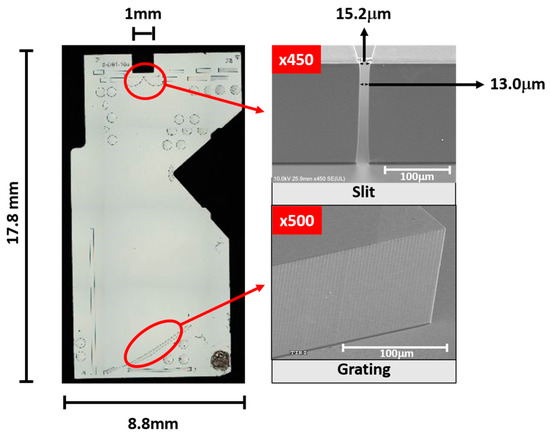
Figure 1.
Optical chip (full view) and critical spectral spectroscopic structure (SEM photo); the slit shown in the upper red circle is the entrance of the incident light into the system; the grating shown in the lower red circle is used for spectral dispersion of the incident light.

Table 1.
Optical specifications of the micro-spectrometer.
Additionally, Figure 2 displays the spectral results of a standard mercury-argon light source conducted with this spectrometer. The spectrometer’s miniaturization not only dramatically decreases the optical system’s size but also offers versatility for a wide array of spectral analyses across different settings.
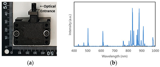
Figure 2.
(a) The compact dimensions of the micro-spectrometer engineered through optical MEMS technology; (b) the measurement results obtained using a standard light source (Hg-Ar lamp), demonstrating an optical resolution of 5 nm and producing results that rival those from traditional, larger spectrometers.
2.3. Optical System Setup
2.3.1. Optical Interference Principle
This research aimed to monitor the state of thin films by observing optical interference phenomena on their surfaces. The wave properties of light lead to the formation of constructive and destructive interference patterns. Thin films ranging from several nanometers to a few micrometers in thickness provide an ideal environment for observing optical phenomena. When light encounters a thin film, part of the light wave is reflected off the surface, while another part penetrates the film and reflects off the bottom surface. These two parts of the light wave—reflected from the top and bottom surfaces—either reinforce or cancel each other out upon leaving the film, depending on their relative phase differences [28,29].
Figure 3 shows a schematic diagram of optical interference phenomena on the surface of a thin film, explaining the optical path and the conditions that lead to constructive or destructive interference. These conditions include the wavelength of light, the thickness of the film, the angle of incident light, and the refractive index of the material of interest.
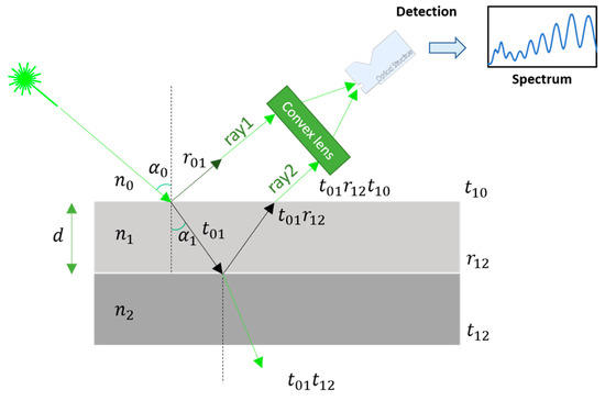
Figure 3.
The schematic representation of the path of light due to interference phenomena on thin film surfaces is characterized by several parameters: n represents the refractive index, d denotes the thickness of the film, α signifies the angle of incidence or refraction, r corresponds to the material’s reflection, and t represents the material’s transmission coefficients.
Based on Figure 3, we can derive the interference spectral model of the thin film surface. The intensity of light (IR) is directly proportional to the square of the amplitude of the light wave (A):
Ray 1 and ray 2, respectively, represent the two light waves reflected at the surface of the thin film and at the surface of the substrate. The complex amplitude resulting from their superposition can be expressed as follows:
In Equation (2), r denotes the reflectance, t is the transmittance, and the subscript 12 indicates the transition from material 1 to material 2. Furthermore, δ represents the phase difference between ray 1 and ray 2, which can be calculated through the optical path length difference between the two rays ():
In Equation (3), d stands for the film’s thickness, λ represents the wavelength of the incident light source, and n is the refractive index of the material. The interference spectrum of thin films is typically obtained using a broadband light source. At different wavelengths, variations in optical path lengths result in either constructive or destructive interference. By analyzing these interference patterns across various wavelengths using a spectrometer, we can deduce the condition of the film. Notably, phase reversal happens when light transitions from a medium with a lower refractive index to one with a higher index. In our research, the refractive index of the atmosphere is approximately 1, that of ZnO ranges from 1.8 to 2, and that of Si is around 3.4. As a consequence, light ray 1 experiences a phase reversal upon reflecting off the film’s surface, and light ray 2 undergoes a phase reversal at the film–substrate interface. Thus, in these scenarios, it is essential to consider only the phase differences arising from the differences in optical path lengths.
Subsequently, we can employ the following relationships between reflection (rij) and transmission coefficients (tij) to calculate the amplitude intensity of the interfering light as delineated in Equation (2):
The superposition result of ray 1 and ray 2 can be rewritten as follows:
where the refractive angle () can be estimated through the incident angle () and the refractive index of the material (n1, n2) using Snell’s law:
Through Equation (6), optical interference phenomena can be simulated under the condition of ignoring polarized light. Moreover, given the minimal absorption by ZnO and the study’s concentration on the shift in interference peaks over actual changes in light intensity, the simulation emphasizes the alterations in interference patterns rather than the impact of film absorption [30]. Unlike ellipsometers, which demand precise incident angle adjustments to deduce thin film properties, this study’s system concentrates on the practical applications of interference spectroscopy. Consequently, the incident angle is set at 0 degrees, effectively reducing the influence of polarized light to an insignificant extent.
2.3.2. Optical Measurement System Setup
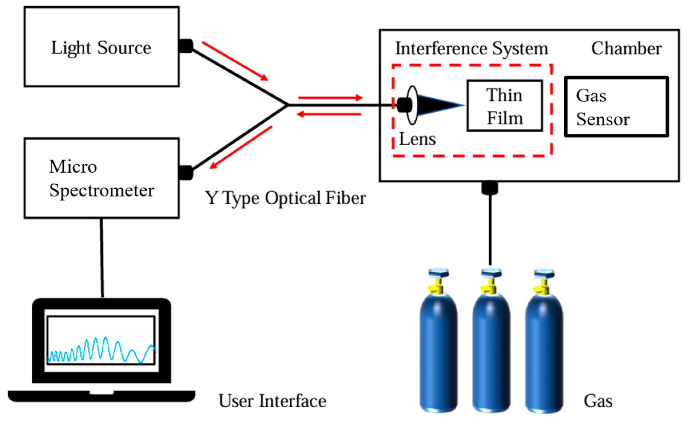
This research was carried out in partnership with the Taiwan Instrument Research Institute (TIRI), making use of their comprehensive gas measurement platform. By employing a gas chamber with precise environmental control, we investigated the performance of our thin film interference spectroscopy measurement system. The structural arrangement of the system is illustrated in Figure 4, demonstrating how its components are integrated for enhanced efficiency. Within this setup, a Y-shaped optical fiber—a frequently used optical component —is deployed to channel light from the source to the thin film’s surface and to relay the reflected interference light back to the micro-spectrometer for subsequent analysis.

Figure 4.
The diagram of a thin film interference spectrum measurement system.
In this study, a deuterium-halogen lamp serves as the light source, spanning a wavelength range from ultraviolet (UV) to near-infrared (NIR). This broad spectrum is pivotal, as per the principles of optical interference, enabling the detection of a wide array of interference phenomena [31]. Such capability significantly enhances our spectral analysis, providing in-depth insight into the thin film’s optical attributes. Additionally, a standard gas sensor is integrated into the chamber setup, positioned alongside the thin film and optical fiber. This sensor serves as a control, offering ongoing insights into the chamber’s environmental conditions. The ability to link alterations in the interference spectrum with live environmental data allows us to identify the nuanced impacts of atmospheric changes on the thin film’s properties. Furthermore, an automated UI interface, developed with LabVIEW, manages the micro-spectrometer operations and facilitates the processing of data in real-time.
3. Results and Discussion
3.1. Characterization of ZnO Thin Films
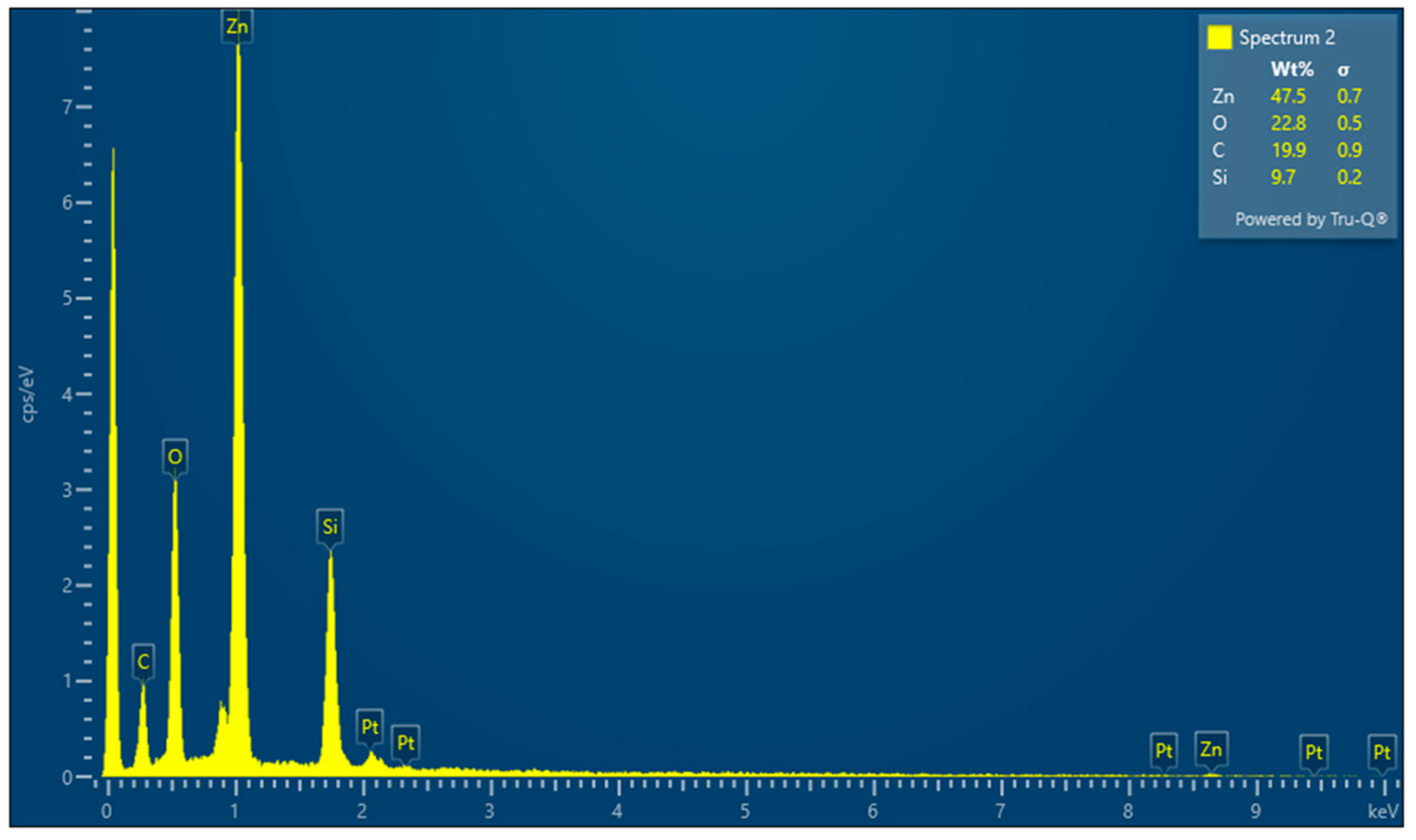
Upon completion of the fabrication process, the microstructure of the thin films was meticulously analyzed using a scanning electron microscope (SEM) to evaluate their surface morphology and crystal quality, as detailed in Figure 5. Considering that the optical properties of the films are primarily determined by their thickness, this study precisely controlled the thickness of the ZnO thin films by adjusting the spin-coating parameters [22,23,32]. After the preparation of the ZnO thin films, energy dispersive spectroscopy (EDS) was employed for elemental distribution analysis. Figure 6 presents the EDS analysis images of the ZnO thin film, revealing the distribution states of Si, zinc (Zn), and oxygen (O) elements on the sample. Figure 7 shows the results of elemental mapping using EDS, indicating that the film comprises 32.5% silicon (Si), 30% Zn, and 17.4% O. EDS and SEM measurements are provided in the Supplementary Materials section.
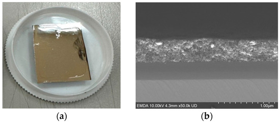
Figure 5.
(a) ZnO thin films prepared using the sol–gel method; (b) scanning electron microscopy cross-sectional image of ZnO thin film.
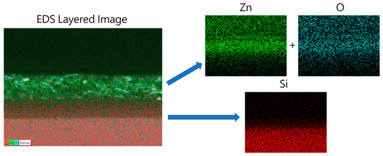
Figure 6.
EDS elemental mapping results delineate the spatial distribution of different elements, each represented by distinct colors.

Figure 7.
The EDS elemental mapping results that determine the concentration of each element.
3.2. Interference Spectroscopy of ZnO
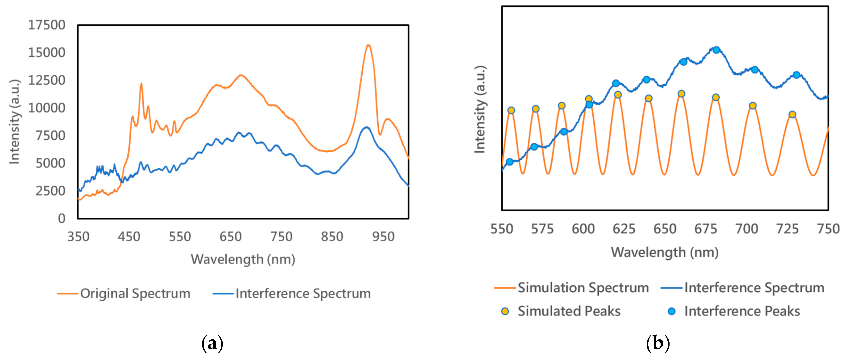
The blue line in Figure 8a illustrates the interference spectrum of the ZnO thin film, revealing roughly a dozen distinct wave peaks between 550 and 750 nm. Meanwhile, the red line in the same figure displays the raw spectrum from the deuterium-halogen lamp, showcasing a comparatively uniform intensity distribution within this range and clearly highlighting the interference effect. In the ultraviolet and near-infrared bands, despite the presence of interference phenomena, the intensity distribution is inherently uneven. Additionally, the sensitivity of our chosen instruments, such as spectrometers and optical fibers, is lower in these bands, complicating observations.
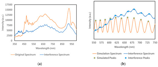
Figure 8.
(a) The blue line is the original deuterium spectrum and the red line is the interference spectrum reflected by ZnO thin film. By comparing the two spectra, we can clearly observe a significant interference pattern in the range of 550 to 750 nm, which can serve as a reference for simulation calculations; (b) Comparing the difference in the peak positions between the numerically simulated interferometric reflectance spectra of the films and the actual interferometric spectra, and then predicting the physical properties of the films by tuning n1 and d.
Consequently, our study’s spectral analysis primarily concentrated on the 550–750 nm range. Before beginning the interference spectral analysis, we processed the interference spectrum by first subtracting the dark spectral intensity, then normalized the full spectral range, and finally extracted the target band (550–750 nm) for subsequent analysis.
By analyzing the wavelengths of these peak positions, simulation parameters can be adjusted for fitting, allowing for the calculation of changes in the film’s refractive index (n1) or thickness, as illustrated in Figure 8b. In this study, n0 and n2 are constants (with n0, the refractive index of air, being 1, and n2, the refractive index of silicon, derived from the data provided by Schinke et al.), and the angle of incidence is consistently set to 0 degrees [33]. Therefore, the primary variables for fitting the interference spectrum are n1 (the refractive index of ZnO) and d (the thickness of the ZnO layer). This section of the simulation process begins by identifying the peak position of the interference wave (wavelength) within the interference spectrum, specifically in the 550–750 nm range. The film thickness (d) was initially determined from scanning electron microscope observations and later adjusted through comparisons with the actual interference spectrum. Notably, an increase in film thickness leads to a higher count of interference peaks within the observed spectral range. Subsequently, the refractive index n1 is adjusted. As the value of n1 changes, the peaks of simulated interference shift towards either lower or higher wavelengths. To refine the simulation’s accuracy, the mean absolute error (MAE) between the peaks in the simulated spectrum and those in the actual interference spectrum is calculated. The goal is to minimize the MAE value as much as possible, thereby enhancing the precision of the simulation. Table 2 presents the results of the interference spectrum fitting, with the MAE of the bias from the actual spectral peak closely matching the spectrometer’s measurement error (2 × 0.375 nm). We added two flow charts in the Supplementary Materials section that illustrate the process of sampling the spectral data and simulating the fit. Additionally, two flow charts in the Supplementary Materials section explain the process of sampling spectral data and simulating the fitting process.

Table 2.
MAE evaluation results at 80 °C.
3.3. Environmental Monitoring
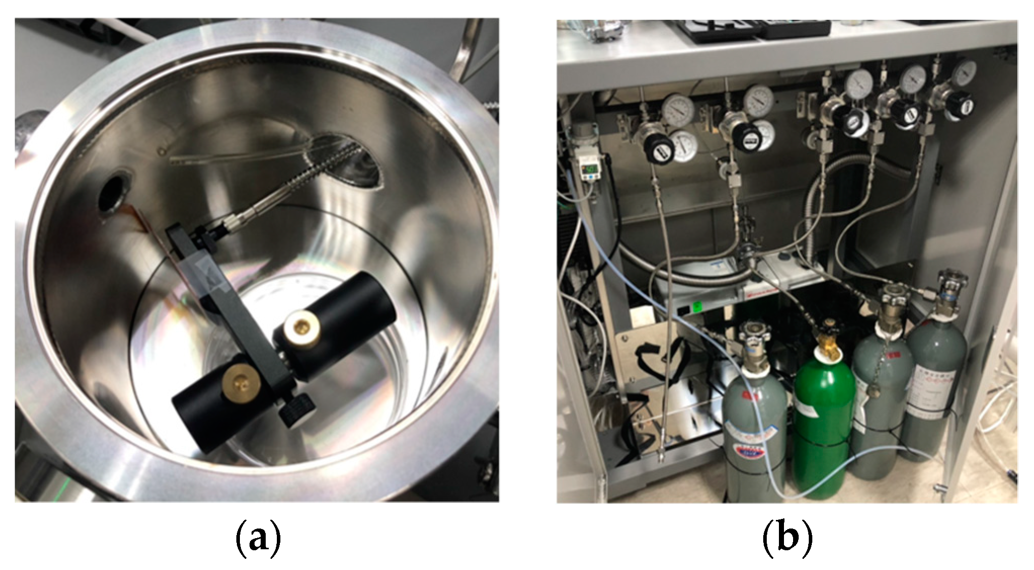
TIRI provides a standard gas measurement environment, enabling this study to validate the environmental sensing capabilities of thin films. Figure 9a shows the actual enclosed gas chamber environment used for testing, employing a Y-shaped optical fiber with flanges, which achieves bidirectional light communication and effectively maintains the chamber’s seal, ensuring that the gas is evenly distributed within the chamber. Figure 9b demonstrates the gas introduction device provided by TIRI for testing, which allows users to introduce test gas into the chamber by controlling the gas valve.

Figure 9.
(a) The optical path setup within the gas chamber; (b) the gas valve control system of ITRI.
3.3.1. Temperature
Thin films are sensitive to environmental changes, with temperature being one of the key environmental factors [34,35]. Variations in temperature can affect the optical transparency and bandgap of zinc oxide films. As the temperature increases, the transparency of the film may improve, but excessively high temperatures may lead to defects, such as an increase in oxygen vacancies, thereby affecting its optical performance [21,32]. The bandgap may also vary with an increase in grain size and an improvement in crystallinity [32].
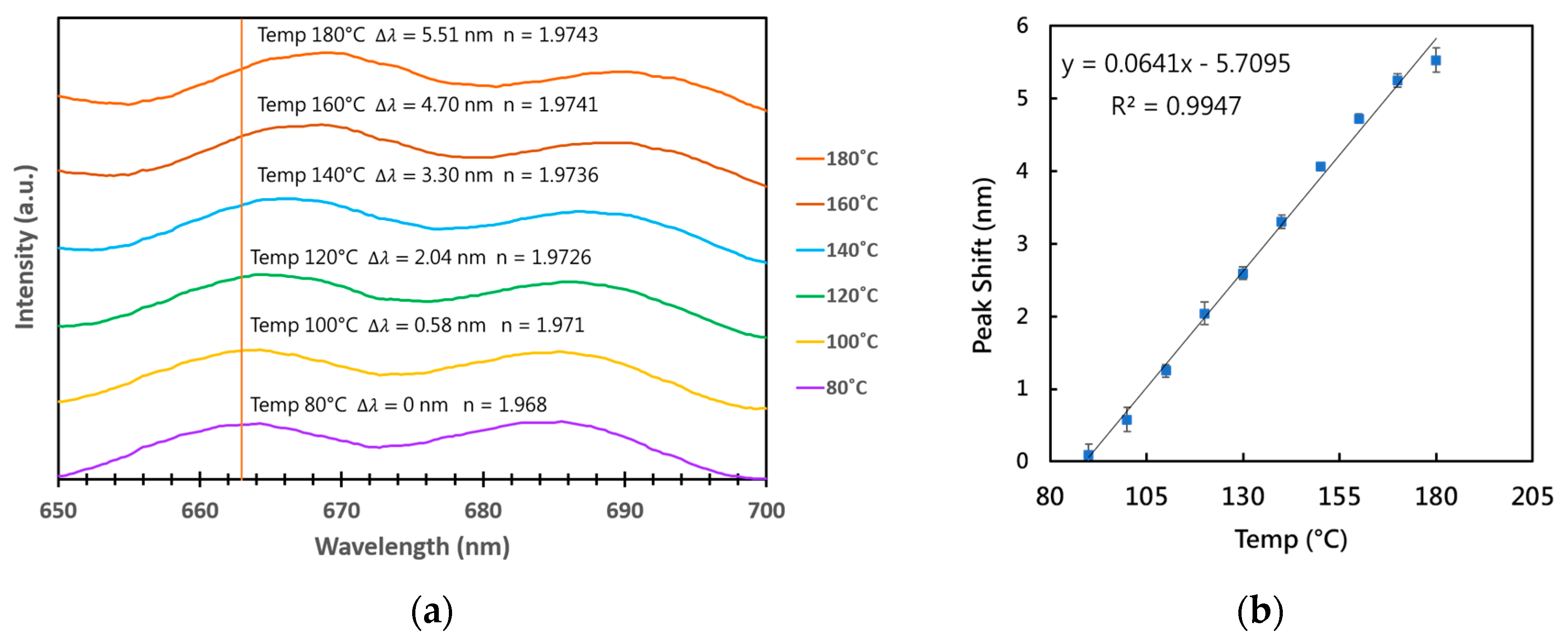
To ascertain the actual impact of environmental temperature on ZnO, this study utilized a heating plate to adjust the temperature of the thin film while measuring its interference spectra. The interference spectra at six different temperatures are presented in Figure 10a. As the temperature increases, the peaks and valleys of the interference spectrum shift towards lower wavelengths. Using the evaluation method mentioned in Section 3.2, we adjusted the parameters n1 and d in the simulation to minimize the MAE and to simulate the current film state. The displacement of the interference spectra’s peak at various temperatures was quantified, using the spectrum at 80 °C as a reference, and is marked as Δλ in Figure 10a. Subsequently, for simulation within the 550–750 nm spectral region, the method outlined in Section 3.2 was employed. In this simulation, the parameters n1 and d were adjusted to minimize the MAE, thereby closely replicating the state of the film under current conditions. The estimated value of n1, obtained through simulation, is also depicted in Figure 10a, illustrating that n1 increases with temperature, leading to a shift in the peak of the interference spectra.
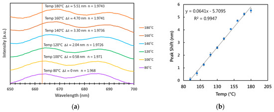
Figure 10.
(a) The ZnO interference spectra at six different temperatures, with adjustments made to the Y-axis of the interference spectra for easier identification of spectral shifts by the reader; (b) the temperature calibration line defined by the peak shift measurements.
We then created a temperature calibration curve, as shown in Figure 10b, by analyzing the pattern of these peak shifts and calculating a high correlation coefficient. This demonstrates the feasibility of using shifts in the interferometric spectra for quantitative analysis. Furthermore, following the observation of the temperature-dependent behavior of the ZnO interference spectrum, future environmental sensing experiments will be performed at a stable temperature using a ceramic heater.
3.3.2. Special Gas
Subsequently, this study focused on the analysis of thin film interference spectra for several gases commonly found in the environment, with the primary gases analyzed including water vapor, carbon monoxide (CO), carbon dioxide (CO2), nitrogen dioxide (NO2), and gaseous isopropanol. After the gases entered the chamber through a gas valve, they were allowed to settle for 5 min to ensure uniform distribution within the chamber before proceeding with the measurement of the interference spectra. Before changing gases, the chamber was evacuated and ventilated for more than 10 min to prevent cross-interference between the measurements of different gases.
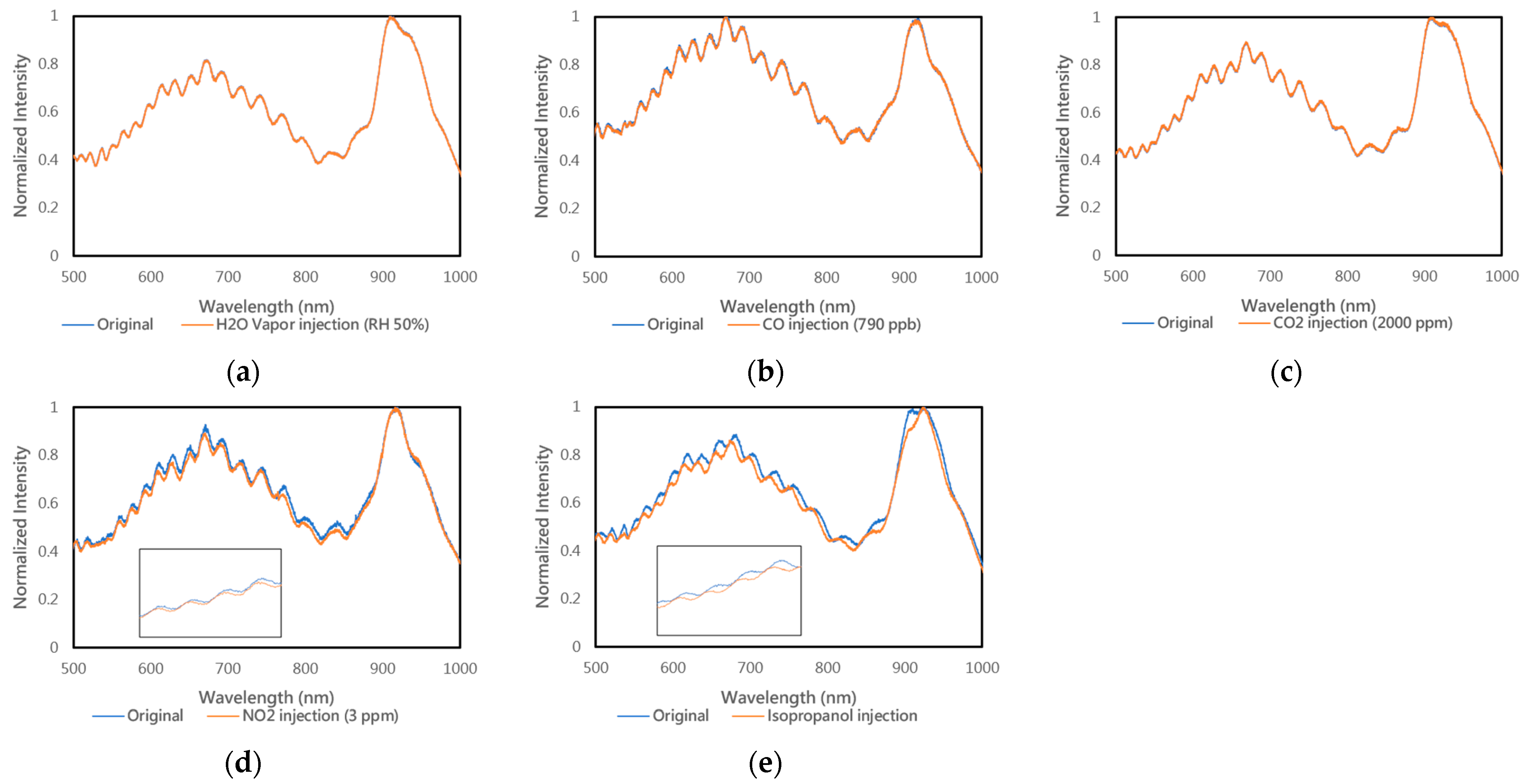
Figure 11 illustrates the changes in the interference spectrum of ZnO thin films before and after the injection of various gases. In this study, the Y-axis of the spectrum was normalized to reduce spectral deviations caused by different thin film sampling locations, facilitating more direct comparisons between the measurement results of various injected gases. According to the measurement outcomes, only nitrogen dioxide and gaseous isopropanol significantly impact the interference spectrum, with spectral peak shifts of 2.3 nm and 5.2 nm, respectively. This phenomenon may be attributed to several reasons: the gases, although adsorbed onto ZnO, may not induce changes in optical properties but rather in electrical resistance; alternatively, the intensity of the excitation light source might be insufficient, suggesting the use of higher-energy UV light or even lasers to facilitate reactions between ZnO and the gases.
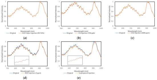
Figure 11.
Comparison of interference spectra before and after the injection of different gases: (a) after the injection of H2O vapor, the RH value increased from 30% to 50%, with no change observed in the interference spectrum; (b) following the injection of CO, no change occurred in the interference spectrum; (c) after injecting CO2, the interference spectrum remained unchanged; (d) upon the injection of NO2, a slight shift in the interference spectrum peaks towards lower wavelengths was observed, with an average shift of 2.3 nm; (e) after introducing isopropanol, a minor shift in the interference spectrum peaks towards lower wavelengths was noted, with an average shift of 5.2 nm.
Nonetheless, the current thin film interference spectroscopy setup demonstrates noticeable effectiveness in sensing NO2 and gaseous isopropanol, indicating a certain degree of selectivity in gas sensing with the current film and spectroscopic measurement approach. Future studies could further investigate these gases that show preliminary reactions.
4. Conclusions
In this study, a simple device for capturing the interference spectra of thin films was developed, incorporating a micro-spectrometer outfitted with a spectral chip and utilizing zinc oxide as the film under observation. Following the acquisition of ZnO’s interference spectra, numerical simulations were employed to deduce the film’s thickness and refractive index. The structure of the ZnO thin film, prepared via the sol–gel method, was determined through mathematical fitting to have a thickness of 4.9 μm and a refractive index (n) of 1.96 at 80 °C.
Subsequently, the film was placed in a gas chamber, with the micro-spectrometer continuously monitoring the interference spectrum to track changes on the film’s surface. Experimental results indicate that the optical properties of ZnO significantly vary with changes in environmental temperature, and a temperature calibration line can be established through the displacement of characteristic positions in the interference spectrum. In terms of gas sensing, the study tested several gases and found that NO2 and gaseous isopropanol could impact the interference spectrum of the ZnO film. Although the range of detectable gases is limited, this indicates that the method of measuring interference spectra possesses a degree of selectivity for gas detection. Future efforts could explore a broader array of gases or apply this approach to more types of thin films.
Supplementary Materials
The following supporting information can be downloaded at: https://www.mdpi.com/article/10.3390/micro4020019/s1, including results from SEM, EDS, simulations flow charts, and interference spectra.
Author Contributions
Conceptualization, C.-M.T. and Y.-C.H.; methodology, C.-M.T. and W.-Y.K.; software, C.-M.T.; validation, C.-M.T.; formal analysis, C.-M.T.; investigation, C.-M.T. and Y.-C.H.; resources, C.H. and C.-T.Y.; data curation, C.-M.T.; writing—original draft preparation, C.-M.T.; writing—review and editing, C.-M.T.; supervision, C.-H.K.; project administration, C.H. All authors have read and agreed to the published version of the manuscript.
Funding
This research was funded by NSTC (National Science and Technology Council), grant number is 111-2218-E-011-015-MBK.
Data Availability Statement
Measurement data and simulation flow charts are in the Supplementary Materials section.
Acknowledgments
The authors acknowledge the Industrial Technology Research Institute (ITRI) for providing material assistance and the Taiwan Instrument Research Institute (TIRI) for the use of testing instruments.
Conflicts of Interest
The authors declare no conflicts of interest.
References
- Laurenti, M.; Cauda, V. Porous Zinc Oxide Thin Films: Synthesis Approaches and Applications. Coatings 2018, 8, 67. [Google Scholar] [CrossRef]
- Txintxurreta, J.; G-Berasategui, E.; Ortiz, R.; Hernández, O.; Mendizábal, L.; Barriga, J. Indium Tin Oxide Thin Film Deposition by Magnetron Sputtering at Room Temperature for the Manufacturing of Efficient Transparent Heaters. Coatings 2021, 11, 92. [Google Scholar] [CrossRef]
- Thanka Rajan, S.; Subramanian, B.; Arockiarajan, A. A comprehensive review on biocompatible thin films for biomedical application. Ceram. Int. 2022, 48, 4377–4400. [Google Scholar] [CrossRef]
- Prieto-Cortés, P.; Álvarez-Tamayo, R.I.; García-Méndez, M.; Durán-Sánchez, M. Lossy Mode Resonance Generation on Sputtered Aluminum-Doped Zinc Oxide Thin Films Deposited on Multimode Optical Fiber Structures for Sensing Applications in the 1.55 µm Wavelength Range. Sensors 2019, 19, 4189. [Google Scholar] [CrossRef] [PubMed]
- Buonomenna, M.G. Inorganic Thin-Film Solar Cells: Challenges at the Terawatt-Scale. Symmetry 2023, 15, 1718. [Google Scholar] [CrossRef]
- Sabzi, M.; Mousavi Anijdan, S.H.; Shamsodin, M.; Farzam, M.; Hojjati-Najafabadi, A.; Feng, P.; Park, N.; Lee, U. A Review on Sustainable Manufacturing of Ceramic-Based Thin Films by Chemical Vapor Deposition (CVD): Reactions Kinetics and the Deposition Mechanisms. Coatings 2023, 13, 188. [Google Scholar] [CrossRef]
- Panjan, P.; Drnovšek, A.; Gselman, P.; Čekada, M.; Panjan, M. Review of Growth Defects in Thin Films Prepared by PVD Techniques. Coatings 2020, 10, 447. [Google Scholar] [CrossRef]
- Joshi, S.; Hegde, G.M.; Nayak, M.M.; Rajanna, K. A novel piezoelectric thin film impact sensor: Application in non-destructive material discrimination. Sens. Actuators A Phys. 2013, 199, 272–282. [Google Scholar] [CrossRef]
- Buchberger, A.; Peterka, S.; Coclite, A.M.; Bergmann, A. Fast Optical Humidity Sensor Based on Hydrogel Thin Film Expansion for Harsh Environment. Sensors 2019, 19, 999. [Google Scholar] [CrossRef]
- Ablekim, T.; Duenow, J.N.; Zheng, X.; Moutinho, H.; Moseley, J.; Perkins, C.L.; Johnston, S.W.; O’Keefe, P.; Colegrove, E.; Albin, D.S.; et al. Thin-Film Solar Cells with 19% Efficiency by Thermal Evaporation of CdSe and CdTe. ACS Energy Lett. 2020, 5, 892–896. [Google Scholar] [CrossRef]
- Colin, J.; Jamnig, A.; Furgeaud, C.; Michel, A.; Pliatsikas, N.; Sarakinos, K.; Abadias, G. In Situ and Real-Time Nanoscale Monitoring of Ultra-Thin Metal Film Growth Using Optical and Electrical Diagnostic Tools. Nanomaterials 2020, 10, 2225. [Google Scholar] [CrossRef] [PubMed]
- Navarro-Quezada, A.; Aiglinger, M.; Ghanbari, E.; Wagner, T.; Zeppenfeld, P. Polarization-dependent differential reflectance spectroscopy for real-time monitoring of organic thin film growth. Rev. Sci. Instrum. 2015, 86, 113108. [Google Scholar] [CrossRef] [PubMed]
- Losurdo, M.; Bergmair, M.; Bruno, G.; Cattelan, D.; Cobet, C.; de Martino, A.; Fleischer, K.; Dohcevic-Mitrovic, Z.; Esser, N.; Galliet, M.; et al. Spectroscopic ellipsometry and polarimetry for materials and systems analysis at the nanometer scale: State-of-the-art, potential, and perspectives. J. Nanoparticle Res. 2009, 11, 1521–1554. [Google Scholar] [CrossRef] [PubMed]
- Qiao, Q.; Liu, X.; Ren, Z.; Dong, B.; Xia, J.; Sun, H.; Lee, C.; Zhou, G. MEMS-Enabled On-Chip Computational Mid-Infrared Spectrometer Using Silicon Photonics. ACS Photonics 2022, 9, 2367–2377. [Google Scholar] [CrossRef]
- Eltagoury, Y.M.; Sabry, Y.M.; Khalil, D.A. All-Silicon Double-Cavity Fourier-Transform Infrared Spectrometer on-Chip. Adv. Mater. Technol. 2019, 4, 1900441. [Google Scholar] [CrossRef]
- Marvi, F.; Jafari, K.; Shahabadi, M.; Tabarzad, M.; Ghorbani-Bidkorpeh, F.; Azad, T. Ultrasensitive detection of vital biomolecules based on a multi-purpose BioMEMS for Point of care testing: Digoxin measurement as a case study. Sci. Rep. 2024, 14, 1633. [Google Scholar] [CrossRef]
- Chen, C.; Hu, H.; Li, X.; Zheng, Z.; Wang, Z.; Wang, X.; Zheng, P.; Cui, F.; Li, G.; Wang, Y.; et al. Rapid Detection of Anti-SARS-CoV-2 Antibody Using a Selenium Nanoparticle-Based Lateral Flow Immunoassay. IEEE Trans. NanoBioscience 2022, 21, 37–43. [Google Scholar] [CrossRef] [PubMed]
- Chiu, W.H.; Kong, W.Y.; Chueh, Y.H.; Wen, J.W.; Tsai, C.M.; Hong, C.; Chen, P.Y.; Ko, C.H. Using an ultra-compact optical system to improve lateral flow immunoassay results quantitatively. Heliyon 2022, 8, e12116. [Google Scholar] [CrossRef] [PubMed]
- Tamaekong, N.; Liewhiran, C.; Wisitsoraat, A.; Phanichphant, S. Flame-Spray-Made Undoped Zinc Oxide Films for Gas Sensing Applications. Sensors 2010, 10, 7863–7873. [Google Scholar] [CrossRef]
- Gartner, M.; Stroescu, H.; Mitrea, D.; Nicolescu, M. Various Applications of ZnO Thin Films Obtained by Chemical Routes in the Last Decade. Molecules 2023, 28, 4674. [Google Scholar] [CrossRef]
- Hu, S.-H.; Lin, Y.-S.; Su, S.-H.; He, J.-S.; Ai, Y.-Z. Improving Surface Structures of Al-Doped Zinc Oxide Thin Films to Apply in CO Gas-Sensing Property by Designing Processes through RF Magnetron Sputtering. J. Electron. Mater. 2024, 53, 2410–2420. [Google Scholar] [CrossRef]
- Kumar, V.; Singh, N.; Mehra, R.; Kapoor, A.; Purohit, L.; Swart, H. Role of film thickness on the properties of ZnO thin films grown by sol-gel method. Thin Solid Film. 2013, 539, 161–165. [Google Scholar] [CrossRef]
- Shariffudin, S.; Salina, M.; Herman, S.; Rusop, M. Effect of film thickness on structural, electrical, and optical properties of sol-gel deposited layer-by-layer ZnO nanoparticles. Trans. Electr. Electron. Mater. 2012, 13, 102–105. [Google Scholar] [CrossRef]
- Regmi, G.; Velumani, S. Impact of target power on the properties of sputtered intrinsic zinc oxide (i-ZnO) thin films and its thickness dependence performance on CISe solar cells. Opt. Mater. 2021, 119, 111350. [Google Scholar] [CrossRef]
- Sugianto, S.; Astuti, B.; Firmahaya, N.A.; Aryanto, D. The effect of annealing on ZnO:Al thin film growth on preparatory glass substrate by dc magnetron sputtering. J. Phys. Conf. Ser. 2019, 1387, 012007. [Google Scholar] [CrossRef]
- Ko, C.-H.; Tsai, S.-Y.; Tsai, J.-R.; Wang, B.-J. Design and verification of a flat-field aberration-corrected concave blaze grating for hyperspectral imaging. In Proceedings of the 2017 Conference on Lasers and Electro-Optics Pacific Rim (CLEO-PR), Singapore, 31 July–4 August 2017; pp. 1–4. [Google Scholar]
- Ko, C.-H.; Wu, Y.-H.; Chakraborty, S.; Shah, K.J.; Tsai, J.-R.; Wang, B.-J.; Lin, S.-F.; Hsiao, C.-D. Two-dimensional modeling with experimental verification of a linear variable filter for spectral order sorting of 400–1000 nm. In Proceedings of the 2017 Conference on Lasers and Electro-Optics Pacific Rim (CLEO-PR), Singapore, 31 July–4 August 2017; pp. 1–5. [Google Scholar]
- Sebők, D.; Szabó, T.; Dékány, I. Optical properties of zinc peroxide and zinc oxide multilayer nanohybrid films. Appl. Surf. Sci. 2009, 255, 6953–6962. [Google Scholar] [CrossRef]
- Janovák, L.; Dékány, I.; Sebők, D. The Theoretical Concept of Polarization Reflectometric Interference Spectroscopy (PRIFS): An Optical Method to Monitor Molecule Adsorption and Nanoparticle Adhesion on the Surface of Thin Films. Photonics 2019, 6, 76. [Google Scholar] [CrossRef]
- Amakali, T.; Daniel, L.S.; Uahengo, V.; Dzade, N.Y.; de Leeuw, N.H. Structural and Optical Properties of ZnO Thin Films Prepared by Molecular Precursor and Sol–Gel Methods. Crystals 2020, 10, 132. [Google Scholar] [CrossRef]
- Barth, J.; Johnson, R.L.; Cardona, M. Spectroscopic Ellipsometry in the 6–35 eV Region. In Handbook of Optical Constants of Solids; Palik, E.D., Ed.; Academic Press: Boston, MA, USA, 1998; Chapter 10; pp. 213–246. [Google Scholar]
- Gonçalves, R.S.; Barrozo, P.; Brito, G.L.; Viana, B.C.; Cunha, F. The effect of thickness on optical, structural and growth mechanism of ZnO thin film prepared by magnetron sputtering. Thin Solid Film. 2018, 661, 40–45. [Google Scholar] [CrossRef]
- Schinke, C.; Christian Peest, P.; Schmidt, J.; Brendel, R.; Bothe, K.; Vogt, M.R.; Kröger, I.; Winter, S.; Schirmacher, A.; Lim, S.; et al. Uncertainty analysis for the coefficient of band-to-band absorption of crystalline silicon. AIP Adv. 2015, 5. [Google Scholar] [CrossRef]
- Sulka, G.D. Electrochemistry of Thin Films and Nanostructured Materials. Molecules 2023, 28, 4040. [Google Scholar] [CrossRef] [PubMed]
- Teimoori, F.; Khojier, K.; Dehnavi, N.Z. On the Dependence of H2 Gas Sensitivity of ZnO thin Films on Film Thickness. Procedia Mater. Sci. 2015, 11, 474–479. [Google Scholar] [CrossRef][Green Version]
Disclaimer/Publisher’s Note: The statements, opinions and data contained in all publications are solely those of the individual author(s) and contributor(s) and not of MDPI and/or the editor(s). MDPI and/or the editor(s) disclaim responsibility for any injury to people or property resulting from any ideas, methods, instructions or products referred to in the content. |
© 2024 by the authors. Licensee MDPI, Basel, Switzerland. This article is an open access article distributed under the terms and conditions of the Creative Commons Attribution (CC BY) license (https://creativecommons.org/licenses/by/4.0/).


