
Pulsed Laser Deposition Method Used to Grow SiC Nanostructure on Porous Silicon Substrate: Synthesis and Optical Investigation for UV-Vis Photodetector Fabrication


Abstract
1. Introduction
2. Materials and Methods
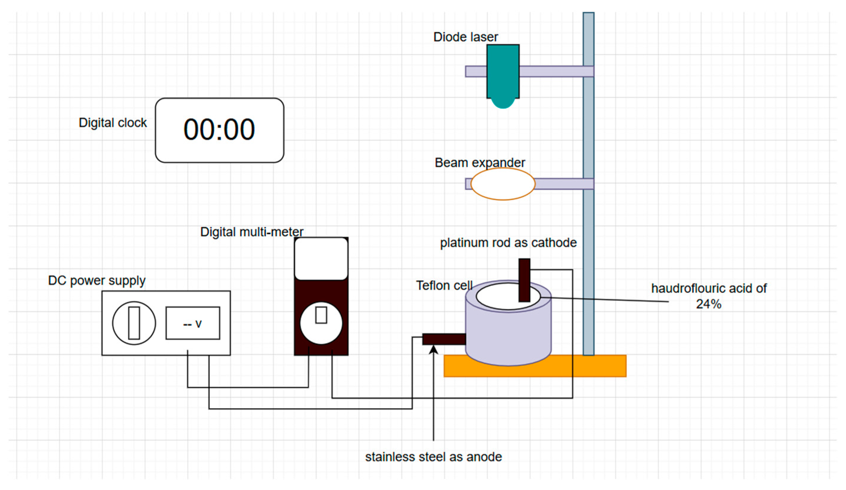
2.1. Fabrication of Porous Silicon (P-Si) Substrate
2.2. Fabrication of SiC Target
2.3. PLD for SiC Nanostructure Growth on P-Si Substrate
3. Results and Discussion
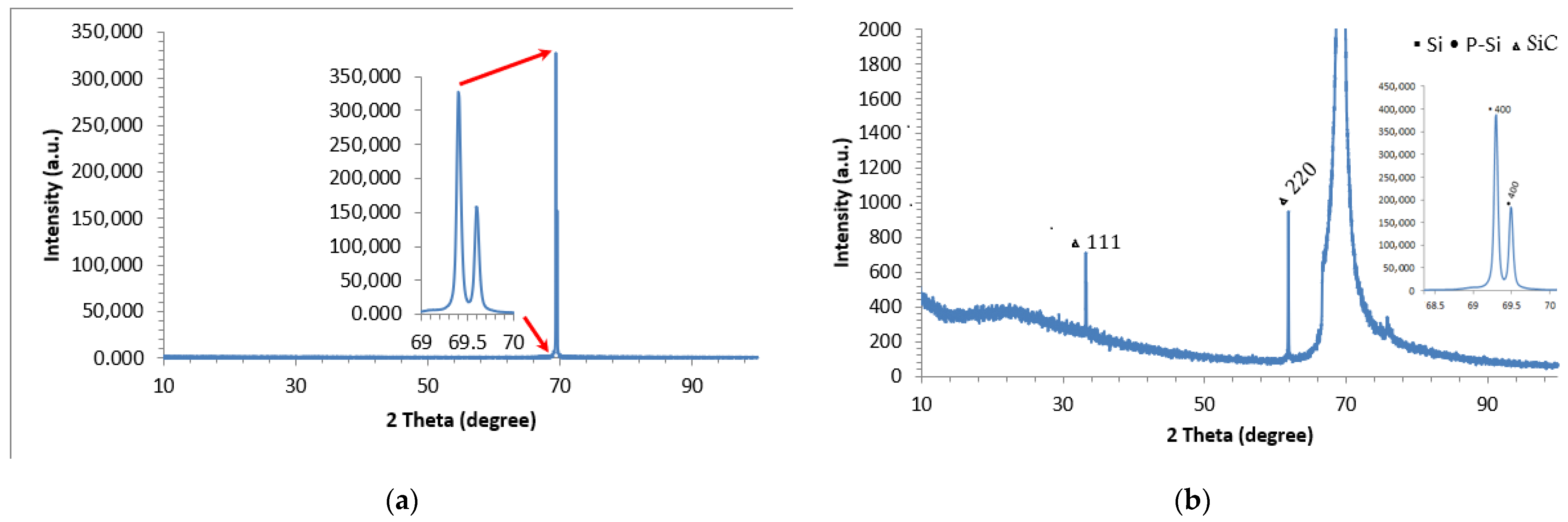
3.1. Structural Characteristic Analysis
3.2. Analysis of Spectroscopic Properties
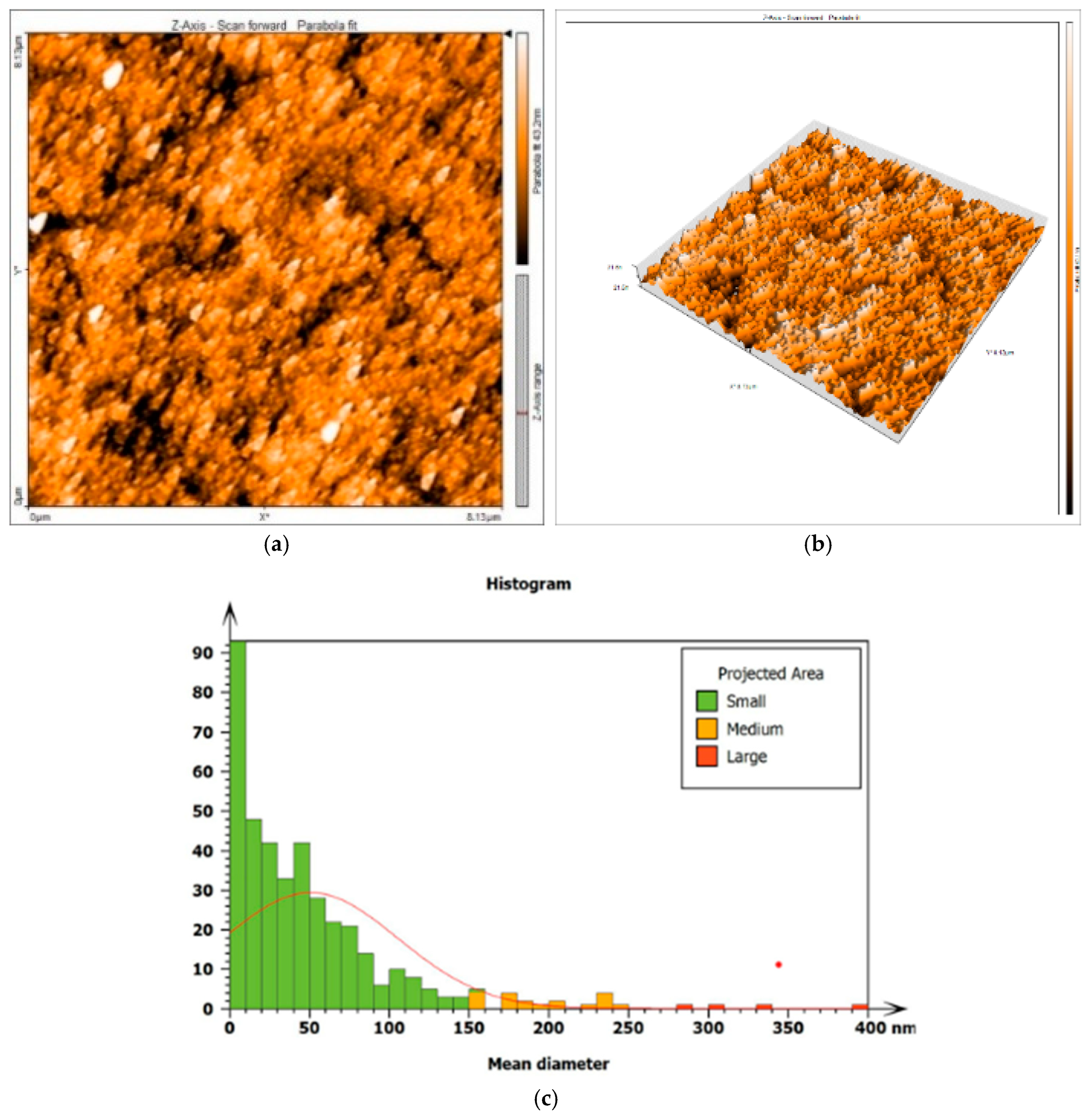
3.3. AFM Surface Topography
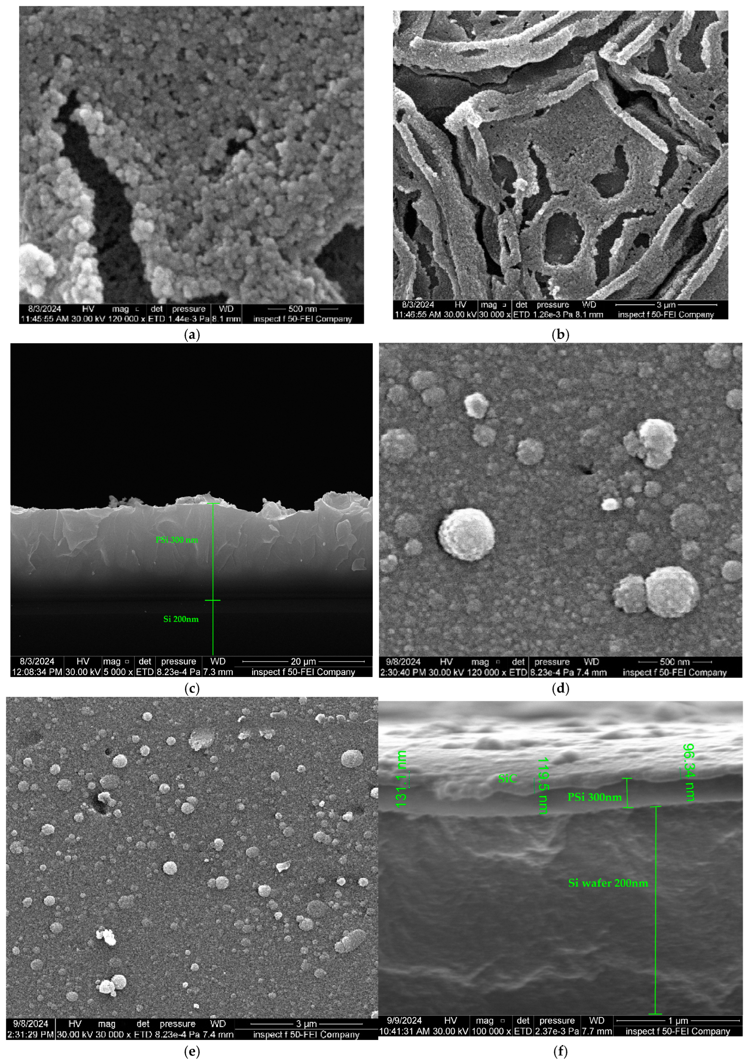
3.4. Surface Morphology FESEM
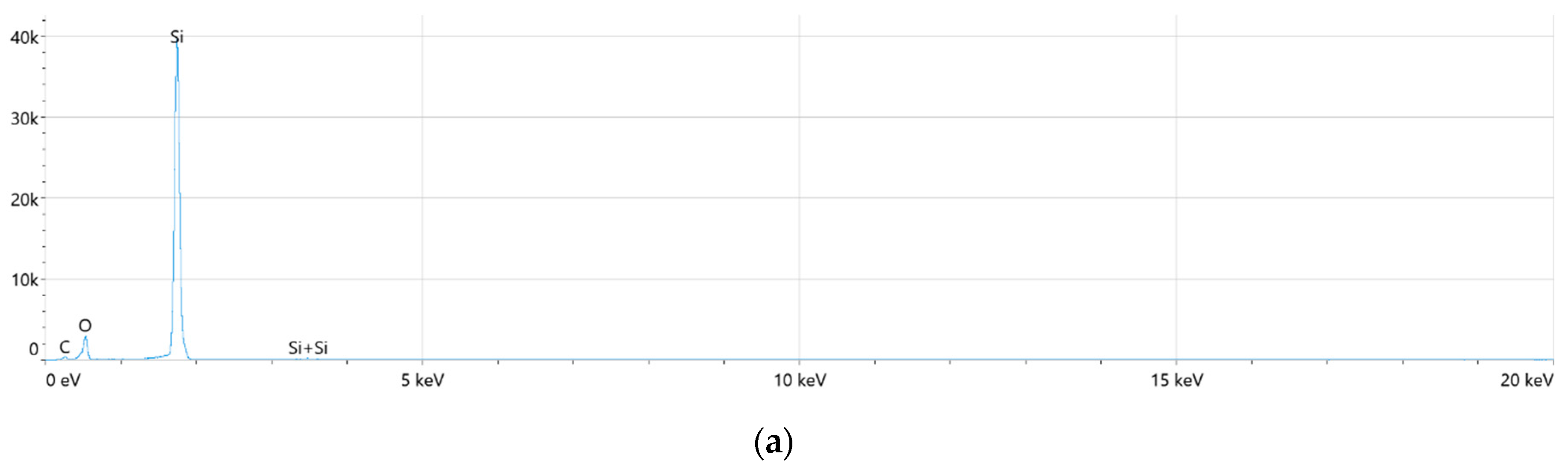
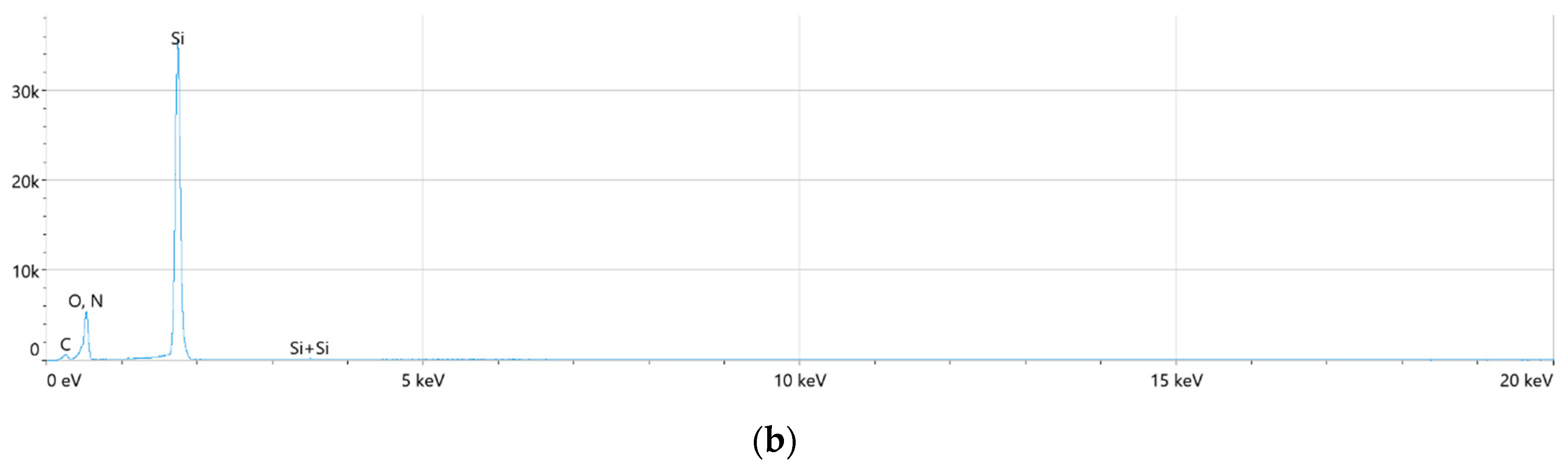
3.5. Energy-Dispersive X-Ray Spectroscopy (EDS)
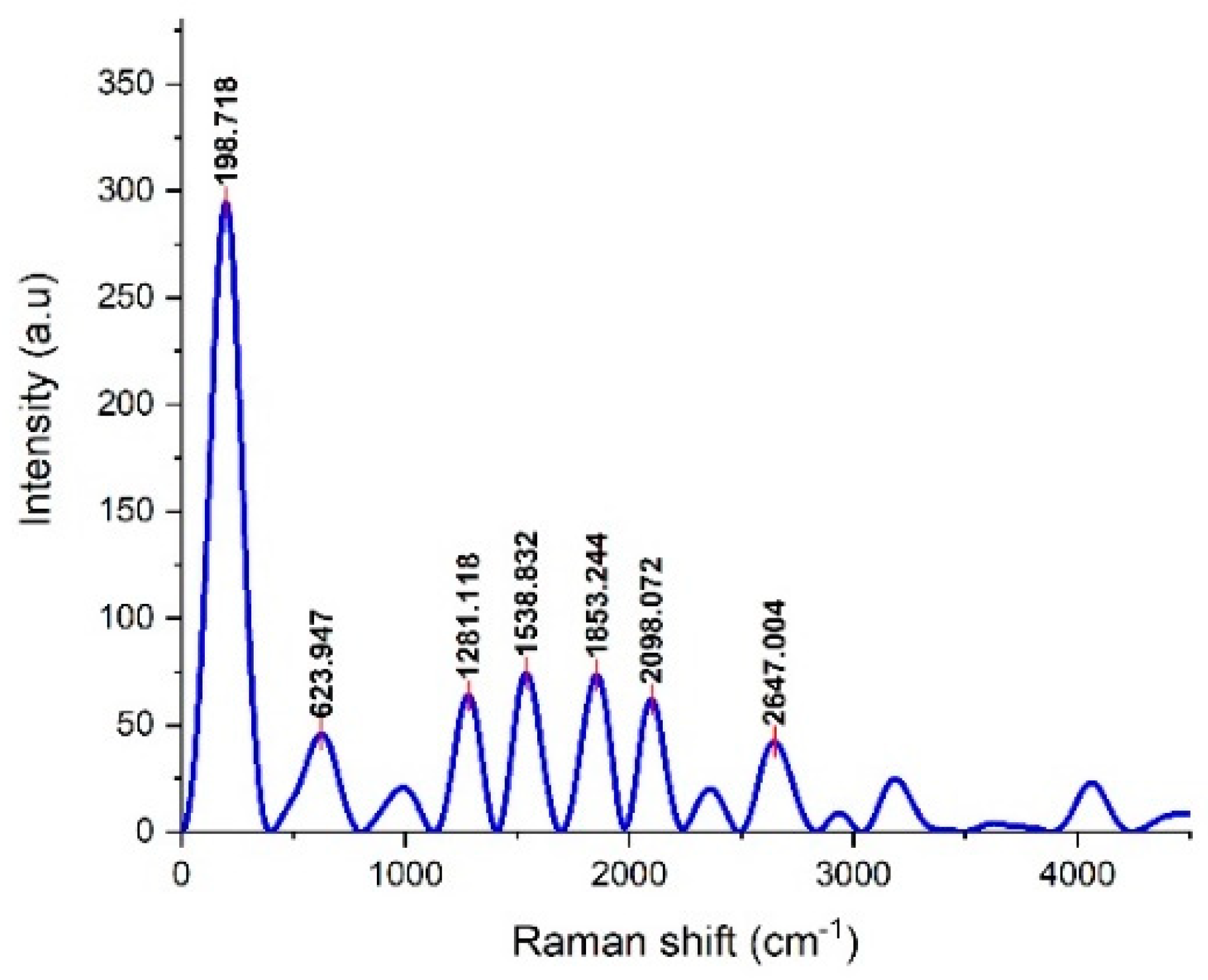
3.6. Raman Spectroscopy
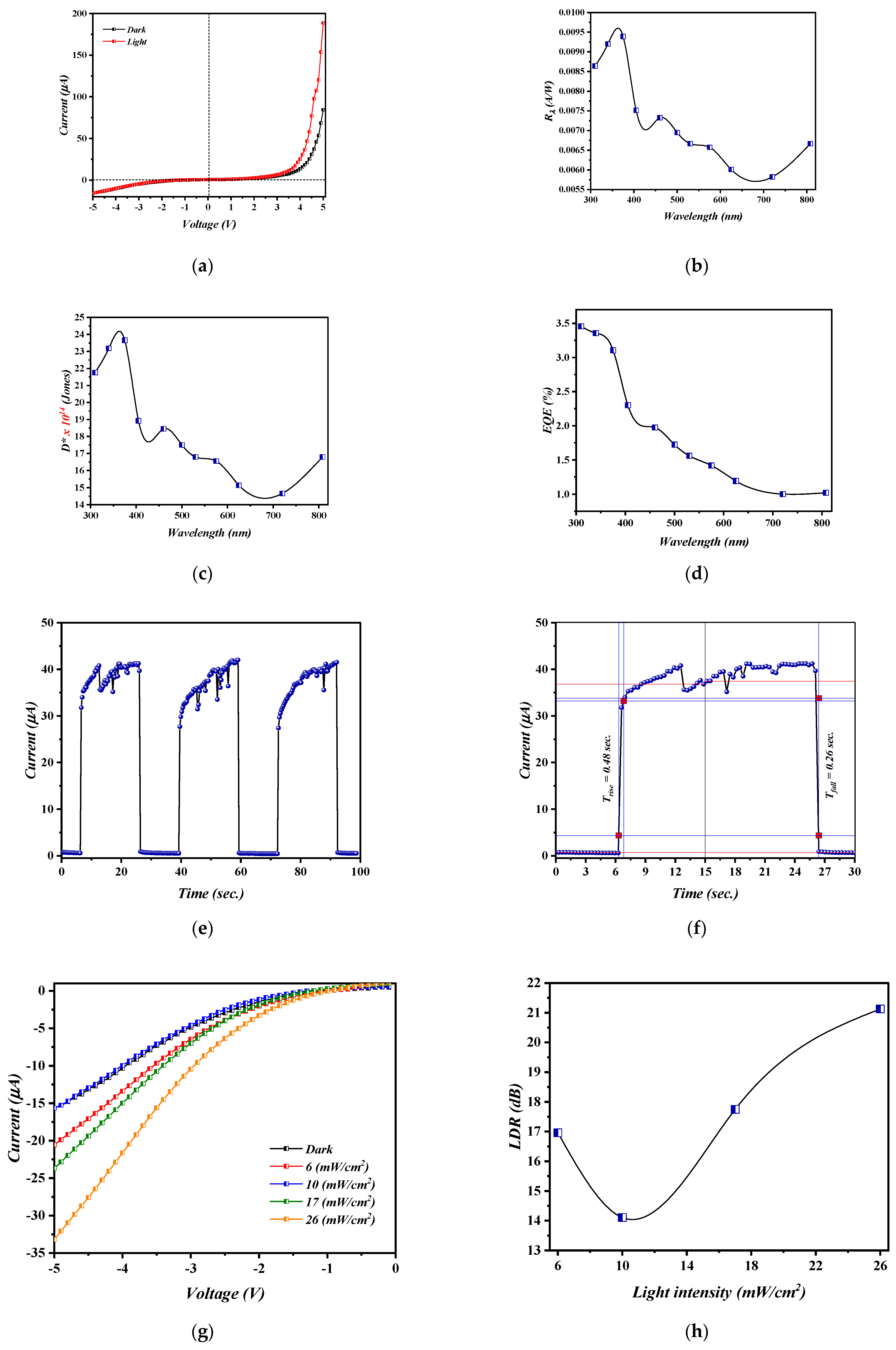
3.7. Electrical and Performance-Based Characteristics of SiC/P-Si
4. Conclusions
Author Contributions
Funding
Data Availability Statement
Acknowledgments
Conflicts of Interest
Abbreviations
| Nd: YAG | Neodymium-doped yttrium aluminum garnet |
| PLD | Pulsed laser deposition |
| AFM | Atomic force microscopy |
| FESEM | Field emission scanning electron microscopy |
| XRD | X-ray diffraction |
| P-Si | Porous silicon |
| SiC | Silicon carbide |
| LEDs | Light-emitting diodes |
| PL | Photoluminescence |
| EDS | Energy-dispersive X-ray spectroscopy |
References
- Morkoç, H.; Strite, S. GaN, AlN, and InN: A review of properties and processing. J. Appl. Phys. 1994, 76, 1363–1398. [Google Scholar] [CrossRef]
- Cao, F.; Liu, Y.; Liu, M.; Han, Z.; Xu, X.; Fan, Q.; Sun, B. Wide Bandgap Semiconductors for Ultraviolet Photodetectors. Research 2024, 2024, 0385. [Google Scholar] [CrossRef]
- Awawdeh, K.; Buttkewitz, M.A.; Bahnemann, J.; Segal, E. Enhancing the performance of porous silicon biosensors: The interplay of nanostructure design and microfluidic integration. Microsyst. Nanoeng. 2024, 10, 100. [Google Scholar] [CrossRef]
- Pearton, S.J.; Norton, D.P.; Ivill, M.; Hebard, A.F.; Zavada, J.M. Wide bandgap ferromagnetic for semiconductors and Oxide. J. Phys. Condens. Matter 2005, 16, R513–R537. [Google Scholar] [CrossRef]
- Miller, R.A.; So, H.; Heuser, T.A.; Senesky, D.G. High-temperature Ultraviolet Photodetectors: A Review. arXiv 2018, arXiv:1809.07396. [Google Scholar] [CrossRef]
- Salim, E.T.; Saimon, J.A.; Abood, M.K.; Fakhri, M.A. Effect of silicon substrate type on Nb2O5/Si device performance: An answer depends on physical analysis. Opt. Quantum Electron. 2020, 52, 463. [Google Scholar] [CrossRef]
- Salim, E.T.; Saimon, J.A.; Abood, M.K.; Fakhri, M.A. Electrical conductivity inversion for Nb2O5 nanostructure thin films at different temperatures. Mater. Res. Express 2019, 6, 126459. [Google Scholar] [CrossRef]
- Zhang, Q.; Liu, Y.; Li, H.; Wang, J.; Wang, Y.; Cheng, F.; Han, H.; Zhang, P. A Review of SiC Sensor Applications in High-Temperature and Radiation Extreme Environments. Sensors 2024, 24, 7731. [Google Scholar] [CrossRef]
- Naderi, N.; Hashim, M.R. Porous-shaped silicon carbide ultraviolet photodetectors on porous silicon substrates. J. Alloys Compd. 2013, 552, 356–362. [Google Scholar] [CrossRef]
- Hassan, M.A.M.; Al-Kadhemy, M.F.H.; Salem, E.T. Effect irradiation time of Gamma ray on MSISM (Au/SnO2/SiO2/Si/Al) devices using theoretical modeling. Int. J. Nanoelectron. Mater. 2015, 8, 69–82. [Google Scholar]
- Ismail, R.A.; Salim, E.T.; Halbos, H.T. Preparation of Nb2O5 nanoflakes by hydrothermal route for photodetection applications: The role of deposition time. Optik 2021, 245, 167778. [Google Scholar] [CrossRef]
- Zhang, X.; Wang, Y.; Liu, J. Raman spectroscopy of SiC thin films: Phonon modes and structural characterization. J. Appl. Phys. 2021, 130, 045302. [Google Scholar] [CrossRef]
- Chen, L.; Zhao, T.; Huang, M. Carbon defects in SiC and their influence on optical properties. Mater. Sci. Lett. 2020, 57, 178–186. [Google Scholar] [CrossRef]
- Lee, J.; Kwon, S.; Han, D. Phonon scattering in SiC/porous silicon heterostructures: A Raman study. Phys. Rev. Mater. 2019, 3, 075201. [Google Scholar] [CrossRef]
- Hassen, F.; M’Ghaieth, R.; Maaref, H.; Madar, R. Morphological and optical characterization of porous silicon carbide. Mater. Sci. Eng. B 2001, 85, 27–32. [Google Scholar] [CrossRef]
- Scuderi, V.; Muoio, A.; Sapienza, S.; La Via, F. Stress Fields Distribution and Simulation in 3C-SiC Resonators. Key Eng. Mater. 2024, 984, 41–46. [Google Scholar] [CrossRef]
- Abdul Muhsien, M.; Salem, E.T.; Agool, I.R. Preparation and characterization of (Au/n-SnO2/SiO2/Si/Al) MIS device for optoelectronic application. Int. J. Opt. 2013, 2013, 756402. [Google Scholar] [CrossRef]
- Xu, J.; Liu, S.; Yang, Y.; Li, J.; Tian, C.; Guo, L.; Zhang, S.; Liu, Y.; Zhong, Z. Preparation of porous silicon by electrochemical etching methods and its morphological and optical properties. Int. J. Electrochem. Sci. 2019, 14, 5095–5107. [Google Scholar] [CrossRef]
- International Centre for Diffraction Data (ICDD). Crystallographic Data for Silicon; PDF-2 Database, Card No. 27-1402; JCPDS: Newtown Square, PA, USA, 2003. [Google Scholar]
- Comedi, D.; Zalloum, O.H.Y.; Irving, E.A.; Wojcik, J.; Roschuk, T.; Flynn, M.J.; Mascher, P. X-ray-diffraction study of crystalline Si nanocluster formation in annealed silicon-rich silicon oxides. J. Appl. Phys. 2006, 99, 023518. [Google Scholar] [CrossRef]
- Zhou, X.; Zhang, X.; Li, L.; Sun, H. Surface and optical properties of silicon carbide grown by pulsed laser deposition. Thin Solid Film. 2011, 520, 3102–3107. [Google Scholar]
- Canham, L.T. Silicon quantum wire array fabrication by electrochemical and chemical dissolution of wafers. Appl. Phys. Lett. 1990, 57, 1046–1048. [Google Scholar] [CrossRef]
- Cullis, A.G.; Canham, L.T.; Calcott, P.D.J. The structural and luminescence properties of porous silicon. J. Appl. Phys. 1997, 82, 909–965. [Google Scholar] [CrossRef]
- Bright, R.; Brown, C.; Smith, T. Exploring the Challenges of Characterising Surface Topography of Nanomaterials. Nanomaterials 2024, 14, 1275. [Google Scholar] [CrossRef]
- Alfeel, F.; Awad, F.; Alghoraibi, I.; Qamar, F. Using AFM to determine the porosity in porous silicon. J. Mater. Sci. Eng. A 2012, 2, 579–583. Available online: https://www.researchgate.net/publication/279601246_Using_AFM_to_Determine_the_Porosity_in_Porous_Silicon (accessed on 26 March 2025).
- Salh, R. Defects in silicon and silicon carbide. In Crystalline Silicon—Properties and Uses; InTechOpen: London, UK, 2011. [Google Scholar] [CrossRef]
- Gelloz, B.; Kojima, T.; Koshida, N. Luminescence stability of porous silicon and its degradation mechanisms. Appl. Phys. Lett. 2002, 91, 2025–2028. [Google Scholar] [CrossRef]
- Neudeck, P.G.; Okojie, R.S.; Chen, L.Y. High-temperature electronics—A role for wide bandgap semiconductors? IEEE Trans. Electron Devices 1997, 44, 1123–1132. [Google Scholar] [CrossRef]
- Zhu, B.; Sun, C.; Chen, J.; Li, Z.; Huang, S.; Wu, S.; Lin, D.; Lin, Y.; Hong, R.; Chen, X.; et al. Tunable responsivity in high-performance SiC/graphene UV photodetectors through interfacial quantum states by bias regulation. Appl. Phys. Lett. 2023, 122, 163101. [Google Scholar] [CrossRef]
- Rogalski, A. Infrared Detectors: Status and Trends. Prog. Quantum Electron. 2003, 27, 59–210. [Google Scholar] [CrossRef]


| Element | Atomic % | Atomic % Error | Weight % | Weight % Error |
|---|---|---|---|---|
| C | 13.9 | 0.5 | 8.0 | 0.3 |
| O | 41.6 | 0.4 | 31.9 | 0.3 |
| Si | 44.5 | 0.2 | 60.1 | 0.2 |
| Element | Atomic % | Atomic % Error | Weight % | Weight % Error |
|---|---|---|---|---|
| C | 15.1 | 0.5 | 9.7 | 0.3 |
| N | 7.4 | 0.5 | 5.5 | 0.4 |
| O | 48.8 | 0.4 | 41.7 | 0.3 |
| Si | 28.8 | 0.1 | 43.1 | 0.2 |
Disclaimer/Publisher’s Note: The statements, opinions and data contained in all publications are solely those of the individual author(s) and contributor(s) and not of MDPI and/or the editor(s). MDPI and/or the editor(s) disclaim responsibility for any injury to people or property resulting from any ideas, methods, instructions or products referred to in the content. |
© 2025 by the authors. Licensee MDPI, Basel, Switzerland. This article is an open access article distributed under the terms and conditions of the Creative Commons Attribution (CC BY) license (https://creativecommons.org/licenses/by/4.0/).
Share and Cite
Alzubaidi, R.; Fakhri, M.A.; Pohl, L. Pulsed Laser Deposition Method Used to Grow SiC Nanostructure on Porous Silicon Substrate: Synthesis and Optical Investigation for UV-Vis Photodetector Fabrication. Thermo 2025, 5, 13. https://doi.org/10.3390/thermo5020013
Alzubaidi R, Fakhri MA, Pohl L. Pulsed Laser Deposition Method Used to Grow SiC Nanostructure on Porous Silicon Substrate: Synthesis and Optical Investigation for UV-Vis Photodetector Fabrication. Thermo. 2025; 5(2):13. https://doi.org/10.3390/thermo5020013
Chicago/Turabian StyleAlzubaidi, Reem, Makram A. Fakhri, and László Pohl. 2025. "Pulsed Laser Deposition Method Used to Grow SiC Nanostructure on Porous Silicon Substrate: Synthesis and Optical Investigation for UV-Vis Photodetector Fabrication" Thermo 5, no. 2: 13. https://doi.org/10.3390/thermo5020013
APA StyleAlzubaidi, R., Fakhri, M. A., & Pohl, L. (2025). Pulsed Laser Deposition Method Used to Grow SiC Nanostructure on Porous Silicon Substrate: Synthesis and Optical Investigation for UV-Vis Photodetector Fabrication. Thermo, 5(2), 13. https://doi.org/10.3390/thermo5020013