
A Review of Recent Developments in Smart Textiles Based on Perovskite Materials


Abstract
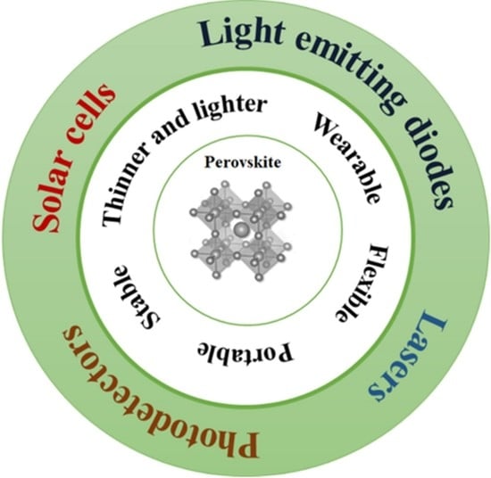
1. Introduction
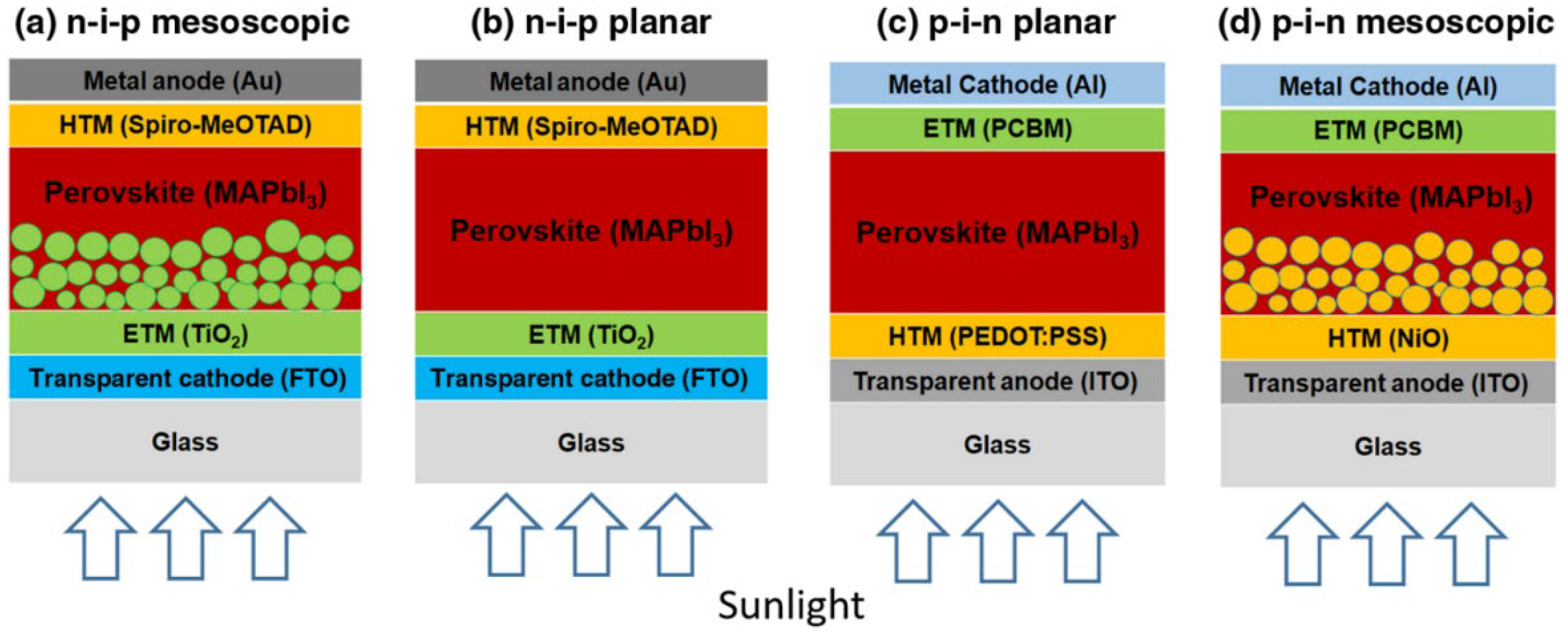
2. Perovskite Device Structures and Working Mechanisms
2.1. Solar Cells
2.2. Light-Emitting Diodes (LEDs)
2.3. Photodetectors
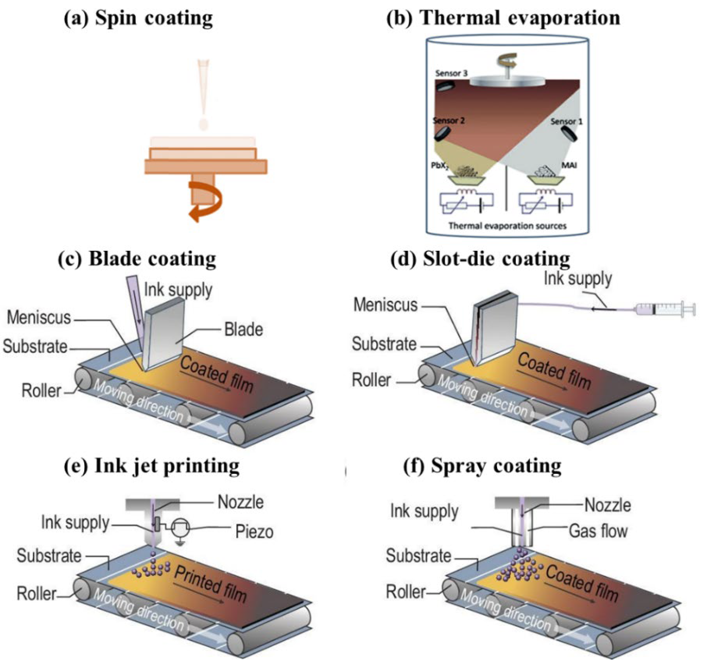
3. Manufacturing Techniques
3.1. Spin Coating
3.2. Thermal Evaporation
3.3. Roll-to-Roll Manufacturing
3.3.1. Inkjet Printing
3.3.2. Slot-Die Coating
3.3.3. Spray Coating
3.3.4. Blade Coating
4. Textile-Based Perovskite Optoelectronic Applications
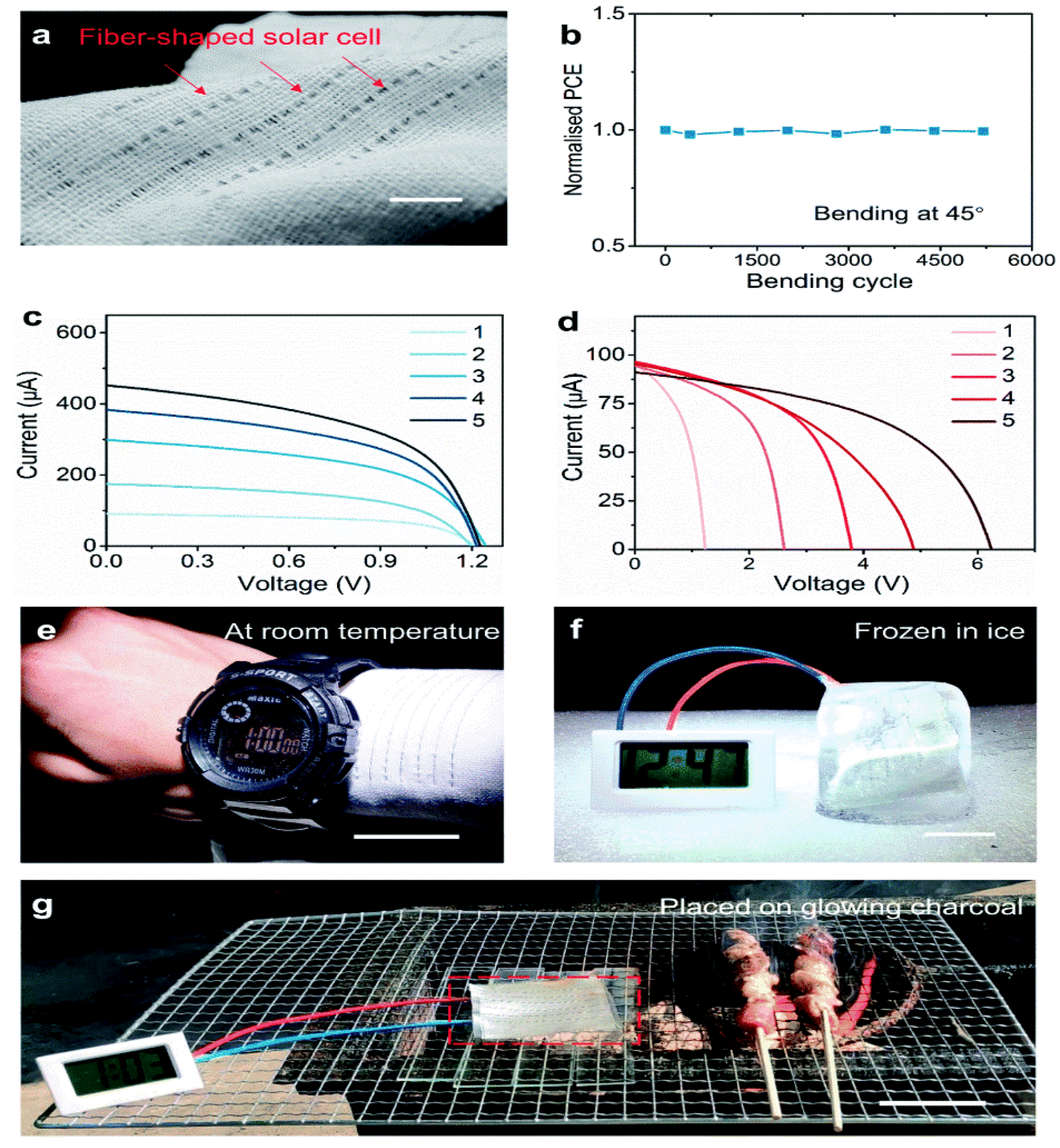
4.1. Wearable Solar Cells
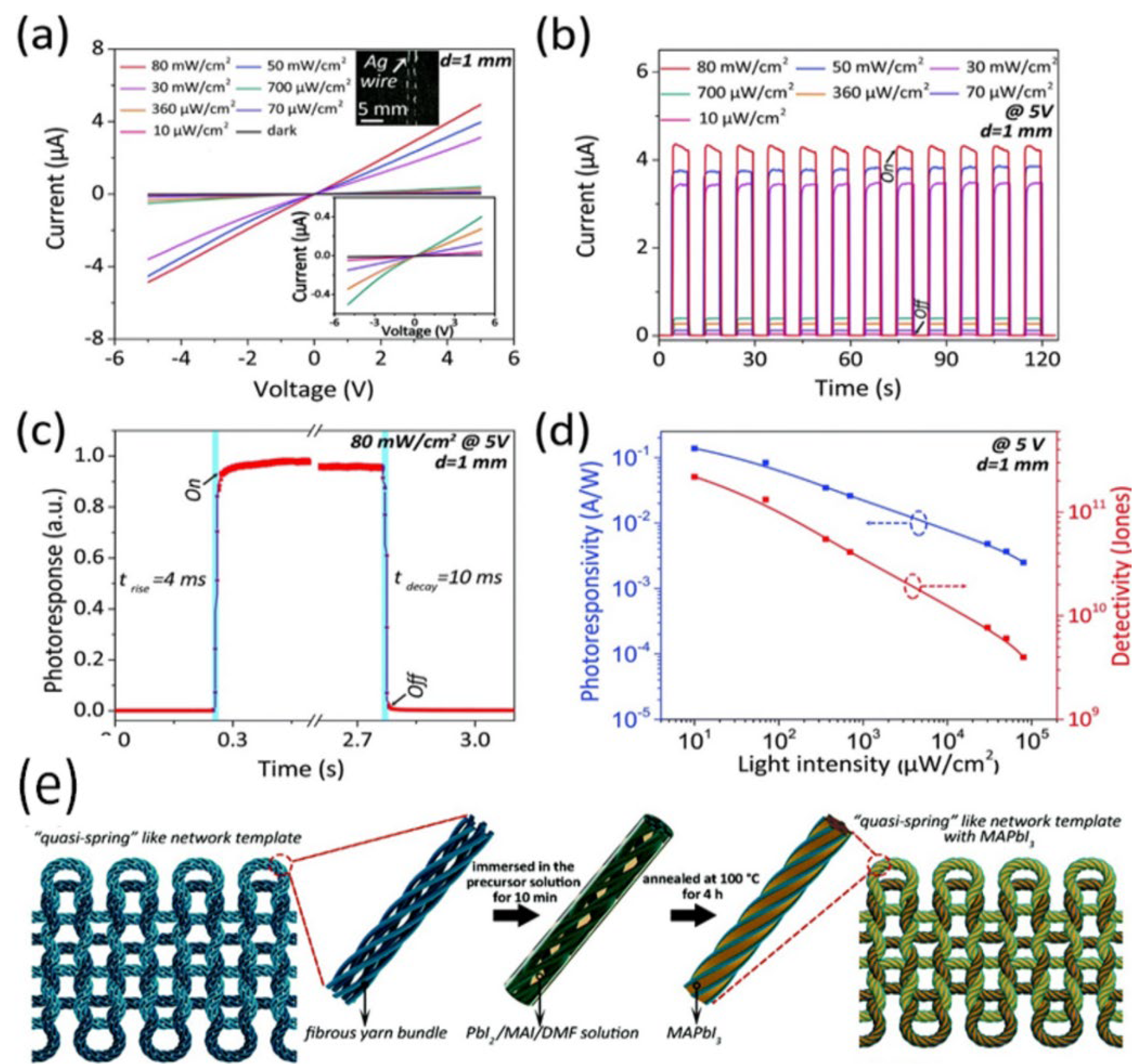
4.2. Photodetectors for Wearable Optoelectronics
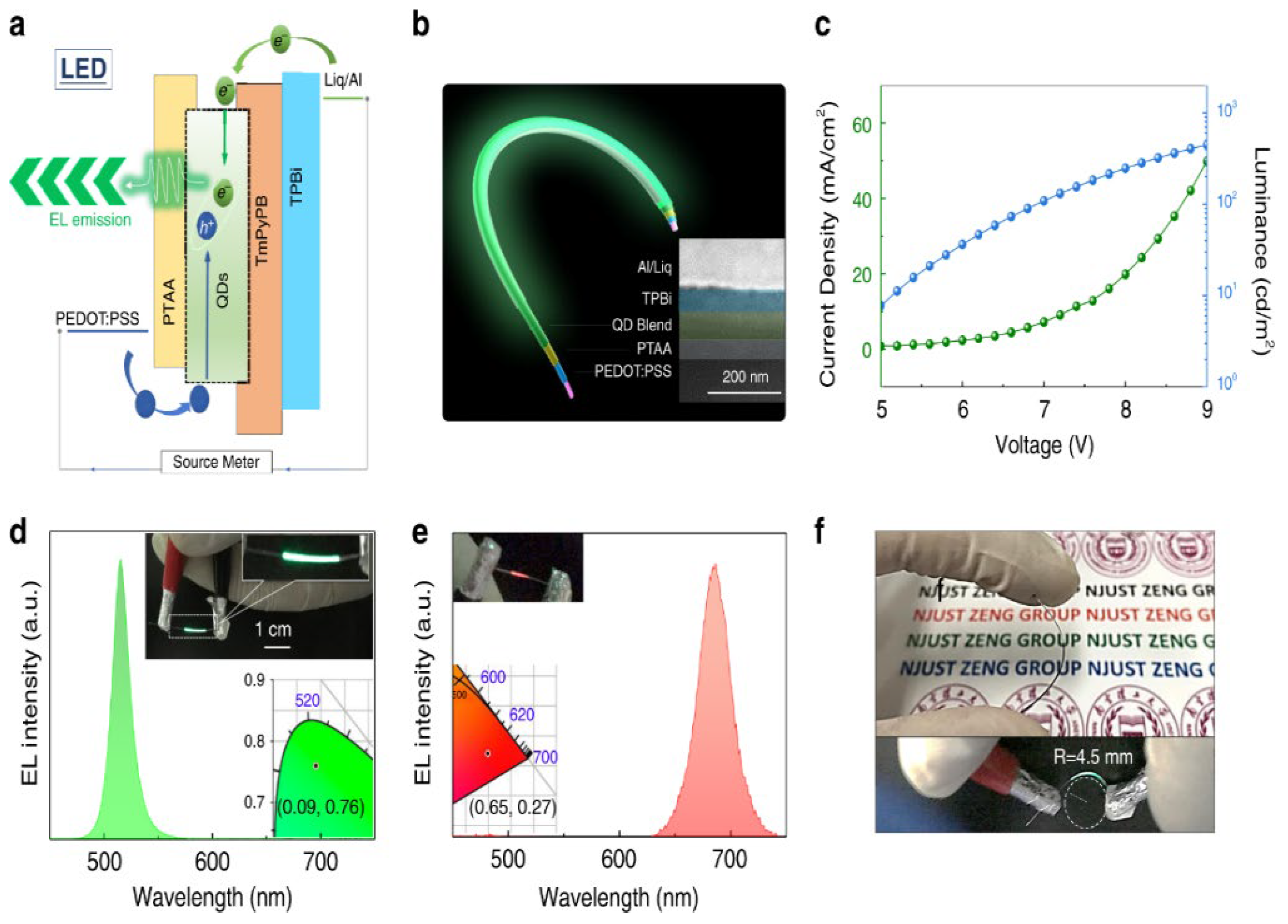
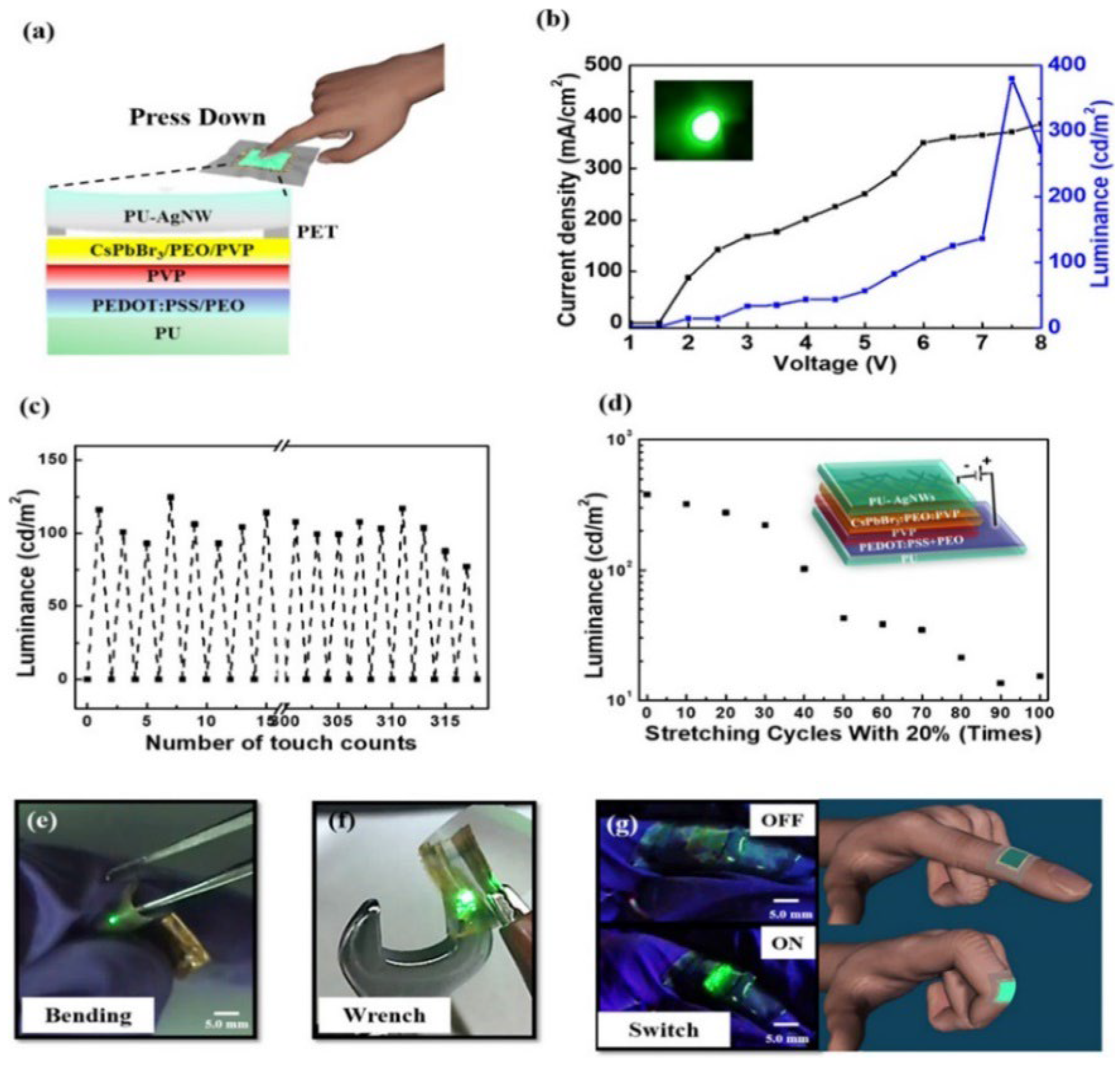
4.3. Fibre- and Fabric-Based Perovskite Light-Emitting Diodes
5. Challenges and Future Perspectives
Author Contributions
Funding
Institutional Review Board Statement
Informed Consent Statement
Acknowledgments
Conflicts of Interest
References
- Xu, L.; Fu, X.; Liu, F.; Shi, X.; Zhou, X.; Liao, M.; Chen, C.; Xu, F.; Wang, B.; Zhang, B.; et al. A perovskite solar cell textile that works at −40 to 160 °C. J. Mater. Chem. A 2020, 8, 5476–5483. [Google Scholar] [CrossRef]
- Wang, Y.; Li, D.; Chao, L.; Niu, T.; Chen, Y.; Huang, W. Perovskite photodetectors for flexible electronics: Recent advances and perspectives. Appl. Mater. Today 2022, 28, 101509. [Google Scholar] [CrossRef]
- Zhang, Q.; Yin, Y. All-Inorganic Metal Halide Perovskite Nanocrystals: Opportunities and Challenges. ACS Central Sci. 2018, 4, 668–679. [Google Scholar] [CrossRef] [PubMed]
- Liu, M.; Ali-Löytty, H.; Hiltunen, A.; Sarlin, E.; Qudsia, S.; Smått, J.; Valden, M.; Vivo, P. Manganese Doping Promotes the Synthesis of Bismuth-based Perovskite Nanocrystals While Tuning Their Band Structures. Small 2021, 17, 2100101. [Google Scholar] [CrossRef]
- Liu, M.; Pasanen, H.; Ali-Löytty, H.; Hiltunen, A.; Lahtonen, K.; Qudsia, S.; Smått, J.; Valden, M.; Tkachenko, N.V.; Vivo, P. B-Site Co-Alloying with Germanium Improves the Efficiency and Stability of All-Inorganic Tin-Based Perovskite Nanocrystal Solar Cells. Angew. Chem. 2020, 132, 22301–22309. [Google Scholar] [CrossRef]
- Tabassum, M.; Zia, Q.; Zhou, Y.; Reece, M.J.; Su, L. A review on advances in doping with alkali metals in halide perovskite materials. SN Appl. Sci. 2021, 3, 888. [Google Scholar] [CrossRef]
- Ha, S.-T.; Su, R.; Xing, J.; Zhang, Q.; Xiong, Q. Metal halide perovskite nanomaterials: Synthesis and applications. Chem. Sci. 2017, 8, 2522–2536. [Google Scholar] [CrossRef]
- Kojima, A.; Teshima, K.; Shirai, Y.; Miyasaka, T. Organometal Halide Perovskites as Visible-Light Sensitizers for Photovoltaic Cells. J. Am. Chem. Soc. 2009, 131, 6050–6051. [Google Scholar] [CrossRef]
- Kumar, M.H.; Yantara, N.; Dharani, S.; Graetzel, M.; Mhaisalkar, S.; Boix, P.P.; Mathews, N. Flexible, low-temperature, solution processed ZnO-based perovskite solid state solar cells. Chem. Commun. 2013, 49, 11089–11091. [Google Scholar] [CrossRef]
- Yang, L.; Xiong, Q.; Li, Y.; Gao, P.; Xu, B.; Lin, H.; Li, X.; Miyasaka, T. Artemisinin-passivated mixed-cation perovskite films for durable flexible perovskite solar cells with over 21% efficiency. J. Mater. Chem. A 2021, 9, 1574–1582. [Google Scholar] [CrossRef]
- Jia, P.; Lu, M.; Sun, S.; Gao, Y.; Wang, R.; Zhao, X.; Sun, G.; Colvin, V.L.; Yu, W.W. Recent Advances in Flexible Perovskite Light-Emitting Diodes. Adv. Mater. Interfaces 2021, 8, 2100441. [Google Scholar] [CrossRef]
- Shen, Y.; Li, M.-N.; Li, Y.; Xie, F.-M.; Wu, H.-Y.; Zhang, G.-H.; Chen, L.; Lee, S.-T.; Tang, J.-X. Rational Interface Engineering for Efficient Flexible Perovskite Light-Emitting Diodes. ACS Nano 2020, 14, 6107–6116. [Google Scholar] [CrossRef]
- Hu, X.; Zhang, X.; Liang, L.; Bao, J.; Li, S.; Yang, W.; Xie, Y. High-Performance Flexible Broadband Photodetector Based on Organolead Halide Perovskite. Adv. Funct. Mater. 2014, 24, 7373–7380. [Google Scholar] [CrossRef]
- Chen, H.; Wang, H.; Wu, J.; Wang, F.; Zhang, T.; Wang, Y.; Liu, D.; Li, S.; Penty, R.V.; White, I.H. Flexible optoelectronic devices based on metal halide perovskites. Nano Res. 2020, 13, 1997–2018. [Google Scholar] [CrossRef]
- Zhao, R.; Gu, Z.; Li, P.; Zhang, Y.; Song, Y. Flexible and Wearable Optoelectronic Devices Based on Perovskites. Adv. Mater. Technol. 2022, 7, 2101124. [Google Scholar] [CrossRef]
- Li, K.; Xiao, J.; Yu, X.; Li, T.; Xiao, D.; He, J.; Zhou, P.; Zhang, Y.; Li, W.; Ku, Z.; et al. An efficient, flexible perovskite solar module exceeding 8% prepared with an ultrafast PbI2 deposition rate. Sci. Rep. 2018, 8, 442. [Google Scholar] [CrossRef]
- Gao, B.-W.; Meng, J. Large area and flexible CH3NH3PbI3 perovskite solar cell fabricated by all ink jet printing. Acta Phys. Sin. 2021, 70, 208801. [Google Scholar] [CrossRef]
- Gao, B.; Meng, J. Flexible CH3NH3PbI3 perovskite solar cells with high stability based on all inkjet printing. Sol. Energy 2021, 230, 598–604. [Google Scholar] [CrossRef]
- Kim, Y.Y.; Yang, T.-Y.; Suhonen, R.; Kemppainen, A.; Hwang, K.; Jeon, N.J.; Seo, J. Roll-to-roll gravure-printed flexible perovskite solar cells using eco-friendly antisolvent bathing with wide processing window. Nat. Commun. 2020, 11, 5146. [Google Scholar] [CrossRef]
- Ou, X.-L.; Xu, M.; Feng, J.; Sun, H.-B. Flexible and efficient ITO-free semitransparent perovskite solar cells. Sol. Energy Mater. Sol. Cells 2016, 157, 660–665. [Google Scholar] [CrossRef]
- Qin, F.; Tong, J.; Ge, R.; Luo, B.; Jiang, F.; Liu, T.; Jiang, Y.; Xu, Z.; Mao, L.; Meng, W.; et al. Indium tin oxide (ITO)-free, top-illuminated, flexible perovskite solar cells. J. Mater. Chem. A 2016, 4, 14017–14024. [Google Scholar] [CrossRef]
- Li, Y.; Meng, L.; Yang, Y.M.; Xu, G.; Hong, Z.; Chen, Q.; You, J.; Li, G.; Li, Y. High-efficiency robust perovskite solar cells on ultrathin flexible substrates. Nat. Commun. 2016, 7, 10214. [Google Scholar] [CrossRef] [PubMed]
- Hou, L.; Wang, Y.; Liu, X.; Wang, J.; Wang, L.; Li, X.; Fu, G.; Yang, S. 18.0% efficiency flexible perovskite solar cells based on double hole transport layers and CH3NH3PbI3−xClx with dual additives. J. Mater. Chem. C 2018, 6, 8770–8777. [Google Scholar] [CrossRef]
- De Rossi, F.; Taheri, B.; Bonomo, M.; Gupta, V.; Renno, G.; Nia, N.Y.; Rech, P.; Frost, C.; Cazzaniga, C.; Quagliotto, P.; et al. Neutron irradiated perovskite films and solar cells on PET substrates. Nano Energy 2022, 93, 106879. [Google Scholar] [CrossRef]
- Clark, M. (Ed.) Handbook of Textile and Industrial Dyeing; Elsevier: Amsterdam, The Netherlands, 2011; Volume 2. [Google Scholar]
- Xu, Y.; Lin, Z.; Wei, W.; Hao, Y.; Liu, S.; Ouyang, J.; Chang, J. Recent Progress of Electrode Materials for Flexible Perovskite Solar Cells. Nano-Micro Lett. 2022, 14, 117. [Google Scholar] [CrossRef] [PubMed]
- Tang, G.; Yan, F. Recent progress of flexible perovskite solar cells. Nano Today 2021, 39, 101155. [Google Scholar] [CrossRef]
- Yang, D.; Yang, R.; Priya, S.; Liu, F. Recent Advances in Flexible Perovskite Solar Cells: Fabrication and Applications. Angew. Chem. Int. Ed. 2019, 58, 4466–4483. [Google Scholar] [CrossRef]
- Liang, X.; Ge, C.; Fang, Q.; Deng, W.; Dey, S.; Lin, H.; Zhang, Y.; Zhang, X.; Zhu, Q.; Hu, H. Flexible Perovskite Solar Cells: Progress and Prospects. Front. Mater. 2021, 8, 634353. [Google Scholar] [CrossRef]
- Qiu, L.; Deng, J.; Lü, X.; Yang, Z.; Peng, H. Inside Cover: Integrating Perovskite Solar Cells into a Flexible Fiber (Angew. Chem. Int. Ed. 39/2014). Angew. Chem. Int. Ed. 2014, 53, 10254. [Google Scholar] [CrossRef][Green Version]
- Qiu, L.; Deng, J.; Lü, X.; Yang, Z.; Peng, H. Innentitelbild: Integrating Perovskite Solar Cells into a Flexible Fiber (Angew. Chem. 39/2014). Angew. Chem. 2014, 126, 10420. [Google Scholar] [CrossRef]
- Xu, X.; Sun, L.; Shen, K.; Zhang, S. Organic and hybrid organic-inorganic flexible optoelectronics: Recent advances and perspectives. Synth. Met. 2019, 256, 116137. [Google Scholar] [CrossRef]
- Hussain, I.; Tran, H.P.; Jaksik, J.; Moore, J.; Islam, N.; Uddin, M.J. Functional materials, device architecture, and flexibility of perovskite solar cell. Emergent Mater. 2018, 1, 133–154. [Google Scholar] [CrossRef]
- Chen, Z.; Li, Z.; Hopper, T.R.; Bakulin, A.A.; Yip, H.-L. Materials, photophysics and device engineering of perovskite light-emitting diodes. Rep. Prog. Phys. 2021, 84, 046401. [Google Scholar] [CrossRef]
- Zhao, C.; Zhang, D.; Qin, C. Perovskite Light-Emitting Diodes. CCS Chem. 2020, 2, 859–869. [Google Scholar] [CrossRef]
- Ji, K.; Anaya, M.; Abfalterer, A.; Stranks, S.D. Halide Perovskite Light-Emitting Diode Technologies. Adv. Opt. Mater. 2021, 9, 2002128. [Google Scholar] [CrossRef]
- Trudeau, C.; Bolduc, M.; Beaupre, P.; Ka, I.; Asuo, I.M.; Cloutier, S.G. Inkjet-Printing of Methylammonium Lead Trihalide Perovskite-Based Flexible Optoelectronic Devices. In Proceedings of the 2018 International Flexible Electronics Technology Conference (IFETC), Ottawa, ON, Canada, 7–9 August 2018; pp. 1–6. [Google Scholar] [CrossRef]
- Li, G.; Wang, Y.; Huang, L.; Sun, W. Research Progress of High-Sensitivity Perovskite Photodetectors: A Review of Photodetectors: Noise, Structure, and Materials. ACS Appl. Electron. Mater. 2022, 4, 1485–1505. [Google Scholar] [CrossRef]
- Yoo, J.J.; Shin, S.S.; Seo, J. Toward Efficient Perovskite Solar Cells: Progress, Strategies, and Perspectives. ACS Energy Lett. 2022, 7, 2084–2091. [Google Scholar] [CrossRef]
- Angmo, D.; DeLuca, G.; Scully, A.D.; Chesman, A.S.; Seeber, A.; Zuo, C.; Vak, D.; Bach, U.; Gao, M. A Lab-to-Fab Study toward Roll-to-Roll Fabrication of Reproducible Perovskite Solar Cells under Ambient Room Conditions. Cell Rep. Phys. Sci. 2021, 2, 100293. [Google Scholar] [CrossRef]
- Yang, T.-Y.; Kim, Y.Y.; Seo, J. Roll-to-roll manufacturing toward lab-to-fab-translation of perovskite solar cells. APL Mater. 2021, 9, 110901. [Google Scholar] [CrossRef]
- Pratap, S.; Babbe, F.; Barchi, N.S.; Yuan, Z.; Luong, T.; Haber, Z.; Song, T.-B.; Slack, J.L.; Stan, C.V.; Tamura, N.; et al. Out-of-equilibrium processes in crystallization of organic-inorganic perovskites during spin coating. Nat. Commun. 2021, 12, 5624. [Google Scholar] [CrossRef]
- Baker, J.A.; Mouhamad, Y.; Hooper, K.E.; Burkitt, D.; Geoghegan, M.; Watson, T.M. From spin coating to roll-to-roll: Investigating the challenge of upscaling lead halide perovskite solar cells. IET Renew. Power Gener. 2017, 11, 546–549. [Google Scholar] [CrossRef]
- Konstantakou, M.; Perganti, D.; Falaras, P.; Stergiopoulos, T. Anti-Solvent Crystallization Strategies for Highly Efficient Perovskite Solar Cells. Crystals 2017, 7, 291. [Google Scholar] [CrossRef]
- Pola, S.; Panwar, N.; Coondoo, I. (Eds.) Perovskite and Piezoelectric Materials; IntechOpen: Vienna, Austria, 2021. [Google Scholar]
- Zhang, J.; Zhang, W.; Cheng, H.-M.; Silva, S.R.P. Critical review of recent progress of flexible perovskite solar cells. Mater. Today 2020, 39, 66–88. [Google Scholar] [CrossRef]
- Gupta, R.K.; Nguyen, T.A. (Eds.) Smart and Flexible Energy Devices; CRC Press: Boca Raton, FL, USA, 2022. [Google Scholar]
- Era, M.; Hattori, T.; Taira, T.; Tsutsui, T. Self-Organized Growth of PbI-Based Layered Perovskite Quantum Well by Dual-Source Vapor Deposition. Chem. Mater. 1997, 9, 8–10. [Google Scholar] [CrossRef]
- Tavakoli, M.M.; Tavakoli, R. All-Vacuum-Processing for Fabrication of Efficient, Large-Scale, and Flexible Inverted Perovskite Solar Cells. Phys. Status Solidi (RRL) Rapid Res. Lett. 2021, 15, 2000449. [Google Scholar] [CrossRef]
- Li, J.; Yang, L.; Guo, Q.; Du, P.; Wang, L.; Zhao, X.; Liu, N.; Yang, X.; Luo, J.; Tang, J. All-vacuum fabrication of yellow perovskite light-emitting diodes. Sci. Bull. 2022, 67, 178–185. [Google Scholar] [CrossRef]
- Tong, G.; Li, H.; Li, D.; Zhu, Z.; Xu, E.; Li, G.; Yu, L.; Xu, J.; Jiang, Y. Dual-Phase CsPbBr3 -CsPb2 Br5 Perovskite Thin Films via Vapor Deposition for High-Performance Rigid and Flexible Photodetectors. Small 2018, 14, 1702523. [Google Scholar] [CrossRef]
- Tong, S.; Gong, C.; Zhang, C.; Liu, G.; Zhang, D.; Zhou, C.; Sun, J.; Xiao, S.; He, J.; Gao, Y.; et al. Fully-printed, flexible cesium-doped triple cation perovskite photodetector. Appl. Mater. Today 2019, 15, 389–397. [Google Scholar] [CrossRef]
- Lee, D.; Jung, Y.-S.; Heo, Y.-J.; Lee, S.; Hwang, K.; Jeon, Y.-J.; Kim, J.-E.; Park, J.; Jung, G.Y.; Kim, D.-Y. Slot-Die Coated Perovskite Films Using Mixed Lead Precursors for Highly Reproducible and Large-Area Solar Cells. ACS Appl. Mater. Interfaces 2018, 10, 16133–16139. [Google Scholar] [CrossRef]
- Diao, Y.; Shaw, L.; Bao, Z.; Mannsfeld, S.C.B. Morphology control strategies for solution-processed organic semiconductor thin films. Energy Environ. Sci. 2014, 7, 2145–2159. [Google Scholar] [CrossRef]
- Yang, Z.; Zhang, S.; Li, L.; Chen, W. Research progress on large-area perovskite thin films and solar modules. J. Materiomics 2017, 3, 231–244. [Google Scholar] [CrossRef]
- Khambunkoed, N.; Homnan, S.; Gardchareon, A.; Chattrapiban, N.; Songsiriritthigul, P.; Wongratanaphisan, D.; Ruankham, P. Fully-covered slot-die-coated ZnO thin films for reproducible carbon-based perovskite solar cells. Mater. Sci. Semicond. Process. 2021, 136, 106151. [Google Scholar] [CrossRef]
- Wang, Y.; Duan, C.; Lv, P.; Ku, Z.; Lu, J.; Huang, F.; Cheng, Y.-B. Printing strategies for scaling-up perovskite solar cells. Natl. Sci. Rev. 2021, 8, nwab075. [Google Scholar] [CrossRef] [PubMed]
- Razza, S.; Castro-Hermosa, S.; Di Carlo, A.; Brown, T.M. Research Update: Large-area deposition, coating, printing, and processing techniques for the upscaling of perovskite solar cell technology. APL Mater. 2016, 4, 091508. [Google Scholar] [CrossRef]
- Mohamad, D.K.; Griffin, J.; Bracher, C.; Barrows, A.T.; Lidzey, D.G. Spray-Cast Multilayer Organometal Perovskite Solar Cells Fabricated in Air. Adv. Energy Mater. 2016, 6, 1600994. [Google Scholar] [CrossRef]
- Tong, S.; Wu, H.; Zhang, C.; Li, S.; Wang, C.; Shen, J.; Xiao, S.; He, J.; Yang, J.; Sun, J.; et al. Large-area and high-performance CH3NH3PbI3 perovskite photodetectors fabricated via doctor blading in ambient condition. Org. Electron. 2017, 49, 347–354. [Google Scholar] [CrossRef]
- Yuan, K.; Hu, T.; Chen, Y. Flexible and wearable solar cells and supercapacitors. In Flexible and Wearable Electronics for Smart Clothing; John Wiley & Sons: Hoboken, NJ, USA, 2020. [Google Scholar]
- Hashemi, S.A.; Ramakrishna, S.; Aberle, A.G. Recent progress in flexible–wearable solar cells for self-powered electronic devices. Energy Environ. Sci. 2020, 13, 685–743. [Google Scholar] [CrossRef]
- Kim, J.-H.; Seok, H.-J.; Seo, H.-J.; Seong, T.-Y.; Heo, J.H.; Lim, S.-H.; Ahn, K.-J.; Kim, H.-K. Flexible ITO films with atomically flat surfaces for high performance flexible perovskite solar cells. Nanoscale 2018, 10, 20587–20598. [Google Scholar] [CrossRef]
- Zeng, P.; Deng, W.; Liu, M. Recent Advances of Device Components toward Efficient Flexible Perovskite Solar Cells. Sol. RRL 2020, 4, 1900485. [Google Scholar] [CrossRef]
- Luo, Q.; Ma, H.; Hou, Q.; Li, Y.; Ren, J.; Dai, X.; Yao, Z.; Zhou, Y.; Xiang, L.; Du, H.; et al. All-Carbon-Electrode-Based Endurable Flexible Perovskite Solar Cells. Adv. Funct. Mater. 2018, 28, 1706777. [Google Scholar] [CrossRef]
- Albrecht, S.; Saliba, M.; Baena, J.P.C.; Lang, F.; Kegelmann, L.; Mews, M.; Steier, L.; Abate, A.; Rappich, J.; Korte, L.; et al. Monolithic perovskite/silicon-heterojunction tandem solar cells processed at low temperature. Energy Environ. Sci. 2016, 9, 81–88. [Google Scholar] [CrossRef]
- Qin, M.; Ma, J.; Ke, W.; Qin, P.; Lei, H.; Tao, H.; Zheng, X.; Xiong, L.; Liu, Q.; Chen, Z.; et al. Perovskite Solar Cells Based on Low-Temperature Processed Indium Oxide Electron Selective Layers. ACS Appl. Mater. Interfaces 2016, 8, 8460–8466. [Google Scholar] [CrossRef]
- Kumar, N.S.; Naidu, K.C.B. A review on perovskite solar cells (PSCs), materials and applications. J. Materiomics 2021, 7, 940–956. [Google Scholar] [CrossRef]
- He, S.; Qiu, L.; Fang, X.; Guan, G.; Chen, P.; Zhang, Z.; Peng, H. Radically grown obelisk-like ZnO arrays for perovskite solar cell fibers and fabrics through a mild solution process. J. Mater. Chem. A 2015, 3, 9406–9410. [Google Scholar] [CrossRef]
- Qiu, L.; Deng, J.; Lu, X.; Yang, Z.; Peng, H. Integrating Perovskite Solar Cells into a Flexible Fiber. Angew. Chem. Int. Ed. 2014, 53, 10425–10428. [Google Scholar] [CrossRef]
- Jung, J.W.; Bae, J.H.; Ko, J.H.; Lee, W. Fully solution-processed indium tin oxide-free textile-based flexible solar cells made of an organic–inorganic perovskite absorber: Toward a wearable power source. J. Power Sources 2018, 402, 327–332. [Google Scholar] [CrossRef]
- Zhai, J.; Yin, X.; Song, L.; Chen, W.-H.; Du, P.; Xiong, J. Preparationof fabric-like transparent electrodefor flexible perovskite solar cell. Thin Solid Films 2021, 729, 138698. [Google Scholar] [CrossRef]
- Lam, J.-Y.; Chen, J.-Y.; Tsai, P.-C.; Hsieh, Y.-T.; Chueh, C.-C.; Tung, S.-H.; Chen, W.-C. A stable, efficient textile-based flexible perovskite solar cell with improved washable and deployable capabilities for wearable device applications. RSC Adv. 2017, 7, 54361–54368. [Google Scholar] [CrossRef]
- Gholipour, S.; Correa-Baena, J.-P.; Domanski, K.; Matsui, T.; Steier, L.; Giordano, F.; Tajabadi, F.; Tress, W.; Saliba, M.; Abate, A.; et al. Highly Efficient and Stable Perovskite Solar Cells based on a Low-Cost Carbon Cloth. Adv. Energy Mater. 2016, 6, 1601116. [Google Scholar] [CrossRef]
- Kim, B.J.; Kim, D.H.; Lee, Y.-Y.; Shin, H.-W.; Han, G.S.; Hong, J.S.; Mahmood, K.; Ahn, T.K.; Joo, Y.-C.; Hong, K.S.; et al. Highly efficient and bending durable perovskite solar cells: Toward a wearable power source. Energy Environ. Sci. 2015, 8, 916–921. [Google Scholar] [CrossRef]
- Li, R.; Xiang, X.; Tong, X.; Zou, J.; Li, Q. Wearable Double-Twisted Fibrous Perovskite Solar Cell. Adv. Mater. 2015, 27, 3831–3835. [Google Scholar] [CrossRef]
- Hao, D.; Zou, J.; Huang, J. Recent developments in flexible photodetectors based on metal halide perovskite. InfoMat 2020, 2, 139–169. [Google Scholar] [CrossRef]
- Jing, H.; Peng, R.; Ma, R.-M.; He, J.; Zhou, Y.; Yang, Z.; Li, C.-Y.; Liu, Y.; Guo, X.; Zhu, Y.; et al. Flexible Ultrathin Single-Crystalline Perovskite Photodetector. Nano Lett. 2020, 20, 7144–7151. [Google Scholar] [CrossRef]
- Zhang, M.; Lu, Q.; Wang, C.; Dai, H.; He, J.; Mohamed, Z.; Chen, X.; Ge, B. High-performance and stability bifacial flexible self-powered perovskite photodetector by surface plasmon resonance and hydrophobic treatments. Org. Electron. 2021, 99, 106330. [Google Scholar] [CrossRef]
- Yu, F.; Hu, M.; Kang, F.; Lv, R. Flexible photodetector based on large-area few-layer MoS2. Prog. Nat. Sci. 2018, 28, 563–568. [Google Scholar] [CrossRef]
- Ding, D.; Li, H.; Yao, H.; Liu, L.; Tian, B.; Su, C.; Wang, Y.; Shi, Y. Template growth of perovskites on yarn fibers induced by capillarity for flexible photoelectric applications. J. Mater. Chem. C 2019, 7, 9496–9503. [Google Scholar] [CrossRef]
- Nguyen, T.M.H.; Lee, S.K.; Kim, S.; Bark, C.W. Practical Demonstration of Deep-Ultraviolet Detection with Wearable and Self-Powered Halide Perovskite-Based Photodetector. ACS Appl. Mater. Interfaces 2021, 13, 57609–57618. [Google Scholar] [CrossRef]
- Liu, S.; Liu, X.; Zhu, Z.; Wang, S.; Gu, Y.; Shan, F.; Zou, Y. Improved flexible ZnO/CsPbBr3/Graphene UV photodetectors with interface optimization by solution process. Mater. Res. Bull. 2020, 130, 110956. [Google Scholar] [CrossRef]
- Kim, H.-J.; Oh, H.; Kim, T.; Kim, D.; Park, M. Stretchable Photodetectors Based on Electrospun Polymer/Perovskite Composite Nanofibers. ACS Appl. Nano Mater. 2022, 5, 1308–1316. [Google Scholar] [CrossRef]
- Dong, Q.; Lei, L.; Mendes, J.; So, F. Operational stability of perovskite light emitting diodes. J. Physics: Mater. 2020, 3, 012002. [Google Scholar] [CrossRef]
- Miyasaka, T. Perovskite Photovoltaics and Optoelectronics: From Fundamentals to Advanced Applications; John Wiley & Sons: Weinheim, Germany, 2022. [Google Scholar]
- Shan, Q.; Wei, C.; Jiang, Y.; Song, J.; Zou, Y.; Xu, L.; Fang, T.; Wang, T.; Dong, Y.; Liu, J.; et al. Perovskite light-emitting/detecting bifunctional fibres for wearable LiFi communication. Light. Sci. Appl. 2020, 9, 163. [Google Scholar] [CrossRef]
- Jiang, D.-H.; Liao, Y.-C.; Cho, C.-J.; Veeramuthu, L.; Liang, F.-C.; Wang, T.-C.; Chueh, C.-C.; Satoh, T.; Tung, S.-H.; Kuo, C.-C. Facile Fabrication of Stretchable Touch-Responsive Perovskite Light-Emitting Diodes Using Robust Stretchable Composite Electrodes. ACS Appl. Mater. Interfaces 2020, 12, 14408–14415. [Google Scholar] [CrossRef]
- Kim, S.; Oh, H.; Jeong, I.; Kang, G.; Park, M. Influence of a Solvent Trap in ITO/PEN Substrates on the Performance of Flexible Perovskite Solar Cells and Light-Emitting Diodes. ACS Appl. Electron. Mater. 2021, 3, 3207–3217. [Google Scholar] [CrossRef]
- Kim, H.; Ahn, J.-H. Graphene for flexible and wearable device applications. Carbon 2017, 120, 244–257. [Google Scholar] [CrossRef]
- Gu, Z.; Huang, Z.; Hu, X.; Wang, Y.; Li, L.; Li, M.; Song, Y. In Situ Inkjet Printing of the Perovskite Single-Crystal Array-Embedded Polydimethylsiloxane Film for Wearable Light-Emitting Devices. ACS Appl. Mater. Interfaces 2020, 12, 22157–22162. [Google Scholar] [CrossRef]
- Ahangharnejhad, R.H.; Song, Z.; Mariam, T.; Gardner, J.J.; Liyanage, G.K.; Almutawah, Z.S.; Anwar, B.M.M.; Junda, M.; Podraza, N.J.; Phillips, A.B.; et al. Protecting Perovskite Solar Cells against Moisture-Induced Degradation with Sputtered Inorganic Barrier Layers. ACS Appl. Energy Mater. 2021, 4, 7571–7578. [Google Scholar] [CrossRef]
- Xu, H. A brief review on the moisture stability for perovskite solar cells. IOP Conf. Series Earth Environ. Sci. 2020, 585, 012027. [Google Scholar] [CrossRef]
- Jiang, F.; Zhou, X.; Lv, J.; Chen, J.; Chen, J.; Kongcharoen, H.; Zhang, Y.; Lee, P.S. Stretchable, Breathable, and Stable Lead-Free Perovskite/Polymer Nanofiber Composite for Hybrid Triboelectric and Piezoelectric Energy Harvesting. Adv. Mater. 2022, 34, 2200042. [Google Scholar] [CrossRef] [PubMed]
- Peng, Y.; Huq, T.N.; Mei, J.; Portilla, L.; Jagt, R.A.; Occhipinti, L.G.; MacManus-Driscoll, J.L.; Hoye, R.L.Z.; Pecunia, V. Lead-Free Perovskite-Inspired Absorbers for Indoor Photovoltaics. Adv. Energy Mater. 2021, 11, 202002761. [Google Scholar] [CrossRef]


| Textile Substrate | Perovskite Photoactive Layer | Fabrication Method | VOC (V) | Jsc (mA/cm2) | FF (%) | PCE (%) | Ref. |
|---|---|---|---|---|---|---|---|
| Polyester fabric | CH3NH3PbI3 | Bar coating | 0.88 | 12.44 | 49 | 5.72 | [71] |
| Stainless steel fabric | CH3NH3PbI3 | Dip coating | 0.55 | 3.72 | - | 3.80 | [69] |
| Stainless steel fibre | CH3NH3PbI3 | Dip coating | 0.66 | 10.20 | 48 | 3.30 | [70] |
| PAN/PU fabric | CH3NH3PbI3 | Spin coating | 0.80 | 8.86 | 57 | 4.06 | [72] |
| TiO2 modified Ti-fibre | CsPbBr3 | Dip coating | 1.19 | 6.48 | 70 | 5.37 | [1] |
| Acrylic elastomer | CH3NH3PbI3 | Spin coating | 1.06 | 17.05 | 65 | 14.80 | [73] |
| Carbon fabric | CsMAFAPbI3 − xBrx | Spin coating | 1.12 | 20.42 | 67 | 15.29 | [74] |
| PEN | CH3NH3PbI3 − xClx | Spin coating | 0.96 | 19.06 | 59 | 12.20 | [75] |
| Carbon fibre | CH3NH3PbI3 − xClx | Dip coating | 0.61 | 8.75 | 56 | 3.03 | [76] |
| Polyester fabric | (FAPbI3)0.85(MAPbBr3)0.15 | Spin coating | 1.09 | 22.41 | 72 | 17.68 | [76] |
Publisher’s Note: MDPI stays neutral with regard to jurisdictional claims in published maps and institutional affiliations. |
© 2022 by the authors. Licensee MDPI, Basel, Switzerland. This article is an open access article distributed under the terms and conditions of the Creative Commons Attribution (CC BY) license (https://creativecommons.org/licenses/by/4.0/).
Share and Cite
Tabassum, M.; Zia, Q.; Zhou, Y.; Wang, Y.; Reece, M.J.; Su, L. A Review of Recent Developments in Smart Textiles Based on Perovskite Materials. Textiles 2022, 2, 447-463. https://doi.org/10.3390/textiles2030025
Tabassum M, Zia Q, Zhou Y, Wang Y, Reece MJ, Su L. A Review of Recent Developments in Smart Textiles Based on Perovskite Materials. Textiles. 2022; 2(3):447-463. https://doi.org/10.3390/textiles2030025
Chicago/Turabian StyleTabassum, Madeeha, Qasim Zia, Yongfeng Zhou, Yufei Wang, Michael J. Reece, and Lei Su. 2022. "A Review of Recent Developments in Smart Textiles Based on Perovskite Materials" Textiles 2, no. 3: 447-463. https://doi.org/10.3390/textiles2030025
APA StyleTabassum, M., Zia, Q., Zhou, Y., Wang, Y., Reece, M. J., & Su, L. (2022). A Review of Recent Developments in Smart Textiles Based on Perovskite Materials. Textiles, 2(3), 447-463. https://doi.org/10.3390/textiles2030025