2. Materials and Methods
Thin plates of undoped monocrystalline silicon (Si) with a thickness of 20 μm (to minimize the influence of the substrate on the electromagnetic properties of the coating) with a crystallographic orientation of (100) were used as a substrate for applying the coatings. This type of silicon as a substrate allows avoiding “parasitic” conductive paths that can distort the results of radio absorption studies.
The initial substrate was treated to achieve its porosity, obtained by anodizing in a solution of fluorides. Anodization was carried out in an aqueous solution of HF (hydrofluoric acid) with a concentration of 10% and H2O2 (hydrogen peroxide) in a 3:1 ratio at room temperature (20–22 °C). In the initial stage, a catalyst—Ag nanoparticles obtained from a 0.01 M solution of AgNO3—was applied to the surface of the silicon substrate, followed by immersion in a solution of HF (10%) and H2O2 (30%) for 10 min to form pores. The samples were then rinsed with distilled water, and silver was removed by treatment in a 1 M solution of HNO3 for 15 min. These parameters enable the reproducible fabrication of silicon substrates with a well-developed porous structure, which is essential for reliable coating adhesion and enhanced microwave-absorbing performance.
The surface morphology was analyzed using SEM images at magnifications of ×50,000–×100,000. Based on the results, the average pore diameter was determined to be 80–120 nm, with a density of approximately 10
9 pores/cm
2. The pore distribution is close to Gaussian, with a deviation of less than 20 nm from the mean, indicating high uniformity. This structure not only improves coating adhesion but also enables multiple microresonant scattering events, significantly enhancing microwave absorption (
Figure 1).
Surface cleaning prior to coating was carried out by Ar
+ ion treatment at an accelerating voltage of 3.5 kV for 30 min under a residual pressure of 8 × 10
−4 Pa. These parameters were chosen to effectively remove organic and oxide contaminants, slightly modify the surface to enhance adhesion, and ensure high cleanliness before deposition. The working pressure in the sputtering chamber was maintained at 1 Pa—an optimal value for stable argon plasma formation and uniform layer growth. The substrate temperature was kept at 20–25 °C without active heating to minimize interlayer diffusion and preserve sharp interfaces, which is especially important for multilayer structures. Similar parameters are supported by several studies [
28,
29], which report that low temperatures and a pressure of ~1 Pa during DC magnetron sputtering result in dense, nanocrystalline layers with good reproducibility.
Co-Cr-C coatings were obtained by magnetron sputtering on an EPOS-PVD-440 device (EPOS-Engineering, Novosibirsk, Russia) in a DC mode in an inert argon medium by sputtering ferromagnetic Co, Cr targets, and a C target onto a silicon substrate. The thickness of the layers was regulated by the time of deposition. A porous silicon substrate was placed in the geometric focus of the magnetrons at 15 cm. Before sputtering, the substrate was cleaned with an Ar+ ion source with an accelerating voltage of 3.5 kV for 30 min. The concentration of constituent elements in the coating was controlled by the power supplied to the Co/C/Cr targets. A strict deposition time was applied for each layer: Co layer—9 min at a power of 50 W; C layer—9 min at 100 W; Cr layer—9 min at 100 W. The time deviation did not exceed ±5 s and was controlled by the system’s programmed timer. The thickness of each layer was approximately 0.95–1.1 μm, as determined by cross-sectional SEM. The total thickness of the coatings was about 4 μm for the four-layer sample and approximately 8 μm for the eight-layer sample. Reproducibility was ensured by automatic control of sputtering parameters (current, voltage, pressure, and gas flow), while uniformity was achieved by rotating the substrate at 5 rpm and maintaining a fixed distance of 15 cm from the targets. These measures allowed us to obtain stable and reproducible coatings with well-controlled morphology and composition.
Ready-made commercial targets were used to produce the targets. Co with a purity of 99.99% (the diameter of the Co disk is 16 mm, Phildal Holding Co. Ltd., Changzhou, China) and Cr with a purity of 99.95% (the diameter of the Cr target is 17 mm, Girmet LLP, Moscow, Russia). The diameter of the pressed disks was selected based on the sputtering coefficient of a given element and its required concentration in the final coating. The pressure before coating was 8·10−4 Pa. The working pressure of Ar was 1 Pa.
The coating thickness was determined by scanning electron microscopy using a JEOL-2200FS scanning electron microscope (JEOL, Tokyo, Japan) with an energy dispersion analysis add-on unit (EDX) INCA ENERGY (Oxford Instruments, London, UK). Accelerating voltage was up to 30 kV; resolution was up to 3 nm; instrument magnification was up to ×300,000. The samples were placed in a mold with a diameter of 30 mm, filled with epoxy filler, and dried. Determination of the coating thickness was carried out on a cross-section. For sample preparation, the method of mechanical cutting at an angle with a diamond cutter was used, followed by polishing with disks with decreasing grain size (0.5–0.05 μm). After mechanical preparation, ultrasonic cleaning in isopropyl alcohol was performed, followed by drying and Ar+ ion etching in a magnetron to improve the quality of the cut surface.
The microstructure of the films was studied by transmission electron microscopy using a JEOL-2200FS microscope (JEOL, Japan). The multi-stage procedure of sample preparation of the coated sample for subsequent TEM analysis was carried out by preparing a cross-section and consisted of the following steps. First, a scratch was applied by a Fine Point Diamond Scriber 54467 (Ted Pella, Inc., Redding, CA, USA) on the substrate on the back side of the sample. Transmission electron microscopy (TEM, Titan Themis 200, Thermo Fisher Scientific, Waltham, MA, USA) in bright-field (BF) and high-angle annular dark-field (HAADF) modes was used to analyze the microstructure, enabling visualization of layer interfaces, determination of individual layer thicknesses (averaging 0.95–1.1 μm), and evaluation of interlayer diffusion. To assess coating uniformity, scanning electron microscopy was performed on mechanically prepared cross-sections (grinding, polishing, and Ar+ ion etching) at magnifications up to ×300,000, which ensured precise visualization of interfaces and accurate thickness measurements across different regions. Elemental analysis and mapping using STEM-EDS (Titan Themis 200, Thermo Fisher Scientific, Waltham, MA, USA) enabled the localization of compositionally distinct zones and confirmed the alternating sequence of Co, C, and Cr layers with a spatial resolution of 20–30 nm.
Next, the substrate with the film was split along the scratch line on a flat surface of the table by applying the required pressure force with a scalpel or tweezers. The split pieces were glued together with the front sides (films on substrates) so that the two ends become visible. A quartz cylinder with a diameter of 5 mm was used, on the heated surface of which a layer of wax was applied, and a gluing of samples was attached to the wax with the ends on top. Then the samples were subjected to additional thinning using ion etching (Gatan 691 precision ion polishing system).
One of the key factors for successful magnetron sputtering of carbon-containing coatings is the choice of a high-quality and technologically advanced target. Traditionally, graphite targets are used as carbon targets, but for several tasks, it is advisable to use targets made of granular carbon pressed into a monolith. Granular carbon (based on technical carbon) is widely available and easily pressed into forms of specified sizes, and the structure of the pressed target made of granular carbon allows for uniform and stable sputtering. In addition, granular carbon initially does not have a crystalline structure, and therefore sputtering from such a target promotes the formation of amorphous or fine-crystalline films, which is important for radio-absorbing coatings, where such structures provide increased electromagnetic losses. The surface of the pressed granular target has a more developed micro-roughness and porosity compared to polished graphite, which promotes more uniform excitation and ionization of carbon in the plasma, improving the stability of sputtering.
The main reason for selecting a pressed target made from technical-grade granulated carbon (grade P-514) was its inherently amorphous structure, which is critically important for the formation of amorphous or nanocrystalline carbon layers in the coating. Unlike graphite, which has a well-defined crystalline structure and a preferential sputtering direction, granulated carbon produces a fluctuating atomic flux during sputtering, lacking pronounced texture. This promotes the formation of structures with short-range order.
In addition, the microporous and rough surface of the pressed target enhances carbon ionization in the plasma, increasing the proportion of reactive species involved in the formation of the amorphous phase. This is particularly important for microwave-absorbing coatings, where amorphous layers contribute to dielectric losses and broaden the absorption bandwidth. Thus, the use of a granulated carbon target allows for more effective control over the phase structure of the carbon component in the coating compared to conventional graphite.
Therefore, target C (target diameter 17 mm) is made based on granular carbon. The initial material was finely dispersed powder of P-514 carbon black. The batch was prepared as follows: P-514 carbon was ground in a planetary mill lined with pure quartz glass with an impurity content of no more than 1·10−3 wt.%. The mixing process was carried out with the addition of distilled water at a carbon/water ratio of 2:0.2. During the grinding process, a suspension consisting of carbon with a density of 1.23–1.35 g/cm3 is formed due to chemical-dynamic processes. The finished suspension is poured into molds, where the primary removal of excess moisture occurs. The preparation of the batch was completed by making granules, which were dried and fired at a temperature of 900–1200 °C, followed by pressing to impart the required strength to the granules. The average granule size by composition was 90–170 μm. The target density was 1.8 g/cm3, which affects the sputtering rate and the nature of the formation of vapor-phase carbon clusters.
Table 1 shows the modes of applying coatings by magnetron sputtering. In total, two samples were prepared: a sample with a four-layer coating and a sample with an eight-layer coating.
X-ray phase analysis was performed on a Shimadzu XRD 6000 device (Shimadzu, Kyoto, Japan) with a Cu anode Kα (λ = 0.154 nm) using the sliding beam method (shooting angle was 15°) in the 2θ range of 20–80°. Due to the low intensity of the peaks, the original signal was approximated by Gaussian curves. X-ray phase analysis using the grazing incidence method (ω = 15°, 2θ = 20–80°) was complemented by peak fitting with Gaussian functions, indexing based on the PDF database, and crystallite size estimation using the Scherrer equation. The calculated sizes of Co and Cr nanocrystallites were in the range of 10–15 nm.
The absorbing properties of the films were investigated using a P9373A Vector Network Analyzer (Keysight Technologies, Santa Rosa, CA, USA) in the frequency range of 300 kHz to 14 GHz. The reflection coefficient is measured using a vector network analysis method within the 1–12 GHz range. The core of the measurement system is a PNA series network analyzer equipped with the N1500A Materials Measurement Suite software (Version 20.0.24092501) for material property analysis. The measured parameters include reflection loss (S11 LogMag), standing wave ratio (S11 SWR), reflection coefficient (S11 LinMag), and impedance.
For each type of measurement (S11, LogMag, SWR, and impedance), three repeated cycles were performed using identical samples fabricated under the same conditions, allowing the assessment of standard deviation. The average measurement uncertainty for the reflection coefficient S11 was ±0.2 dB, while for impedance characteristics it was within ±3 Ω. The main sources of uncertainty included coating thickness non-uniformity across the sample area, tolerances in deposition parameters, and measurement system noise. To improve statistical reliability, the N1500A Materials Measurement Suite averaging module was used, along with SOLT (Short-Open-Load-Thru) calibration. These measures ensured the reproducibility of the results and allowed the obtained data to be reliably used for comparative analysis of the coatings and the development of practical applications.
The absorption modeling of the 4- and 8-layer materials was carried out using the following relationships:
(1) Complex dielectric permittivity:
where
εr is the real part of the dielectric permittivity and tan
δ is the loss tangent.
(2) Wave number in the material:
where
(here
f is the frequency and
c is the speed of light) and
ε is the complex dielectric permittivity.
(4) Signal attenuation (in dB) through thickness
d:
Input parameters for magneto-optical calculations: for Co, dielectric permittivity is ε = 3.5 and loss tangent is tan δ = 0.25, while for Cr, dielectric permittivity is ε = 2.1 and loss tangent is tan δ = 0.15.
Thus, the combination of modeling methods and their correct application ensured a reliable estimation of the morphology, phase composition, and electromagnetic parameters of the multilayer structure.
3. Results and Discussion
As a result, multilayer radio-absorbing Co–C–Cr coatings were fabricated on a porous silicon substrate using magnetron sputtering. In contrast to single-layer systems, such multilayer structures—comprising alternating layers with distinct compositions and microstructures (Co–C–Cr–Co)—exhibit several significant advantages, including enhanced electromagnetic loss, impedance gradient formation, and multiple internal reflection effects. In a multilayer structure, an impedance gradient can be created by alternating layers with different permittivity and magnetic permeability, which improves wave penetration deep into the coating and reduces the reflection coefficient on the surface. Each interface between the layers creates an opportunity for partial reflection and reabsorption of the wave, reducing its intensity as it passes through the system. This is especially effective in 4- and 8-layer systems, where interference and multiple scattering amplify dielectric and magnetic losses. In addition, amorphous (carbon) and nanocrystalline (Cr, Co) phases can be combined in multilayer coatings, which provides both dielectric and magnetic losses, increasing the effective absorption bandwidth. A single-layer coating is usually dominated by a single mechanism (either magnetic or dielectric), which narrows the operating frequency range.
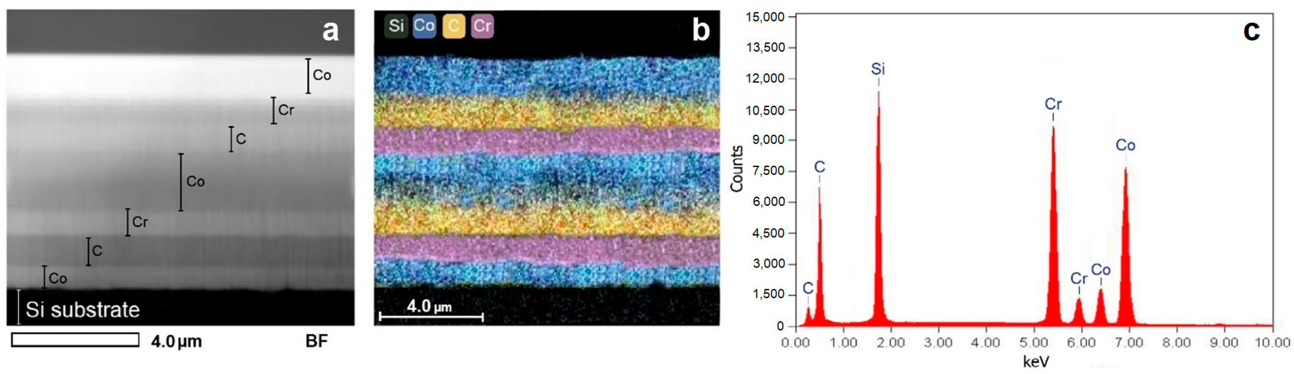
Figure 2 shows the structure and phase composition of the four-layer coating composed of successive Co–C–Cr–Co layers.
Figure 2a presents a BF-TEM image that clearly reveals the multilayer architecture, consisting of four distinct layers, each approximately 1 µm thick. The sharp interfaces between the layers indicate stable deposition conditions and the absence of significant interlayer diffusion.
Figure 2b presents a STEM-EDS elemental mapping, illustrating the spatial distribution of the primary elements (Co, Cr, and C). Each element is distinctly confined to its respective layer, confirming the successful formation of the intended layer compositions with minimal interlayer mixing.
Figure 2c displays the results of X-ray diffraction analysis, revealing diffraction peaks corresponding to crystalline phases of Co and Cr, indicative of the nanocrystalline nature of the metallic layers. A distinct peak near ~1.7 keV corresponds to silicon, originating from the crystalline structure of the substrate. The presence of carbon suggests the incorporation of graphite-like or amorphous carbon within the coating. Notably, the absence of peaks corresponding to oxides or other secondary phases confirms the high purity of the coating and the lack of significant oxidation.
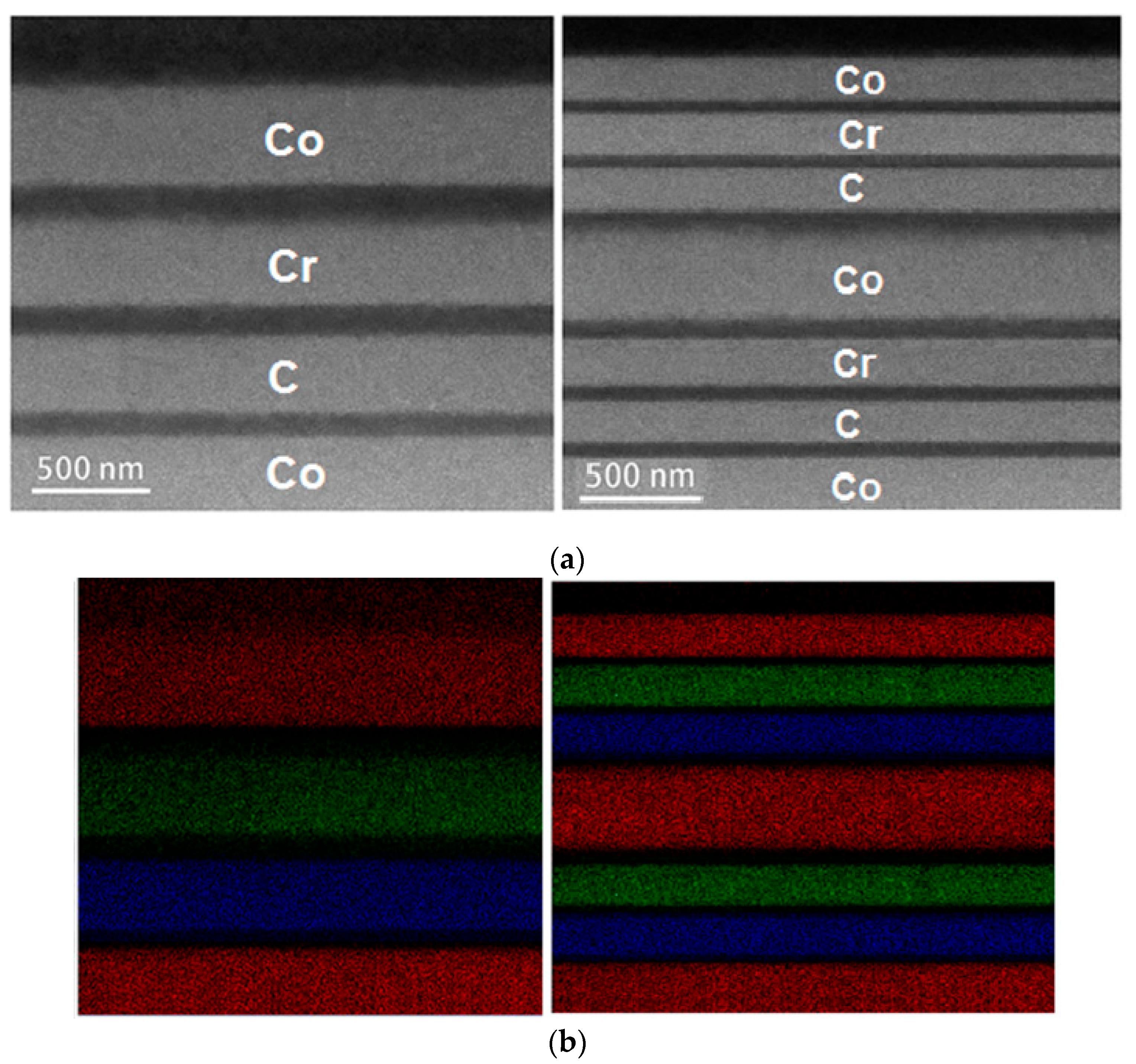
Based on transmission electron microscopy and phase analysis data (
Figure 3), the structural and phase characteristics of the eight-layer Co–Cr–C coating are described. The bright-field (BF) TEM image reveals a well-defined multilayer morphology composed of eight alternating layers deposited under similar conditions, each exhibiting consistent thickness. The elemental distribution map for chromium (Cr K line) confirms its localization within specific layers, indicating the periodic alteration of chromium-rich and chromium-deficient (presumably cobalt- or carbon-rich) regions within the coating structure. X-ray diffraction analysis further confirms the presence of metallic Co, metallic Cr, and free-state carbon in the coating. The observed diffraction peaks correspond to the crystalline phases of Co and Cr, suggesting the retention of their metallic crystalline structures during deposition. Carbon-related peaks likely correspond to amorphous or partially crystallized carbon. A distinct silicon peak is also present, attributable to the crystalline silicon substrate.
The obtained data indicate a coherent multilayer architecture featuring alternating magnetic and dielectric layers, which creates an impedance gradient and promotes interference-induced suppression of microwave radiation, thereby enhancing the microwave-absorbing performance of the coating.
Moreover, modeling the absorption behavior of multilayer Co–C–Cr radio-absorbing coatings as a function of electromagnetic radiation frequency is essential for several reasons, encompassing both fundamental research and practical applications in electromagnetic interference (EMI) shielding. This modeling is particularly important for optimizing the radio-absorbing properties—specifically, understanding how each individual layer contributes to wave interference, reflection, and absorption. It also allows for a comparative assessment of the performance of four- and eight-layer structures, highlighting how increasing the number of layers affects not only the total thickness but also the overall electromagnetic response of the system.
A more detailed structural analysis of the interlayer boundaries based on the STEM-EDS mapping is presented in
Figure 4, where the elemental concentration profiles (Co, Cr, C) are plotted along the direction normal to the layers.
The analysis of the elemental profiles showed that the width of the transition zones between layers did not exceed 20–30 nm, corresponding to a compositional gradient of less than 5% in mass fraction—an indicator of low interlayer diffusion. In addition, a boundary sharpness criterion was applied based on the calculation of intensity gradients at the interfaces using bright-field TEM (BF-TEM) images. The measured contrast variations within ≤10 nm further confirmed the presence of well-defined interfaces. These data allow the coating structure to be objectively characterized as a multilayer system with clearly delineated boundaries and minimal interfacial mixing.
For both the four-layer and eight-layer coatings, diffraction peaks corresponding to the metallic phases of cobalt (hexagonal structure, planes (100), (101), (110)) and chromium (cubic structure, planes (110), (200)) were identified. The carbon peaks appeared weak and broad, indicating a predominantly amorphous state of the carbon layers.
Additionally, the average crystallite sizes were calculated using the Scherrer equation: for Co, the average size was approximately 12–15 nm; for Cr, around 10–13 nm. These values confirmed the nanocrystalline nature of the metallic layers. The broad and low-intensity peaks, especially under grazing incidence, further supported the amorphous–crystalline character of the film.
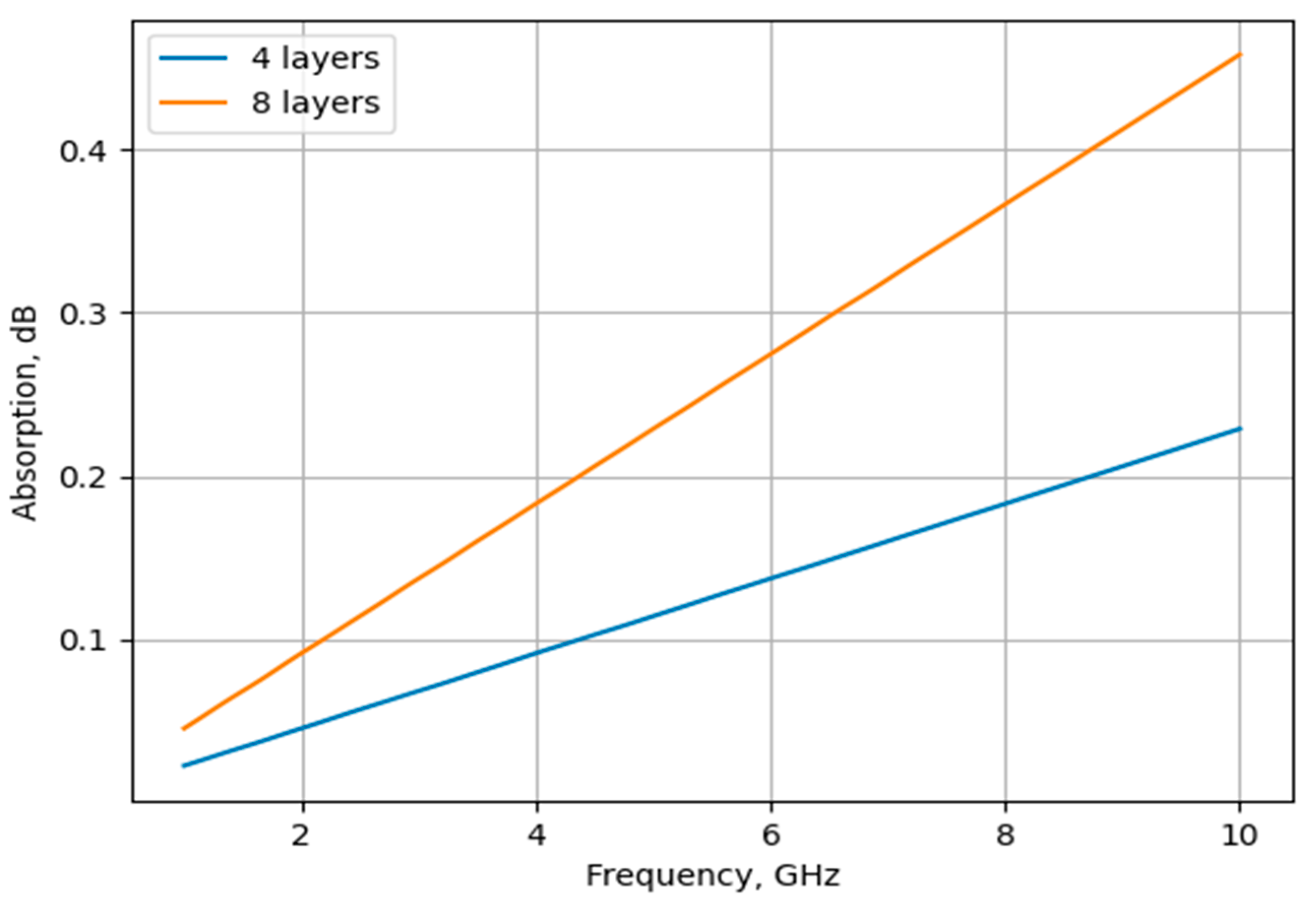
Thus, in
Figure 5, the absorptions of the four- and eight-layer coatings are modeled depending on the number of layers. The modeling was based on a one-dimensional electrodynamic absorption model of the multilayer structure, taking into account the complex dielectric permittivity of each layer. The parameters used were obtained from the literature and experimental estimates. The input data for the simulation are summarized in
Table 2.
The thickness of each layer was set according to SEM measurements, approximately 1 μm, including interface zones of 20–30 nm. The wave number was calculated using Equation (2), attenuation was determined through the imaginary part of the wave number (Equation (3)), and absorption was then evaluated by Equation (4) within the frequency range of 8–12.5 GHz. The boundary conditions assumed normal incidence of a plane wave on the coating surface, with an initial impedance load of 50 Ω (air). Reflection and transmission were calculated iteratively at each layer interface.
The differences between the theoretical and experimental S11 reflection curves can be explained by several factors: (1) non-ideal layer thickness in real samples (±0.1 μm), (2) the influence of the porous substrate, and (3) possible inhomogeneity of the amorphous layers and local diffusion. Additionally, the theoretical model did not account for edge effects and 3D factors (such as surface roughness and interface overlap), which may shift resonance frequencies and reduce the depth of reflection minima. Nevertheless, the qualitative agreement of the absorption bands and the nature of the resonance minima confirm the validity of the model. A comparison of the experimental and theoretical data is presented in
Table 3.
The use of complex dielectric permittivity and its associated relations for absorption calculations is a standard and widely accepted approach in the modeling of multilayer metamaterials. This method allows for an accurate representation of key physical processes—such as dispersion and losses—without the need for excessively complex models, and the results show good agreement with experimental data.
The graph illustrates the dependence of the material’s absorption coefficient on frequency for coatings composed of 4 and 8 layers. It is evident that increasing the number of layers results in higher absorption across the entire frequency range. The curve for the 8-layer structure consistently lies above that of the 4-layer structure, indicating enhanced electromagnetic wave absorption. This improvement is likely due to the formation of a gradual impedance transition facilitated by layers with varying dielectric and magnetic properties, which reduces reflection and increases energy dissipation. Each layer partially reflects and absorbs incoming electromagnetic waves, and the reflected waves interact, leading to interference-based attenuation. Consequently, the strategic combination of layers with different properties enhances broadband absorption.
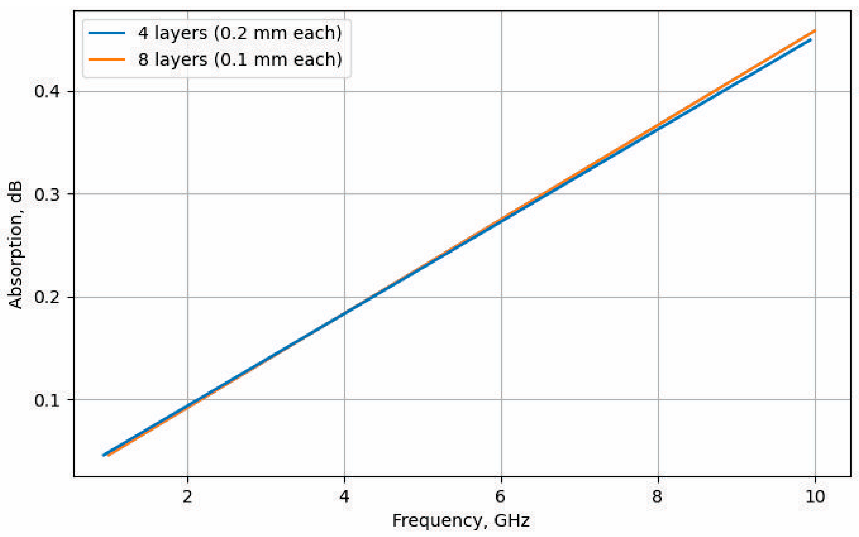
Figure 6 presents absorption as a function of frequency for coatings with the same total thickness but different numbers of layers (4 and 8). In this case, the two curves are much closer, indicating that when the total thickness is fixed, the number of layers has a less significant effect on absorption. As seen from the graphs, absorption primarily depends on the thickness of the layers rather than the total number of layers.
Thus, multilayer magnetron coatings offer multiple functional advantages. One of the key benefits is improved adhesion, as each individual layer can enhance bonding between the substrate and subsequent coatings. The multilayer architecture also reduces the likelihood of defects, cracks, and delamination, resulting in a more durable and mechanically robust coating. Another important aspect is the predictability of the structure. Multilayer designs enable precise control over the composition and structure of each layer, facilitating the tailoring of targeted performance characteristics—such as magnetic, electrical, and mechanical properties. This level of control allows for accurate prediction of the material’s behavior and its impact on device performance. Furthermore, magnetron sputtering technology enables the deposition of thin films with specified thickness and composition. In a multilayer configuration, it becomes easier to fine-tune the coating’s properties by adjusting the deposition parameters for each layer individually. This contributes to greater structural stability and reproducibility, which are essential for modern advanced materials and functional devices.
The increase in absorption with a greater number of layers (
Figure 5) is associated with the formation of a graded impedance profile and an increased number of interfaces, where partial reflection and interference-induced attenuation of the electromagnetic wave occur. These processes enhance field attenuation within the structure, especially when alternating layers with contrasting magnetic and dielectric properties (Co ↔ C ↔ Cr) are used. The transition from four to eight layers results in a smoother variation in wave impedance across the thickness and broadens the range of effective absorption.
To assess the statistical significance of the observed differences, a series of repeated measurements was conducted (n = 3 for each architecture). The average S11 reflection coefficient in the range of 8.2–12.4 GHz was –3.1 dB ± 0.3 dB for the four-layer coating and –2.3 dB ± 0.2 dB for the eight-layer coating. This indicates a statistically significant difference (p < 0.05) in overall efficiency, with the eight-layer coating showing more uniform absorption and the four-layer structure exhibiting localized resonance minima. This difference enables targeted selection of the coating architecture depending on the application—resonance-based shielding or broadband EMI protection.
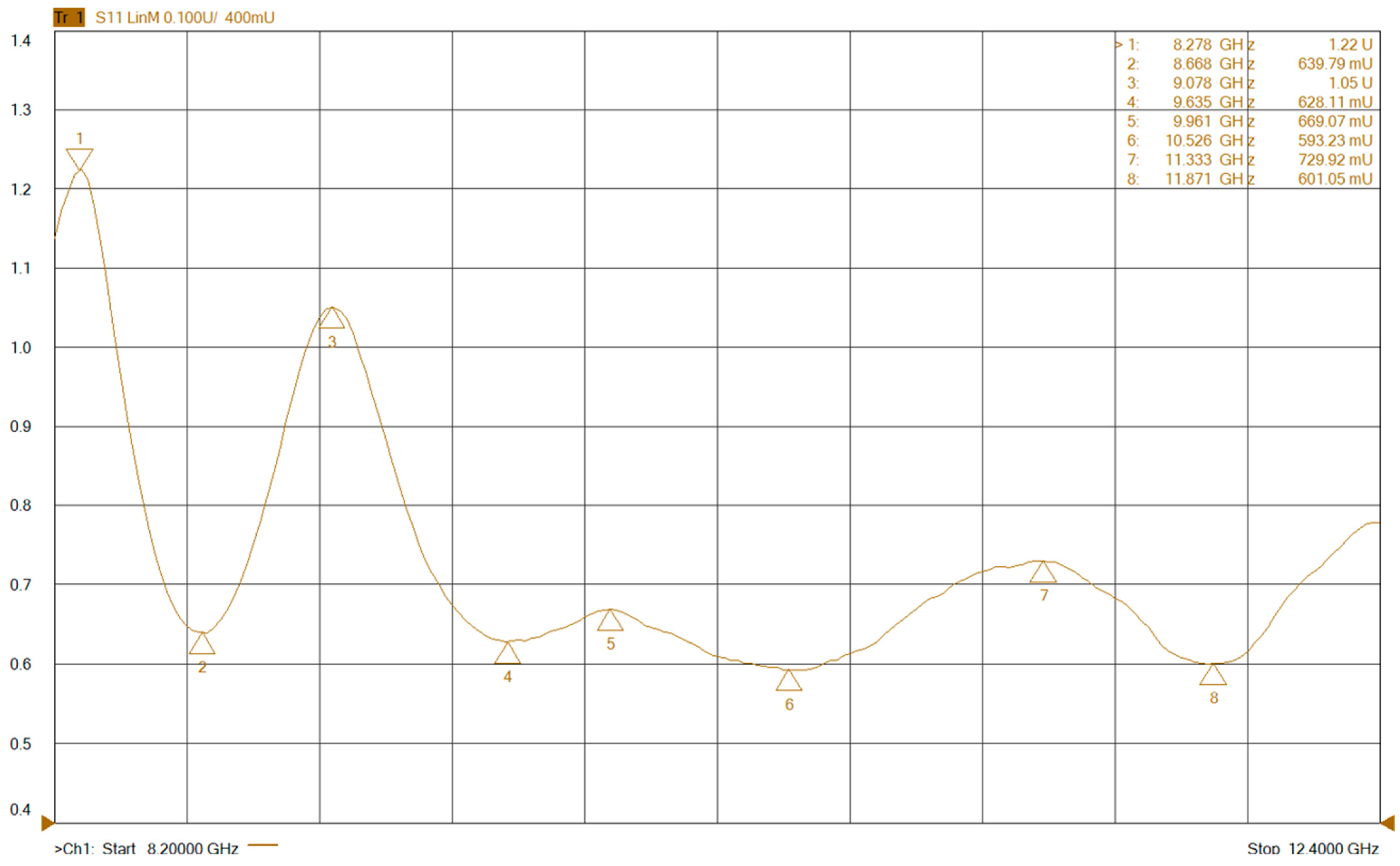
Figure 7 illustrates the frequency dependence of the reflection coefficient (S11) in linear scale over the 8.2–12.4 GHz range. The S11 parameter quantifies the proportion of the electromagnetic wave reflected from the surface: the lower the S11 value, the higher the wave absorption by the material. An S11 value near 1 indicates total reflection (minimal absorption), whereas a value below 0.5 suggests high absorption efficiency. The graph reveals distinct minima in the reflection coefficient—indicative of maximum absorption—around 9.0–9.5 GHz and 11.0–11.5 GHz. These regions correspond to the optimal performance of the coating in attenuating incident electromagnetic energy. Conversely, local maxima (reflection peaks) are observed at approximately 8.5–8.8 GHz and 10.0–10.5 GHz, where the coating reflects a larger portion of the incident wave and performs less efficiently. Although the coating is not broadband, it exhibits multiple resonance absorption characteristics, which can be advantageous for applications requiring targeted interference suppression at specific frequencies rather than across the entire spectrum.
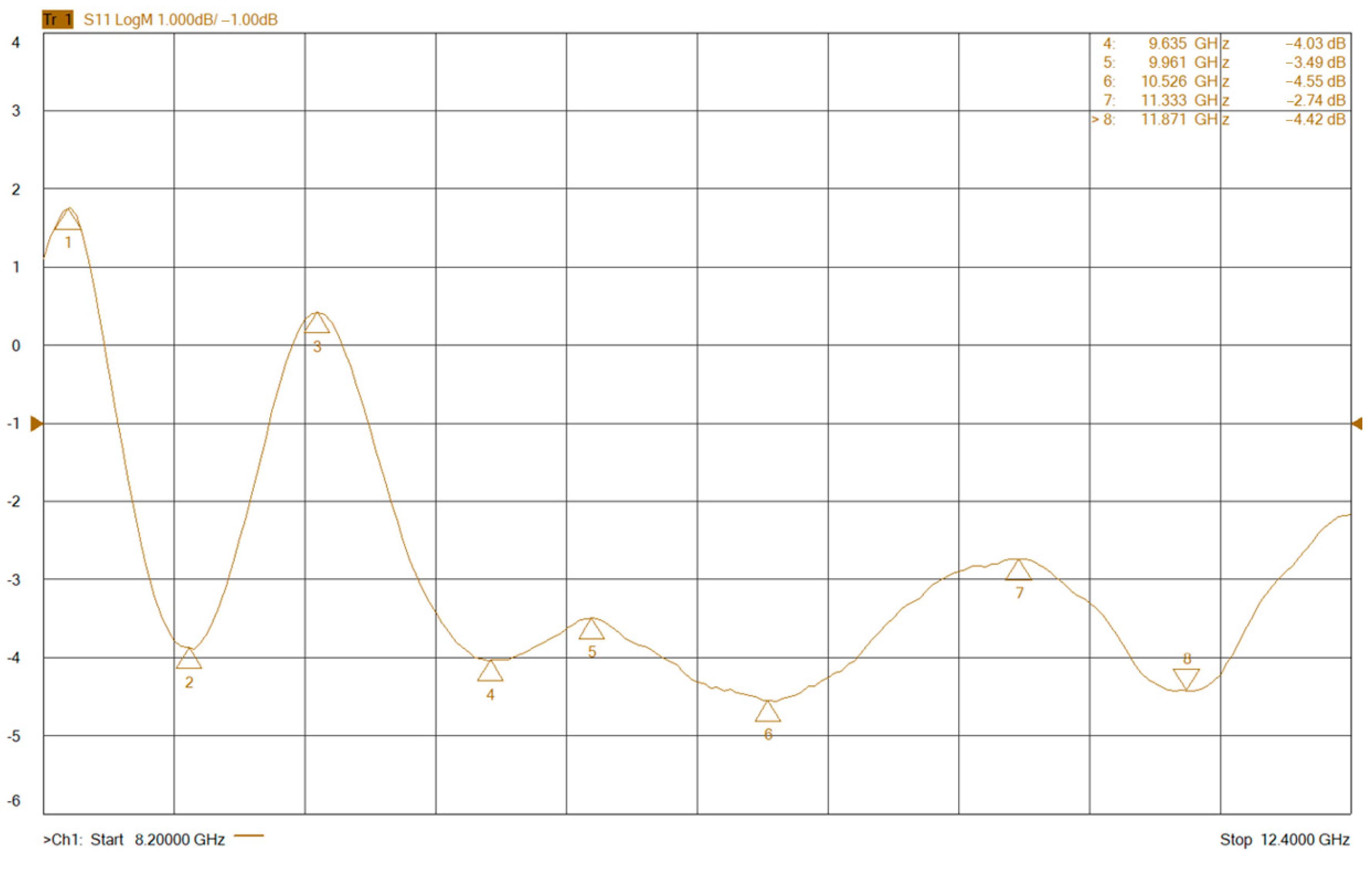
Figure 8 illustrates the frequency dependence of the reflection coefficient S11 in logarithmic scale (LogMag) within the range of 8.2–12.4 GHz. The S11 (LogMag) parameter reflects the signal reflection level: the lower the value, the lower the reflection and the more efficient the absorption of electromagnetic energy. When S11 > −3 dB, more than 50% of the energy is reflected, while S11 < −10 dB indicates over 90% energy absorption, which is considered highly effective. Several distinct minima are observed in the S11 values (indicating optimal absorption): the first pronounced minimum appears around 8.8 GHz, corresponding to approximately 70% absorption of the incident wave; the next minimum occurs near 9.5 GHz, where absorption improves to about 75%; another significant minimum is seen at around 11.3 GHz, indicating the highest efficiency with roughly 80% absorption. Between these minima, increased S11 values are observed, reflecting reduced absorption efficiency in those frequency intervals.
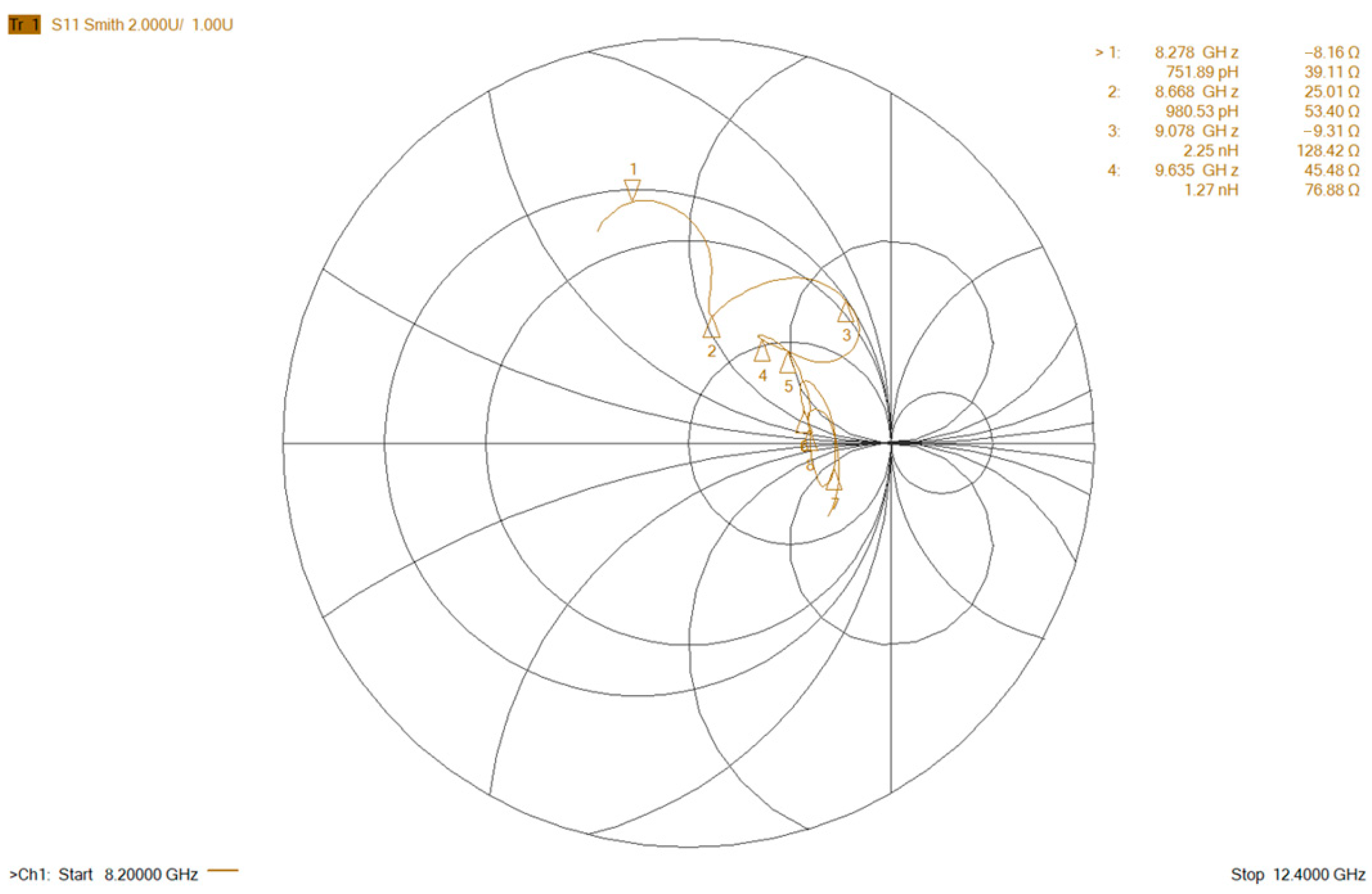
Figure 9 presents a Smith chart, which is used to analyze the impedance of the coating as a function of frequency. The chart includes reference circles representing constant values of resistance and reactance. It depicts how the impedance varies within the 8.2–12.4 GHz range. The horizontal axis represents the real part of the impedance (resistive component), while the vertical axis indicates the imaginary part (reactive component), which can be inductive or capacitive. The center of the chart (normalized impedance = 1) corresponds to perfect matching with the system’s characteristic impedance, typically 50 ohms. When the impedance point is closer to the center, reflection is minimized, indicating more efficient performance of the coating. Conversely, points farther from the center indicate increased reflection and reduced electromagnetic absorption efficiency.
Analysis of the Smith chart for the four-layer coating enables a detailed assessment of the impedance behavior at various frequencies. The accompanying table lists the measured impedance values across the frequency range. In the 8.2–8.6 GHz interval, the impedance exhibits an inductive reactance, with the resistive component ranging from 25 to 39 ohms, indicating a deviation from the optimal 50-ohm matching. In the 9.0–9.6 GHz range, the coating demonstrates capacitive characteristics, with the resistive component increasing to 128 and 76 ohms, further highlighting impedance mismatch.
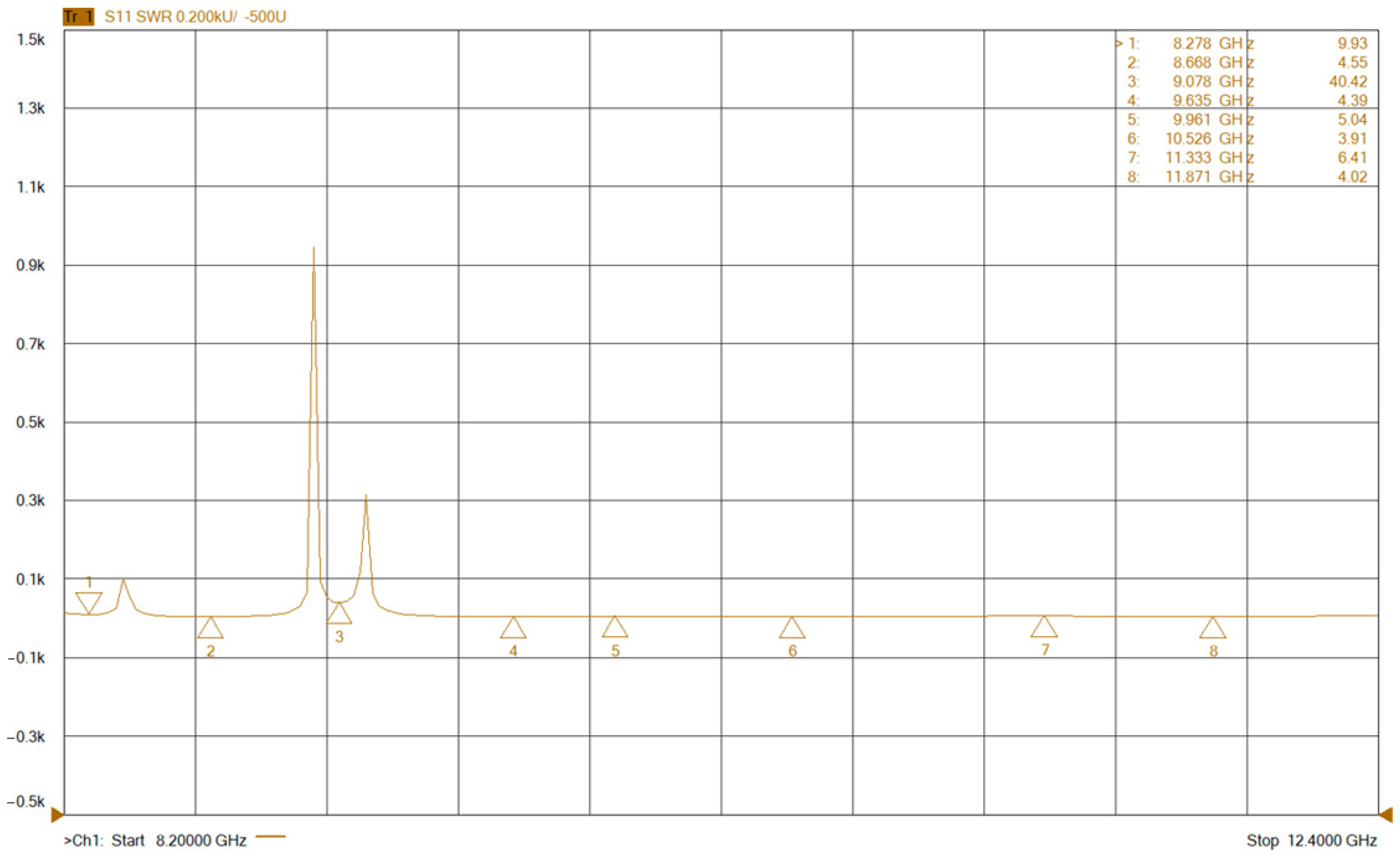
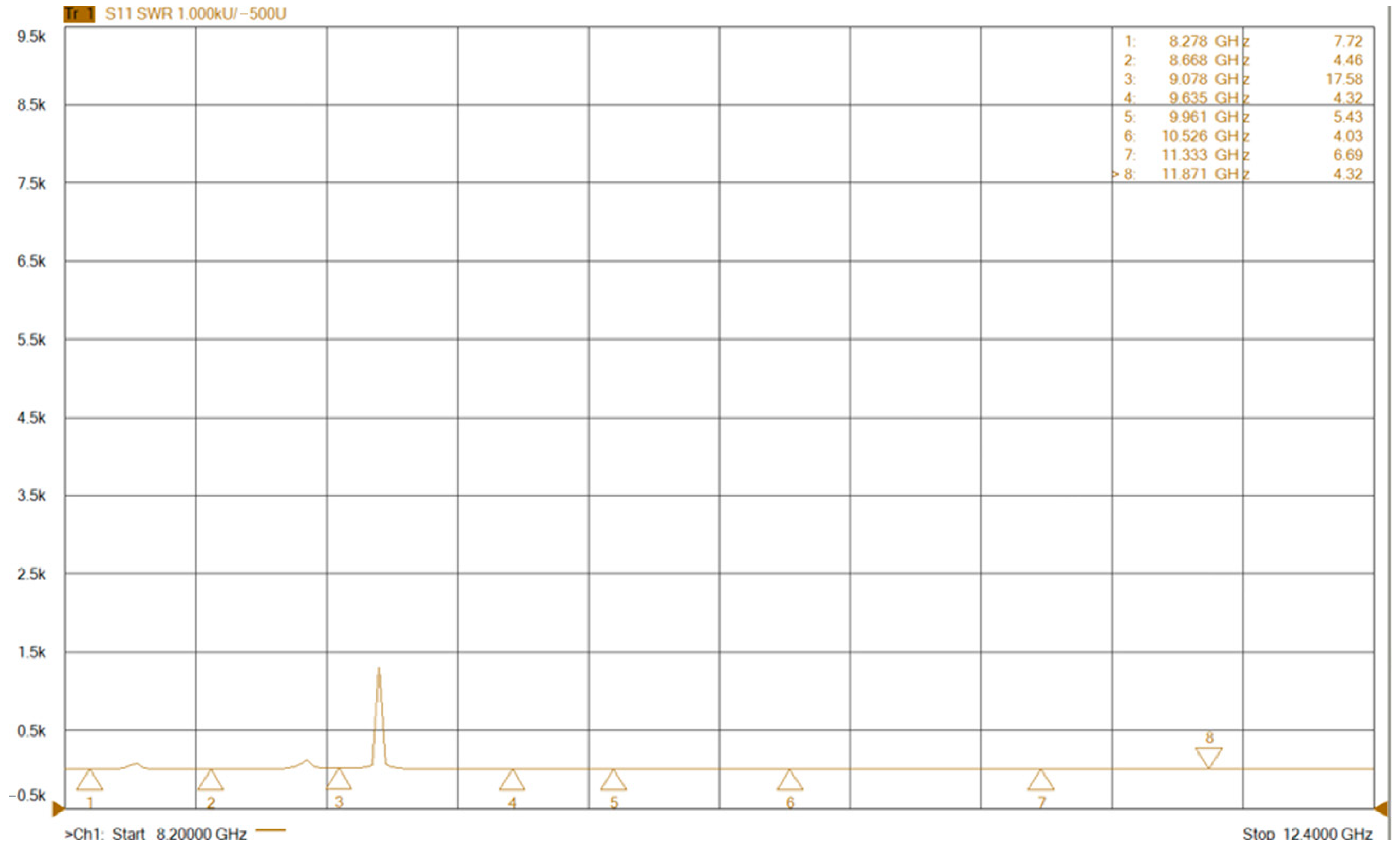
Figure 10 shows the frequency dependence of the standing wave ratio (SWR), which reflects how well the load (in this case, the coating) is matched to the system’s characteristic impedance (typically 50 ohms). An SWR value of 1 denotes perfect matching—i.e., complete absorption of incident electromagnetic waves. Values greater than 1 indicate the presence of reflections, and SWR values exceeding 10 correspond to high reflection levels and poor absorption.
The graph reveals sharp SWR peaks, emphasizing the frequency-dependent nature of the coating. Across a broad frequency range, the SWR remains significantly above 2, indicating non-uniform impedance matching and the narrowband absorption behavior of the coating. A pronounced peak is observed at 9.078 GHz, where the SWR reaches 40.42, signifying strong reflection and minimal absorption. In the 9.5–9.7 GHz range, SWR values also exceed 10, confirming poor impedance matching in this interval. Moderate SWR values (around 4.5) are observed in the 8.6–8.7 GHz region, suggesting partial matching but still with substantial reflection losses. At approximately 11.8 GHz, the SWR decreases to about 4.02, indicating relatively improved matching compared to the peak values.
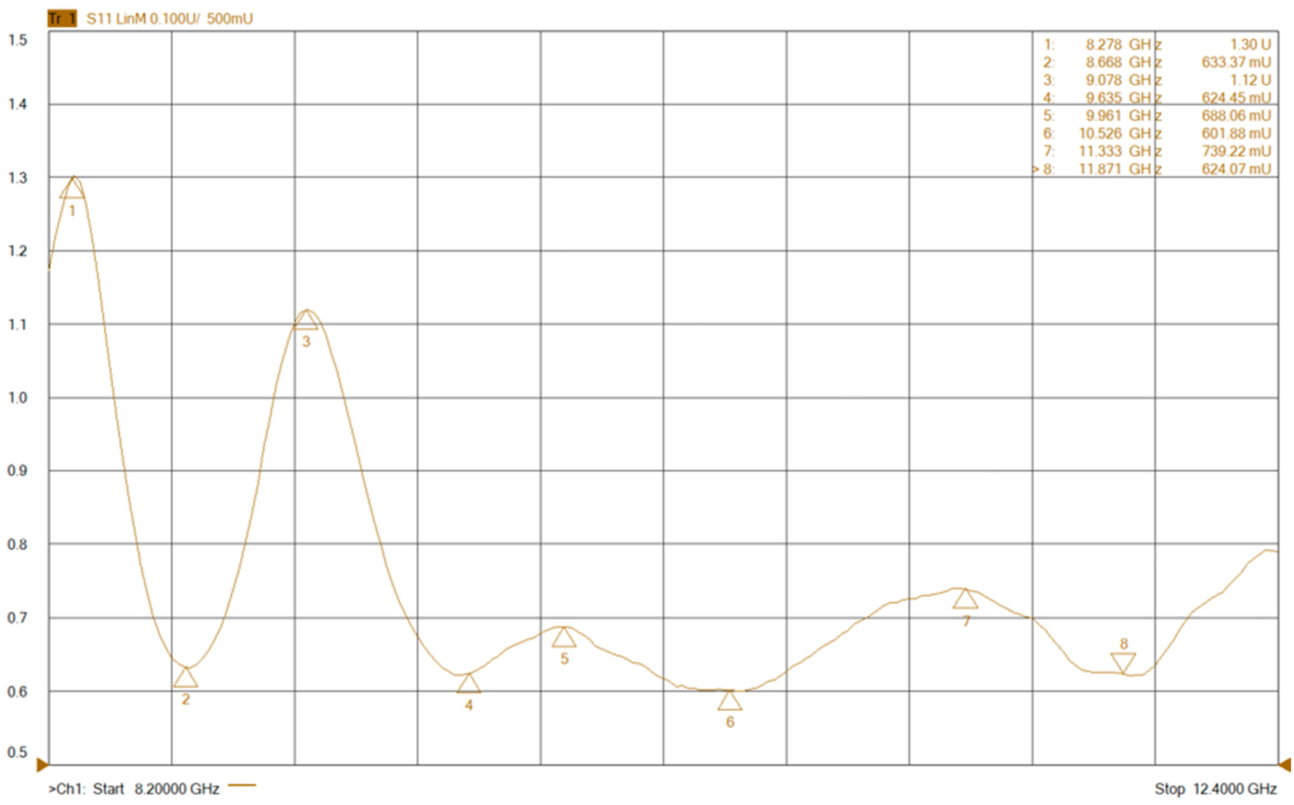
Figure 11 presents the frequency dependence of the reflection coefficient S11 (LinMag) for the eight-layer coating. Several reflection minima are observed, indicating resonance frequencies at which the coating effectively absorbs electromagnetic waves. Notable S11 minima appear at 8.2 GHz, 9.0 GHz (with the strongest absorption), around 10.5 GHz, and 11.8 GHz. In contrast, reflection maxima (corresponding to poorer absorption) are observed in the 8.6–9.0 GHz and 11.0–11.5 GHz intervals. Sharp increases in the reflection coefficient (S11 ≈ 1.2) are also present, signifying high levels of wave reflection and indicating that the coating does not provide uniform absorption across the entire frequency range.
The eight-layer coating shifts the S11 minima toward the higher frequency range (8.0–11.8 GHz); however, the minimum values do not reach the lower levels of 0.3–0.4 observed in the four-layer coating. While the four-layer structure exhibits pronounced narrowband minima and achieves lower S11 values at specific frequencies, the eight-layer coating demonstrates a more uniform absorption profile across the spectrum. This suggests an improvement in bandwidth performance but a reduction in peak absorption efficiency. On average, the eight-layer coating provides smoother transitions between minima and maxima, yet S11 values in some frequency intervals are higher compared to the four-layer structure. The deeper minima in the four-layer coating indicate better impedance matching at certain resonant frequencies, although its performance deteriorates outside those narrow bands.
Figure 12 displays the frequencies and corresponding S11 values: high reflection (undesirable for absorption) at 8.278 GHz (2.26 dB) and 9.678 GHz (0.97 dB) associated with resonance-induced reflections or structural features of the multilayer sample and low reflection (desirable for absorption) at 8.668 GHz (−3.97 dB), 9.035 GHz (−4.11 dB), 9.361 GHz (−3.23 dB), 10.526 GHz (−4.44 dB), and 11.871 GHz (−4.11 dB) corresponding to significant reflection loss, indicating efficient absorption of electromagnetic energy. Deep reflection minima (such as −4.44 dB at 10.526 GHz) highlight frequencies where wave energy is effectively absorbed by or transmitted into the material. These absorption peaks likely result from resonance effects, while the maxima may be attributed to interfacial reflections between distinct layers in the multilayer structure.
The oscillatory pattern of the S11 curve supports the presence of complex multilayer interference phenomena. This behavior underscores the potential of such coatings for frequency-selective applications. In practical terms, such as in antennas or EMI shielding materials, peaks at 8.278 GHz and 9.678 GHz could indicate undesired reflections, while the minima mark preferred operational frequencies (e.g., 8.668, 9.035, 10.526, and 11.871 GHz) due to more efficient absorption. The observed resonance effects confirm the viability of using multilayer designs to tailor and control the reflectivity of functional materials.
It can also be observed that the reflection loss levels differ slightly between the eight-layer and four-layer samples. In certain frequency regions, the S11 LogMag values for the eight-layer sample are lower than those of the four-layer one, indicating improved signal absorption. Both plots feature distinct minima, which correspond to frequencies at which reflection losses are maximized. However, the position of these minimums may shift slightly with an increasing number of layers. This suggests that increasing the number of layers influences the reflection coefficient, potentially reducing the reflected signal level and enhancing the absorption of electromagnetic energy.
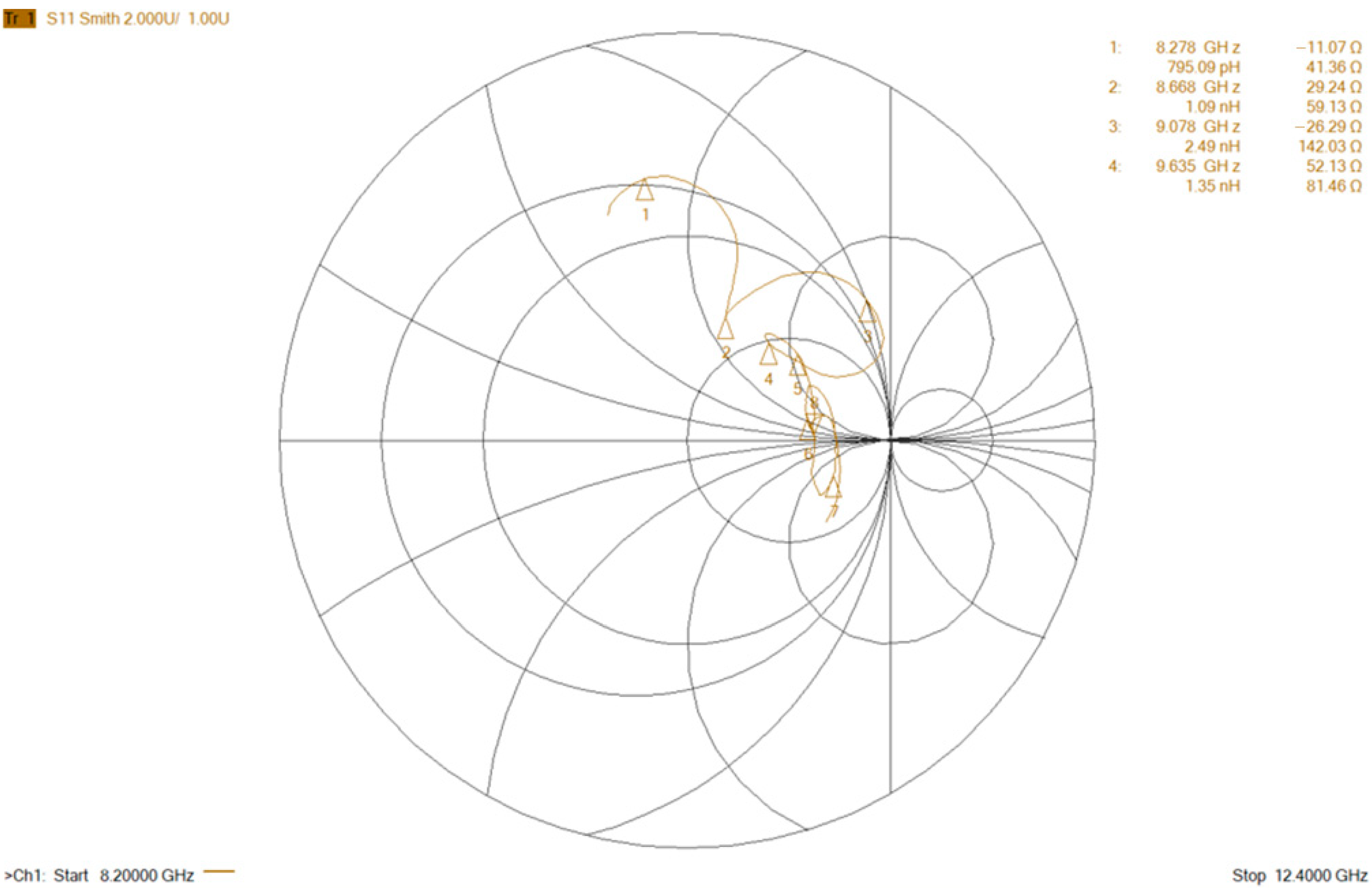
In
Figure 13, at a frequency of 8.278 GHz, the measured impedance is −11.07 Ω, with a corresponding reactance of 795.09 pF. Other measurement points exhibit varying impedance values and reactive components (capacitance or inductance). Negative values of the real part of the impedance (such as −11.07 Ω at 8.278 GHz) may indicate the presence of active elements or non-standard high-frequency effects. The reactive components reflect the capacitive or inductive behavior of the sample. The graph also includes equivalent inductance and capacitance values, derived from the impedance characteristics. At the beginning of the measurement range (8.2 GHz), the impedance is close to zero, indicating good impedance matching. As the frequency increases up to 12.4 GHz, the impedance exhibits a complex, nonlinear dependence typical of multilayer systems with frequency-dependent properties. The simultaneous presence of capacitive and inductive features highlights the complex internal architecture of the sample, which likely consists of alternating conductive and dielectric layers. These interactions contribute to the frequency-selective behavior and must be considered when designing such coatings for EMI shielding or microwave absorption applications.
When comparing the obtained data with
Figure 9 for the four-layer coating, clear differences in impedance behavior are evident. The impedance trajectory of the four-layer sample is more compact and concentrated near the center of the Smith chart, indicating better impedance matching and a simpler reactive profile. In contrast, the eight-layer sample demonstrates a broader distribution of impedance values, reflecting a more complex reactive component. This complexity arises from the increased number of internal reflections and electromagnetic interactions between layers as the number of layers increases.
The diagrams presented in
Figure 9 and
Figure 13 illustrate the movement of the impedance trajectory as a function of frequency: proximity to the center indicates effective matching with the characteristic wave impedance (50 Ω), which is critical for minimizing reflections in microwave devices. Regions where the trajectory moves away from the center correspond to frequencies with high reflection levels.
Negative values of the real part of the impedance, such as −11.07 Ω at 8.278 GHz, may occur due to the complex interaction of capacitive and inductive components within the multilayer structure under resonant conditions. These values do not indicate the presence of active elements but instead reflect phase shifts between current and voltage under standing wave conditions and multiple internal reflections.
Such behavior is typical for metamaterials and frequency-selective surfaces, confirming the potential of the coating as a filter or absorber with a defined frequency band. Therefore, analysis using Smith charts enables not only the evaluation of impedance matching but also the prediction of the effective absorption frequency ranges depending on the coating architecture.
Figure 14 displays the frequencies and corresponding reflection coefficient values. The most notable frequency points are 8.278 GHz—7.72, 8.068 GHz—4.46, 9.078 GHz—17.58 (maximum reflection), 9.035 GHz—4.32, 9.961 GHz—5.43, 10.526 GHz—4.03, 11.333 GHz—6.69, and 11.871 GHz—4.32. Several prominent reflection peaks are observed, indicating potential resonance frequencies within the system. The highest reflection value at 9.078 GHz is likely linked to strong internal resonances within the multilayer structure. Other significant peaks, such as at 8.278 GHz (7.72) and 11.333 GHz (6.69), may also be attributed to constructive interference caused by specific layer arrangements. Conversely, relatively lower values (below 5) at 8.068 GHz, 9.035 GHz, 10.526 GHz, and 11.871 GHz suggest improved impedance matching and more efficient wave transmission at those frequencies. These lower S11 values may correspond to frequencies where destructive interference or impedance matching reduces reflection, allowing greater energy penetration into the material. The observed reflection peaks are closely related to the design of the multilayer structure, particularly the presence of layers with differing dielectric permittivities and multiple internal interfaces. The highest reflection at 9.078 GHz may correspond to a condition where constructive interference enhances wave reflection due to impedance mismatches across the layers. Such multilayer systems can behave as frequency-selective surfaces, exhibiting selective transmission and reflection characteristics depending on frequency. Strong S11 spikes at certain resonant frequencies likely result from the superposition of reflected waves at specific material boundaries. This emphasizes the importance of precise control over layer thicknesses and dielectric properties to minimize impedance mismatches and suppress undesirable reflections. Overall, minimal S11 values (e.g., at 10.526 GHz) point to effective electromagnetic wave transmission and absorption, while high S11 values highlight frequencies where impedance mismatches degrade performance.
Based on the obtained results, it can be concluded that the sample performs poorly in terms of signal absorption around 9.078 GHz, where strong reflection is observed. However, when interpreted in the context of frequency filtering, the structure behaves like a frequency-selective surface, reflecting certain portions of the spectrum while allowing other frequencies to pass through.
The sharp minima of the reflection coefficient (S11) at frequencies 8.8 GHz, 9.0–9.5 GHz, and 11.3 GHz are caused by interference-induced cancellation of the electromagnetic wave at the interfaces between layers with different dielectric and magnetic permeabilities. These interfaces, confirmed by STEM-EDS, form an impedance gradient that facilitates effective signal attenuation. The presence of alternating nanocrystalline Co and Cr layers (with high magnetic and conductive activity) and amorphous C (with pronounced dielectric losses) enhances absorption through resonant and multiple reflections. Conversely, the S11 maxima correspond to frequencies where impedance mismatches at interfaces dominate and reflection is prevalent.
Analysis of the SWR and Smith impedance diagrams further confirms the presence of resonance effects, and their frequency positions correlate with the layer thicknesses and overall coating architecture. Thus, the features observed in the S11 and LogMag plots reflect the complex frequency-dependent structure of the multilayer system and are explained by its phase composition and morphological configuration.
The main contribution to enhanced absorption efficiency comes from the impedance gradient, which arises from the alternating layers with different dielectric and magnetic properties (e.g., Co—high magnetic permeability, Cr—moderately conductive, and C—dielectric with high loss). At the interfaces between such layers, smooth transitions in wave impedance are created, gradually shifting from air toward the inner layers of the coating. This reduces abrupt reflection at the “air–material” interface and facilitates deeper wave penetration, where the energy gradually attenuates through multiple internal reflections and interference.
Each interface acts like a semi-transparent mirror, partially reflecting and partially transmitting the wave. Reflected waves within the coating can interfere with incident waves, causing destructive interference and further reducing overall reflection. This mechanism is characteristic of impedance transformers commonly used in radio frequency engineering for impedance matching. In multilayer microwave absorbers, a similar effect is achieved by carefully selecting layers to provide wave matching throughout the coating’s thickness. As a result, energy is not reflected but scattered and absorbed within the material—primarily due to dielectric losses (in C layers) and magnetic losses (in Co and Cr layers). The impedance gradient and layer design provide both reduced reflection and efficient dissipation of electromagnetic energy.
Thus, increasing the number of layers in the coating leads not only to greater total thickness but also to a larger number of interfaces with contrasting electromagnetic properties. These interfaces (e.g., Co–C and C–Cr) act as secondary scatterers, causing multiple internal reflections. Due to destructive interference of reflected waves and the formation of standing waves at the microscale, part of the energy is effectively suppressed, reducing the overall reflection coefficient.
An additional contribution comes from the contrast between the phase states of the amorphous carbon layers and the nanocrystalline metal layers. Amorphous regions have a high density of local vibrational modes and contribute to dielectric losses, while the nanocrystalline Co and Cr layers (with crystallite sizes of 10–15 nm) contribute to magnetic losses and microscopic scattering due to magnetic permeability inhomogeneities.
Moreover, slight interlayer diffusion (transition zones ~20–30 nm) creates a continuous impedance profile, smoothing reflections between layers and improving wave penetration into the material. This is especially important in the eight-layer architecture, where the structure approaches that of a gradient metamaterial with quasi-continuous property variation across the thickness. Collectively, these effects broaden the effective absorption bandwidth and provide conditions for broadband operation without sharp performance degradation at specific frequencies.
Analysis of the influence of layer thickness, phase composition, and the ratio of amorphous to crystalline regions on electromagnetic wave absorption shows that layer thickness directly affects interference effects and the depth of resonance minima. At a thickness of about a quarter of the wavelength (λ/4) in a given medium, conditions for destructive interference of reflected waves are met, resulting in a sharp reduction in the reflection coefficient (S11). Experimentally, it was found that ~1 μm thick layers correspond to resonances in the 8–12 GHz range. Increasing the total thickness of the structure (as in the eight-layer coating) leads to absorption band broadening due to accumulated phase shifts across a greater number of interfaces.
Phase composition determines the balance between magnetic and dielectric losses. The nanocrystalline phases of Co and Cr provide magnetic losses (domain resonances, hysteresis), especially in the microwave range. Their presence was confirmed by XRD analysis (Co and Cr peaks, crystallite sizes of 10–15 nm). These phases act as microscopic scatterers, enhancing attenuation through μ inhomogeneity.
Finally, amorphous carbon layers contribute significantly to dielectric losses, especially at higher frequencies, due to the lack of long-range order and the presence of numerous localized states. The amorphous structure enables more uniform energy absorption and reduces the likelihood of sharp resonant reflection peaks. Additionally, the boundaries between amorphous and crystalline regions serve as zones of micro-reflection and diffusion, further reducing reflection.
Thus, the optimal combination of thin layers with controlled phase states and alternating amorphous and crystalline phases ensures efficient electromagnetic energy absorption over a wide frequency range, highlighting the importance of comprehensive control over the morphology and structure of coatings when designing microwave-absorbing materials.
A brief comparative analysis of the properties of the most well-known and widely used coatings is presented in
Table 4, showing the advantages and limitations of Co–C–Cr coatings compared to other established microwave-absorbing materials.
Thus, the Co–C–Cr coatings demonstrate a balanced combination of magnetic and dielectric losses, architectural flexibility, and good thermal stability, outperforming purely dielectric counterparts in terms of efficiency within the microwave frequency range. Compared to graphene- or ferrite-based systems, Co–C–Cr coatings offer a narrower bandwidth, but they are superior in terms of scalability, cost-effectiveness, and morphological reproducibility. The investigated system holds strong potential within the class of mid-band multilayer microwave-absorbing materials, particularly for applications that require structural control, stability, and resonance-based reflection management.
4. Conclusions
The conducted study confirmed the promising potential of Co–C–Cr multilayer coatings fabricated via magnetron sputtering for application as microwave-range electromagnetic wave absorbers. The primary objective was to compare the structural and electrodynamic properties of four- and eight-layer systems and to evaluate the impact of multilayer architecture on the electromagnetic behavior of the coatings.
The conducted modeling showed good agreement with the experimental data. It was established that the magneto-optical properties of the coatings consisting of 4 and 8 layers are nearly identical.
Results of electron microscopy and elemental mapping revealed a well-defined multilayer morphology with clearly distinguishable interfaces and minimal interlayer diffusion, indicating high reproducibility and stability of the deposition process. Chemical analysis confirmed the presence of metallic Co and Cr phases along with amorphous carbon—an optimal combination for providing both magnetic and dielectric losses.
Particular emphasis was placed on the modeling and experimental measurement of the reflection coefficient (S11) and impedance characteristics. It was shown that the multilayer structure contributes to interference-induced attenuation of electromagnetic waves, leading to enhanced absorption efficiency. The four-layer coating exhibited sharp S11 minima at narrow frequency intervals, making it suitable for use in frequency-selective applications. In contrast, the eight-layer coating demonstrated a more uniform response over a broader frequency range, which is advantageous for broadband interference suppression. However, despite the broader absorption bandwidth, the eight-layer structure showed less pronounced minimum S11 values compared to the four-layer coating. This is attributed to the increased complexity of impedance behavior with a higher number of layers, making precise tuning of each interface more challenging. Smith chart and SWR analysis further confirmed that the eight-layer system exhibited reduced impedance matching at certain frequencies despite its general stability. Thus, achieving optimal performance requires not only adjusting the number of layers but also fine-tuning their thicknesses, compositions, and stacking order.
Additionally, the sample’s internal architecture significantly influenced the distribution of reflected and absorbed waves, including the formation of resonant peaks and minimums. This opens up avenues for the deliberate design of frequency-selective surfaces with tailored reflection and absorption characteristics.
Overall, Co–C–Cr multilayer coatings demonstrate high potential for applications in electromagnetic compatibility systems, microwave shielding, antenna technology, and RF filtering. The findings highlight the need for further research focused on structure optimization, interface engineering, and the development of adaptive coatings designed to operate in specific frequency bands. The proposed methodology can serve as a framework for designing next-generation functional materials with engineered electromagnetic absorption and reflection properties, including for EMI protection and advanced coating technologies.
Based on the quantitative analysis of the reflection coefficient (S11), impedance characteristics, and modeling results, it was established that the four-layer Co–C–Cr–Co coatings exhibit pronounced resonance minima (down to −4.4 dB) within narrow frequency ranges (e.g., 9.0–9.5 GHz and 11.3 GHz). This makes them preferable for use in frequency-selective surfaces, RF filters, and antennas where signal suppression at specific frequencies is required. In contrast, the eight-layer coatings provide more uniform absorption over a broader frequency range (8.2–12.4 GHz), albeit with shallower minima, making them promising for broadband EMI shielding, especially in systems designed to protect sensitive electronics from parasitic emissions.
Therefore, for narrowband applications, the simpler four-layer architecture is advisable, while for broadband purposes, the eight-layer structure is more suitable, with further optimization of layer sequencing and thickness.
The DC magnetron sputtering method used in this study is widely applied in industry and can be easily scaled from laboratory setups to semi-automated and full-scale industrial systems. The use of commercially available targets made of Co, Cr, and pressed carbon (from domestic technical-grade carbon P-514) enables implementation without relying on expensive or scarce components. Material consumption is low, and layer thickness is controlled via deposition time and power, making the process economically feasible for mass production.
A series of repeated experiments demonstrated good structural reproducibility: deviations in layer thickness did not exceed ±5%, interfaces remained sharp, and the electromagnetic properties were reproduced within acceptable margins (S11 ±0.2–0.3 dB). This indicates technological reliability and stability of the process, even with multilayer architectures.
The materials used (Co, Cr, amorphous C) are oxidation-resistant and retain their structure at temperatures up to 300–400 °C. Under thermal exposure, some ordering of the amorphous carbon may occur, potentially altering its dielectric properties, but the magnetic properties of the metal layers remain intact. This opens the possibility of using the coatings in moderately heat-loaded systems, including RF shielding in electronic enclosures, microwave components, and filters.
The structure of the coatings can also be adapted to flexible substrates or thermally active elements (e.g., polymers with phase transitions), enabling the creation of adaptive absorbers with tunable characteristics. Furthermore, the coatings can be integrated into frequency-selective surfaces and metasurfaces operating in variable electromagnetic environments or in multiband antenna systems.
In summary, the proposed technology offers a high degree of integration into existing manufacturing processes and is of interest not only from a scientific perspective but also for practical applications, including EMI protection systems, RF devices, and telecommunications equipment.


 ,
, 


