1. Introduction
Since the early isolation of atomically thin layers of molybdenum disulfide (MoS
2) [
1], niobium diselenide (NbSe
2) [
2] and graphite [
3], there has been steady development in the methods to manipulate and control placement of two dimensional (2D) materials. Seemingly austere techniques using adhesive tape and polymers to isolate and transfer these materials [
4,
5,
6,
7,
8,
9,
10] have driven recent research into surprising new directions. For instance, combining isolated materials into heterostructures opens almost limitless possibilities in device properties and functionality [
11]. Intimate contact between two materials with similar lattice constants reveals reconfiguration of the electronic band structure of these materials as a result of a Moire superlattice [
12]. Recently, the ability to precisely rotate and align materials has led to the unexpected observation of superconductivity in these heterostructures [
13,
14].
Of the many techniques developed thus far [
10,
15], the so-called van der Waals pick up method [
7,
9,
16,
17] is preferable in the construction of heterostructures because the layers are not directly exposed to polymers during stacking, resulting in clean interfaces. A noticeable drawback of the technique is a reliance on thin layers of polycarbonate (PC) or polypropylene carbonate (PPC) that must be mixed and prepared, spin-coated or applied to a glass slide before use. In our use of PPC, there is noticeable fatigue of the thin film after many (>5) stacking sequences that can lead to time consuming failure in fabrication from flake cracks, folds and unexpected stack transfers before completion.
Recently, it has been shown that commercially available nitrocellulose polymer solution (nail polish) can be used to pick up 2D material flakes [
18]. Rebollo et al. additionally showed that these flakes and simple heterostructures can then be transferred to any substrate or trench to create suspended structures and cavities. These developments have prompted our interest in using nail polish to construct heterostructures in a modified van der Waals pick up technique.
Building on these recent results, we present a heated technique to assemble and transfer van der Waals heterostructures using common nail polish. We show that 2D materials can be picked up from Si/SiO2 substrates, stacked by van der Waals forces, and transferred by a high temperature melt of the nail polish. Nail polish is a favorable alternative to thin polymer films used in previous van der Waals pick techniques. Whereas PC and PPC films must be mixed a carefully prepared before use, a simple drop of cured nail polish suffices to assemble multi-material (greater than 5 layer) heterostructures without noticeable polymer fatigue. We compare several clear nail polish brands and find that Revlon Nail Enamel, Clear 771 stands out in terms of stability and stacking characteristics. Finally, to demonstrate the feasibility of our approach, we fabricate two top-gated devices and report their electronic properties.
2. Assembly and Transfer of Van der Waals Heterostructures
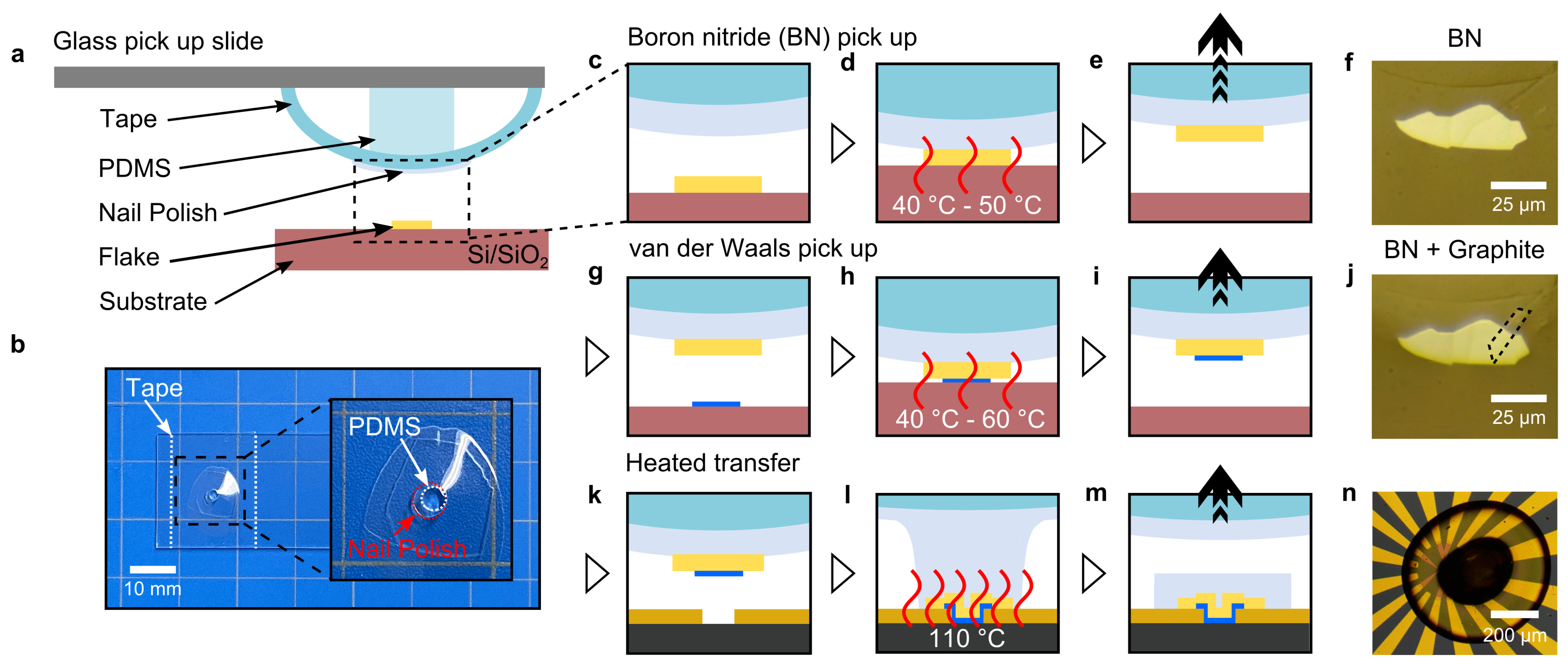
An overview of our technique is shown in
Figure 1. A glass pick up slide (side model shown in
Figure 1a and a top view photograph of one in
Figure 1b) is prepared in the following manner. A small (roughly 3 mm in diameter and 1 mm tall) cylinder of polydimethylsiloxane (PDMS, Dow Corning Sylgard 184, Midland, MI, USA) is created using a biopsy punch. This cylinder is placed at the end of a glass microscope slide and a piece of transparent tape is placed over the cylinder to secure it in place. The PDMS creates a convex surface which can be used to precisely control the contact area between the pick up slide and the substrate surface. Next, a drop of nail polish (Revlon Nail Enamel, Clear 771, New York, NY, USA) is extracted from the bottle using a toothpick or a sharp piece of solder wire. The drop is placed on the surface of the tape at the apex of the PDMS cylinder, most favorably spreading out over the diameter of the cylinder. The slide is then baked on a hot plate, nail polish side up, in ambient conditions at 90 °C for 5 min. This hardens and cures the nail polish, creating a solid sticky surface for flake pick up. We note that slides can be prepared without the PDMS cylinder and only with a single drop of nail polish (similar to Rebollo et al. [
18]) that is hardened on a hot plate. The heated stacking is not ideal however (see the
Supplementary materials for details, Figure S1) because a large deformation of the microstamp occurs with pick up. The nail polish can be reflowed on a hotplate but the large deformation causes problems for complex multi-material stacks.
This aspect of the slide preparation simplifies the process and leads to higher yield when compared with the original van der Waals method using a thin PPC (Sigma Aldrich, St. Louis, MO, USA) film [
7]. In the original technique, PPC films are created by first mixing 3 g of PPC pellets with 22 mL of anisole. The solution is thoroughly mixed over a hotplate at 50–60 °C for six hours. The solution is then filtered through a 0.5 micron mesh and stored for use. To prepare a thin film, the mixture is then drop cast onto a silicon chip, spun at 2000 rpm, and baked at 90 °C for 2 min. Then, using a piece of adhesive tape with a 5 mm hole in the middle, the film is picked up and placed on top of the PDMS/tape cylinder described above. The transfer is done by hand and this results in a significant fraction (≈30%) of the slides that are not usable due to folds and bubbles in the transferred film. The nail polish method both simplifies this process and increases the yield of prepared slides.
After slide preparation, the first 2D material flake can be picked up. In this example, and for many of our stacks, the first flake is a boron nitride (BN) flake. This material provides an atomically flat surface for the subsequent pick up of other 2D materials using the van der Waals force. We have found though that other materials, like graphene and graphite, can be picked up in the first sequence if required for a particular application.
To pick up the first BN flake, the pick up slide is mounted into a custom adapter attached to a probe station micromanipulator (3-axis Wentworth laboratories micro-positioner) allowing precise control over x-y-z axes and bulk BN material is exfoliated onto Si/SiO
2 substrates using adhesive tape [
3]. The flake of interest is aligned under the pick up slide using a microscope. The slide is then lowered slowly, taking care to not inadvertently touch the surface. To find the contact point of the nail polish, the slide is lowered to a location near the target BN flake. Once the contact point is ascertained, the slide is raised slightly (≈100 μm) and aligned just to the side of the target flake (
Figure 1c. The slight misalignment between the contact point and the target flake is so that after the nail polish is brought into contact with the substrate surface, an increase in stage temperature (
Figure 1d) can be used to controllably and steadily cover the flake with the nail polish. The typical temperature used for this step is around 40 °C to 50 °C. Once the flake has been completely laminated with nail polish, the temperature is lowered back to 40 °C. The slide is then raised in one continuous and swift motion to “pop” the BN flake from the surface of the substrate (
Figure 1e). A representative optical image of a BN flake on a pick up slide after pick up is shown in
Figure 1f.
Following pick up of the first flake, the slide is placed on a hot plate at 90 °C for 1–2 min to reflow the nail polish. This step smooths out the nail polish surface and reduces any distortions in the thin film that may have appeared during the first pick up. The slide is then loaded back into the micromanipulator adapter and aligned on top of the next 2D material to be picked up (
Figure 1g). Small adjustments of the slide position and rotation of the flake can be made at this stage to precisely control the orientation of the target flake relative to the BN flake on the pick up slide. Once aligned, the slide is lowered slowly and brought in contact with the target flake without complete lamination. Heating of the sample stage is used again to controllably flow the BN flake and nail polish over the target flake. The temperatures used for this step range from 40 °C to 60 °C (
Figure 1h). Direct mechanical lamination with z-axis translation can also be accomplished but we find that heating allows steadier control. After the target flake is completely covered, the temperature of the stage is lowered back to 40 °C and the slide is left to delaminate on its own from retraction through cooling. Sometimes cooling alone does not retract the slide enough so a small adjustment of the z-axis of the micromanipulator is used to assist in retracting the slide (
Figure 1i). In
Figure 1j, an optical image of a graphite flake is shown picked up using the same BN shown in
Figure 1f.
The stack can then be transferred to any receiving substrate. In some cases, it is advantageous to directly transfer the stack onto a substrate with prepatterned electrodes. This reduces the steps involved in device fabrication and is beneficial for experiments in which Fermi level pinning from evaporated electrodes [
19,
20] is not desired. To transfer the stack to prepatterned electrodes, it is aligned above the substrate (
Figure 1k. The stack is brought into contact with the surface and heat application is used to laminate the stack on the surface. The temperature of the stage is then raised in steps of 10 °C while the stack is continuously monitored. The lamination ring formed by the contact between the nail polish and the substrate surface is kept from expanding too greatly during heating by z-axis translation. This reduces the amount of nail polish that must be melted to transfer the stack. When the temperature reaches roughly 90 °C, the stack can be mechanically squeezed to manipulate bubbles of adsorbates that form at the interface of the layers. Squeezing is performed by raising and lowering the slide with the z-axis manipulator to bring a portion of the stack in and out of contact with the surface. Some caution has to be made here when transferring to prepatterned electrodes as the flakes can become pinned to one or more electrodes, bringing them out of alignment during squeezing. After squeezing, the stage temperature is raised to 110 °C. At this temperature, the slide can be retracted (
Figure 1l,m) and the nail polish will melt to the surface, leaving the stack on the substrate. An optical image of a transferred stack, and the resulting melted nail polish, is shown in
Figure 1n. The darker region at the center of the image is a thicker tail of the nail polish that gets pulled up during retraction. The substrate with the transferred stack is then put in an acetone bath for 10 min to clean the nail polish away. The chip is then rinsed in an isopropyl alcohol bath and dried with nitrogen gas. In the
Supplementary materials, (
Figure S2) we show the surface roughness of a BN flake after transfer and cleaning of the nail polish. The surface roughness (0.57 nm) is considerably greater than a freshly exfoliated BN flake (roughly 100 pm in ref. [
4]). This indicates some residual nail polish after cleaning. A vacuum anneal may improve the cleanliness of the surface, if this is a necessary design consideration.
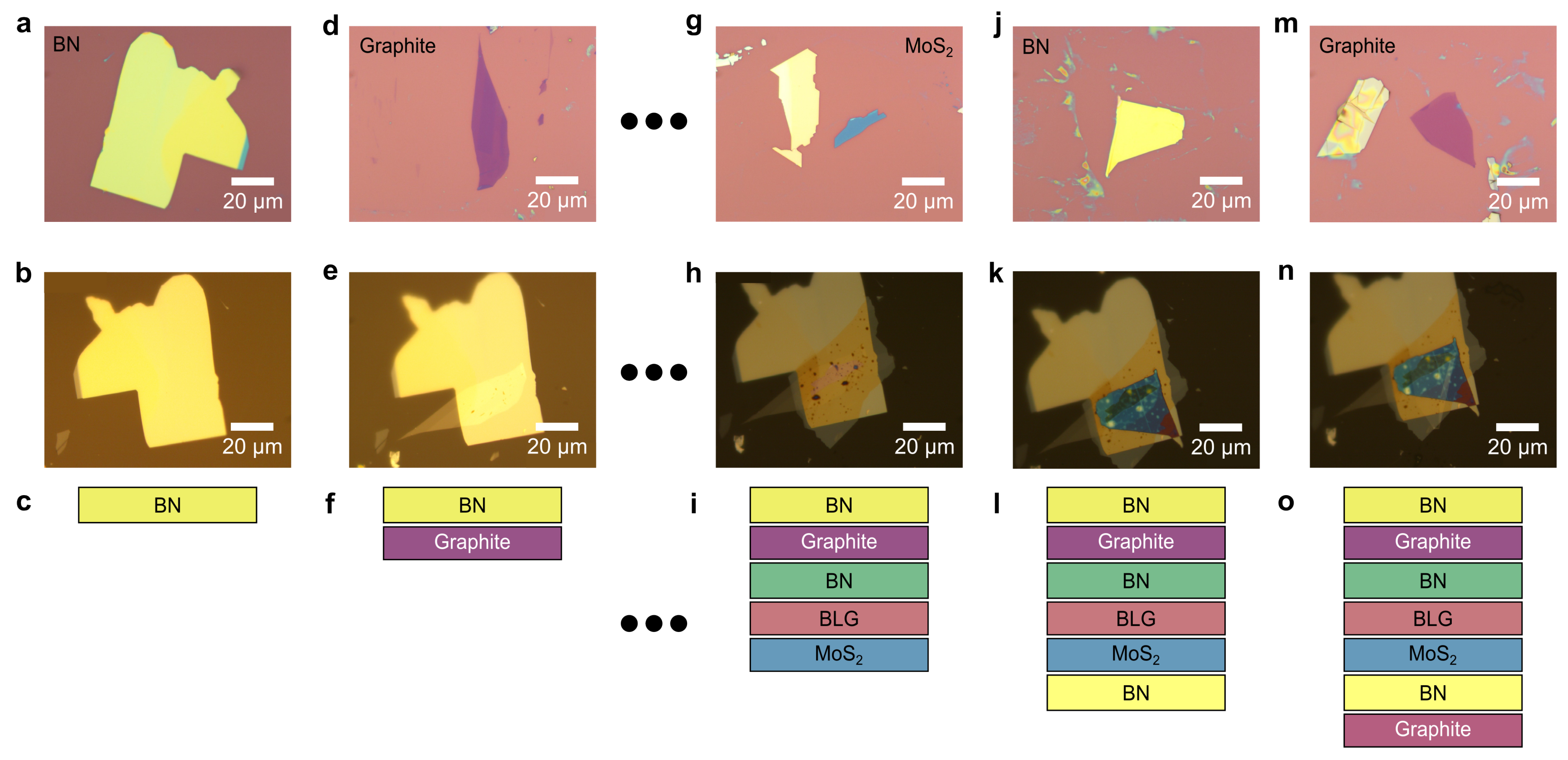
One advantage of nail polish as a pick up polymer is that multi-material stacks can be fabricated without noticeable fatigue of the film. This may be due to the exact chemical composition of our nail polish of choice or simply the increased thickness of the film from a single drop allowing for more heating/cooling cycles before fatigue. Several stacking sequences of a seven layer stack created using our technique are shown in
Figure 2. An optical image of the first BN flake after exfoliation and before pick up is shown in
Figure 2a. An optical image of the pick up slide after picking up the BN flake is shown in
Figure 2b and a model representing this layer is shown in
Figure 2c. Subsequent layers follow this pattern. Two pick up sequences in the middle have been omitted for clarity. While adsorbate bubbles appear with each new layer, no significant folds or cracks are present that would hinder final device creation.
While stacks such as these are possible with our polish of choice (Revlon Nail Enamel, New York, NY, USA), we have found that not all clear nail polishes are created equal when it comes to heterostructure assembly. Although they are similar in transparency and viscosity, there are subtle differences between pick up and transfer capabilities that are not obvious until experimentation. We performed pick up trials on multiple brands of clear polish: Revlon Nail Enamel, Clear 771, Sinful Colors Professional Clear Coat, L.A. COLORS Color Last Crystal Top Coat, and Sally Hansen Miracle Gel Top Coat, New York, NY, USA. Of the four, the Revlon polish has been the most versatile, allowing easy pick up and transfer of all 2D flakes that were attempted. Sinful Colors successfully picks up flakes and does not fatigue. However the compound is not as adhesive as Revlon, and thus requires multiple pick-up attempts for the same flake. Sally Hansen Miracle Gel successfully picks up flakes but does not solidify completely after heating. The makeup of a gel polish consists of methacrylate monomer and a photoinitiator which requires ultraviolet light to harden. Lastly, we found that all attempts of flake pick up with L.A. COLORS failed. The compound appears less adhesive than both Sinful Colors and Revlon. A more cost effective and perhaps long term improvement on these initial results would be the development of a recipe with pure nitrocellulose dissolved in a suitable solvent.
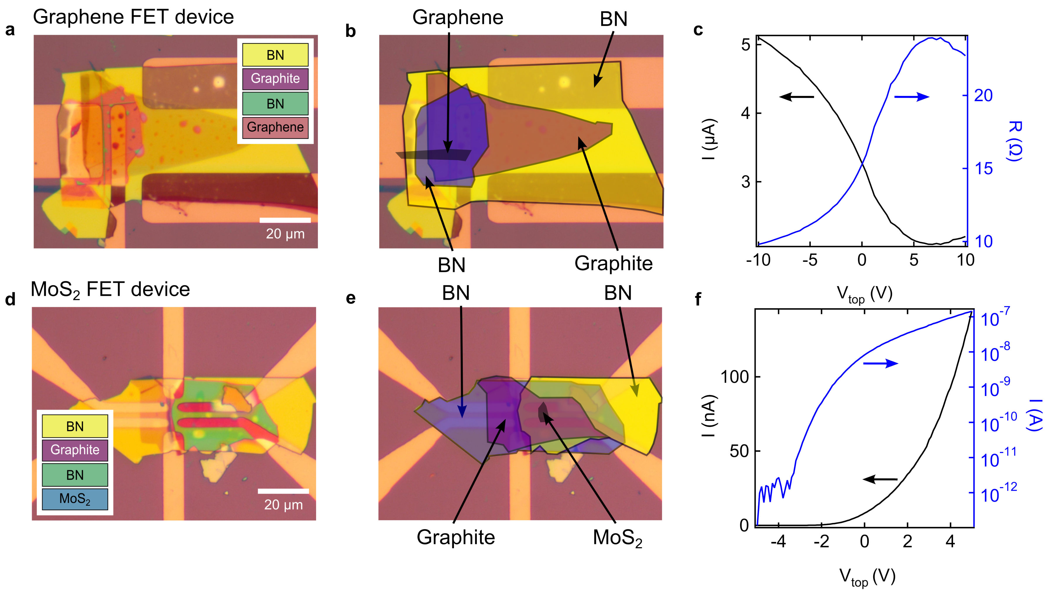
3. Field-Effect Transistors Fabricated Using Our Assembly Technique
To demonstrate the versatility of our technique, we present two field-effect transistors fabricated using nail polish and report their electrical characteristics. The optical images and electrical characteristics of the devices, one fabricated with graphene and one with MoS
2 are displayed in
Figure 3. Our assembly and transfer technique allows for quick fabrication, roughly 2.5 h for each stack, of such devices utilizing prepatterned electrodes. This amounts to a stacking rate of 1.6 flakes/h. This is equivalent to the time reported by Rebollo et al. for transfer of one flake [
18], less than an hour, and slightly faster than the automated stacking time, one flake per hour, reported by Masubuchi et al. [
21]. By precisely arranging the individual layers, they can be placed in contact with prepatterned electrodes on a Si/SiO
2 substrate to create an electrical device. The prepatterned electrodes are created using standard photolithography techniques. The gold electrodes are 20 nm thick and have a 5 nm thick sticking layer of chromium below them. It should be noted that while our technique works well for individually stacked devices, there may be better solutions for scalable transfer of 2D materials [
22,
23,
24].
A graphene device is shown in
Figure 3a–c and it consists of four flake layers. A large BN flake is used to pick up a graphite flake which is used as a top gate electrode. This electrode is isolated from the channel using another BN flake. The graphene is then picked up last. A schematic of the stack is shown in the inset of
Figure 3a. The stack is transferred to prepatterned gold electrodes on a Si/SiO
2 substrate. In
Figure 3b, each layer is shown using a transparent overlay of the same optical image in
Figure 3a. The narrow graphene flake forms a channel between the left-most two gold electrodes. The top gate graphite flake makes connection with the top-most gold electrode. The drain current (
I) as a function of top-gate voltage (
) at a bias of 50 mV is shown in
Figure 3c. The corresponding resistance (
R) is plotted on the right axis of the same plot. A resistance peak is apparent around
V corresponding to charge neutrality (or the Dirac point) in graphene. Charge neutrality is shifted significantly from
V, indicating residual doping, most likely due to surface water at the interface between the graphene flake and SiO
2 [
25,
26,
27,
28].
An MoS
2 FET is shown in
Figure 3d–f. The four layer stack is similar to the first graphene device but an MoS
2 flake is picked up instead of graphene. An optical image of the device is shown in
Figure 3d and a model of the stack is shown in the inset. In
Figure 3e, each layer is shown using a colored overlay. The MoS
2 flake forms a channel between the right-most two electrodes and the top-gate graphite flake makes contact with the left-most two electrodes. The drain current plotted as a function of top-gate voltage at a bias voltage of 500 mV is shown in
Figure 3f. The log current is plotted on the right axis. A clear n-type transistor action is recorded with an On/Off ratio of
.


 and
and 