
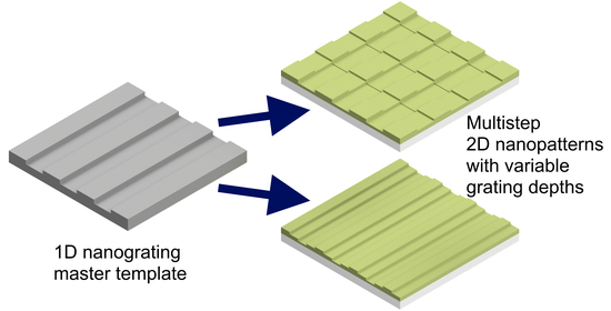
Two-Dimensional Nanograting Fabrication by Multistep Nanoimprint Lithography and Ion Beam Etching


Abstract
:
1. Introduction
2. Materials and Methods
3. Results
4. Discussion
Author Contributions
Funding
Data Availability Statement
Conflicts of Interest
References
- Tang, C.W.; VanSlyke, S.A. Organic electroluminescent diodes. Appl. Phys. Lett. 1987, 51, 913–915. [Google Scholar] [CrossRef]
- Reineke, S.; Lindner, F.; Schwartz, G.; Seidler, N.; Walzer, K.; Lüssem, B.; Leo, K. White organic light-emitting diodes with fluorescent tube efficiency. Nature 2009, 459, 234–238. [Google Scholar] [CrossRef]
- Shaheen, S.E.; Brabec, C.J.; Sariciftci, N.S.; Padinger, F.; Fromherz, T.; Hummelen, J.C. 2.5% efficient organic plastic solar cells. Appl. Phys. Lett. 2001, 78, 841–843. [Google Scholar] [CrossRef] [Green Version]
- Li, S.; Ye, L.; Zhao, W.; Yan, H.; Yang, B.; Liu, D.; Li, W.; Ade, H.; Hou, J. A Wide Band Gap Polymer with a Deep Highest Occupied Molecular Orbital Level Enables 14.2% Efficiency in Polymer Solar Cells. J. Am. Chem. Soc. 2018, 140, 7159–7167. [Google Scholar] [CrossRef] [PubMed]
- Meerheim, R.; Furno, M.; Hofmann, S.; Lüssem, B.; Leo, K. Quantification of energy loss mechanisms in organic light-emitting diodes. Appl. Phys. Lett. 2010, 97, 253305. [Google Scholar] [CrossRef]
- Furno, M.; Rosenow, T.C.; Gather, M.C.; Lüssem, B.; Leo, K. Analysis of the external and internal quantum efficiency of multi-emitter, white organic light emitting diodes. Appl. Phys. Lett. 2012, 101, 143304. [Google Scholar] [CrossRef]
- Mladenovski, S.; Neyts, K.; Pavicic, D.; Werner, A.; Rothe, C. Exceptionally efficient organic light emitting devices using high refractive index substrates. Opt. Express 2009, 17, 7562–7570. [Google Scholar] [CrossRef] [PubMed] [Green Version]
- Möller, S.; Forrest, S.R. Improved light out-coupling in organic light emitting diodes employing ordered microlens arrays. J. Appl. Phys. 2002, 91, 3324–3327. [Google Scholar] [CrossRef] [Green Version]
- Li, Y.; Kovačič, M.; Westphalen, J.; Oswald, S.; Ma, Z.; Hänisch, C.; Will, P.-A.; Jiang, L.; Junghaehnel, M.; Scholz, R.; et al. Tailor-made nanostructures bridging chaos and order for highly efficient white organic light-emitting diodes. Nat. Commun. 2019, 10, 2972. [Google Scholar] [CrossRef]
- Do, Y.R.; Kim, Y.-C.; Song, Y.-W.; Lee, Y.-H. Enhanced light extraction efficiency from organic light emitting diodes by insertion of a two-dimensional photonic crystal structure. J. Appl. Phys. 2004, 96, 7629–7636. [Google Scholar] [CrossRef] [Green Version]
- Jeon, S.; Kang, J.-W.; Park, H.-D.; Kim, J.-J.; Youn, J.R.; Shim, J.; Jeong, J.; Choi, D.-G.; Kim, K.-D.; Altun, A.O.; et al. Ultraviolet nanoimprinted polymer nanostructure for organic light emitting diode application. Appl. Phys. Lett. 2008, 92, 223307. [Google Scholar] [CrossRef]
- Ishihara, K.; Fujita, M.; Matsubara, I.; Asano, T.; Noda, S.; Ohata, H.; Hirasawa, A.; Nakada, H.; Shimoji, N. Organic light-emitting diodes with photonic crystals on glass substrate fabricated by nanoimprint lithography. Appl. Phys. Lett. 2007, 90, 111114. [Google Scholar] [CrossRef]
- Jiang, W.; Liu, H.; Yin, L.; Ding, Y. Fabrication of well-arrayed plasmonic mesoporous TiO2/Ag films for dye-sensitized solar cells by multiple-step nanoimprint lithography. J. Mater. Chem. A 2013, 1, 6433–6440. [Google Scholar] [CrossRef]
- Geyer, U.; Hauss, J.; Riedel, B.; Gleiss, S.; Lemmer, U.; Gerken, M. Large-scale patterning of indium tin oxide electrodes for guided mode extraction from organic light-emitting diodes. J. Appl. Phys. 2008, 104, 93111. [Google Scholar] [CrossRef]
- Riedel, B.; Hauss, J.; Geyer, U.; Guetlein, J.; Lemmer, U.; Gerken, M. Enhancing outcoupling efficiency of indium-tin-oxide-free organic light-emitting diodes via nanostructured high index layers. Appl. Phys. Lett. 2010, 96, 243302. [Google Scholar] [CrossRef]
- Choi, J.; Koh, T.-W.; Lee, S.; Yoo, S. Enhanced light extraction in organic light-emitting devices: Using conductive low-index layers and micropatterned indium tin oxide electrodes with optimal taper angle. Appl. Phys. Lett. 2012, 100, 233303. [Google Scholar] [CrossRef] [Green Version]
- Kluge, C.; Rädler, M.; Pradana, A.; Bremer, M.; Jakobs, P.-J.; Barié, N.; Guttmann, M.; Gerken, M. Extraction of guided modes from organic emission layers by compound binary gratings. Opt. Lett. 2012, 37, 2646–2648. [Google Scholar] [CrossRef]
- Fujita, M.; Ueno, T.; Ishihara, K.; Asano, T.; Noda, S.; Ohata, H.; Tsuji, T.; Nakada, H.; Shimoji, N. Reduction of operating voltage in organic light-emitting diode by corrugated photonic crystal structure. Appl. Phys. Lett. 2004, 85, 5769–5771. [Google Scholar] [CrossRef] [Green Version]
- Fujita, M.; Ishihara, K.; Ueno, T.; Asano, T.; Noda, S.; Ohata, H.; Tsuji, T.; Nakada, H.; Shimoji, N. Optical and Electrical Characteristics of Organic Light-Emitting Diodes with Two-Dimensional Photonic Crystals in Organic/Electrode Layers. Jpn. J. Appl. Phys. 2005, 44, 3669–3677. [Google Scholar] [CrossRef]
- Lüder, H.; Gerken, M. FDTD modelling of nanostructured OLEDs: Analysis of simulation parameters for accurate radiation patterns. Opt. Quantum Electron. 2019, 51, 139. [Google Scholar] [CrossRef] [Green Version]
- Schwab, T.; Fuchs, C.; Scholz, R.; Zakhidov, A.; Leo, K.; Gather, M.C. Coherent mode coupling in highly efficient top-emitting OLEDs on periodically corrugated substrates. Opt. Express 2014, 22, 7524–7537. [Google Scholar] [CrossRef] [PubMed] [Green Version]
- Zhang, S.; Turnbull, G.A.; Samuel, I.D.W. Highly Directional Emission and Beam Steering from Organic Light-Emitting Diodes with a Substrate Diffractive Optical Element. Adv. Opt. Mater. 2014, 2, 343–347. [Google Scholar] [CrossRef] [Green Version]
- Polywka, A.; Tückmantel, C.; Görrn, P. Light controlled assembly of silver nanoparticles. Sci. Rep. 2017, 7, 45144. [Google Scholar] [CrossRef] [PubMed] [Green Version]
- Iwahashi, T.; Yang, R.; Okabe, N.; Sakurai, J.; Lin, J.; Matsunaga, D. Nanoimprint-assisted fabrication of high haze metal mesh electrode for solar cells. Appl. Phys. Lett. 2014, 105, 223901. [Google Scholar] [CrossRef]
- Keum, C.; Murawski, C.; Archer, E.; Kwon, S.; Mischok, A.; Gather, M.C. A substrateless, flexible, and water-resistant organic light-emitting diode. Nat. Commun. 2020, 11, 1–9. [Google Scholar] [CrossRef] [PubMed]
- Yokota, T.; Zalar, P.; Kaltenbrunner, M.; Jinno, H.; Matsuhisa, N.; Kitanosako, H.; Tachibana, Y.; Yukita, W.; Koizumi, M.; Someya, T. Ultraflexible organic photonic skin. Sci. Adv. 2016, 2, e1501856. [Google Scholar] [CrossRef] [Green Version]
- Ryu, G.S.; You, J.; Kostianovskii, V.; Lee, E.B.; Kim, Y.; Park, C.; Noh, Y.Y. Flexible and Printed PPG Sensors for Estimation of Drowsiness. IEEE Trans. Electron Devices 2018, 65, 2997–3004. [Google Scholar] [CrossRef]
- Liu, Y.-F.; Feng, J.; Bi, Y.-G.; Yin, D.; Sun, H.-B. Recent Developments in Flexible Organic Light-Emitting Devices. Adv. Mater. Technol. 2019, 4, 1800371. [Google Scholar] [CrossRef] [Green Version]
- Wang, R.; Xu, L.-H.; Li, Y.-Q.; Zhou, L.; Li, C.; Ou, Q.-D.; Chen, J.-D.; Shen, S.; Tang, J.-X. Broadband Light Out-Coupling Enhancement of Flexible Organic Light-Emitting Diodes Using Biomimetic Quasirandom Nanostructures. Adv. Opt. Mater. 2015, 3, 203–210. [Google Scholar] [CrossRef]
- Pradana, A.; Kluge, C.; Gerken, M. Tailoring the refractive index of nanoimprint resist by blending with TiO_2 nanoparticles. Opt. Mater. Express 2014, 4, 329. [Google Scholar] [CrossRef]
- Pradana, A.; Gerken, M. Photonic crystal slabs in flexible organic light-emitting diodes. Photonics Res. 2015, 3, 32. [Google Scholar] [CrossRef]
- Peng, W.; Wu, H. Flexible and Stretchable Photonic Sensors Based on Modulation of Light Transmission. Adv. Opt. Mater. 2019, 7, 1900329. [Google Scholar] [CrossRef]
- Karrock, T.; Paulsen, M.; Gerken, M. Flexible photonic crystal membranes with nanoparticle high refractive index nanoparticle layers. Beilstein J. Nanotechnol. 2017, 8, 203–209. [Google Scholar] [CrossRef] [PubMed] [Green Version]
- Kudryashov, V.; Yuan, X.-C.; Cheong, W.-C.; Radhakrishnan, K. Grey scale structures formation in SU-8 with e-beam and UV. Microelectron. Eng. 2003, 67–68, 306–311. [Google Scholar] [CrossRef]
- Mohamed, K.; Alkaisi, M.M.; Blaikie, R.J. Fabrication of three dimensional structures for an UV curable nanoimprint lithography mold using variable dose control with critical-energy electron beam exposure. J. Vac. Sci. Technol. B Microelectron. Nanom. Struct. Process. Meas. Phenom. 2007, 25, 2357–2360. [Google Scholar] [CrossRef]
- Mattelin, M.-A.; Radosavljevic, A.; Missinne, J.; Cuypers, D.; Van Steenberge, G. Design and fabrication of blazed gratings for a waveguide-type head mounted display. Opt. Express 2020, 28, 11175–11190. [Google Scholar] [CrossRef] [PubMed]
- Piaszenski, G.; Barth, U.; Rudzinski, A.; Rampe, A.; Fuchs, A.; Bender, M.; Plachetka, U. 3D structures for UV-NIL template fabrication with grayscale e-beam lithography. Microelectron. Eng. 2007, 84, 945–948. [Google Scholar] [CrossRef]
- Hasan, R.M.M.; Luo, X. Promising Lithography Techniques for Next-Generation Logic Devices. Nanomanuf. Metrol. 2018, 1, 67–81. [Google Scholar] [CrossRef] [Green Version]
- Huang, W.; Yu, X.; Liu, Y.; Qiao, W.; Chen, L. A review of the scalable nano-manufacturing technology for flexible devices. Front. Mech. Eng. 2017, 12, 99–109. [Google Scholar] [CrossRef]
- Sreenivasan, S.V. Nanoimprint lithography steppers for volume fabrication of leading-edge semiconductor integrated circuits. Microsyst. Nanoeng. 2017, 3, 1–19. [Google Scholar] [CrossRef] [PubMed] [Green Version]
- Traub, M.C.; Longsine, W.; Truskett, V.N. Advances in Nanoimprint Lithography. Annu. Rev. Chem. Biomol. Eng. 2016, 7, 583–604. [Google Scholar] [CrossRef] [PubMed]
- Shao, J.Y.; Chen, X.L.; Li, X.M.; Tian, H.M.; Wang, C.H.; Lu, B.H. Nanoimprint lithography for the manufacturing of flexible electronics. Sci. China Technol. Sci. 2019, 62, 175–198. [Google Scholar] [CrossRef]
- Hemmati, H.; Magnusson, R. Development of tuned refractive-index nanocomposites to fabricate nanoimprinted optical devices. Opt. Mater. Express 2018, 8, 175–183. [Google Scholar] [CrossRef]
- Hansen, M.; Ziegler, M.; Kohlstedt, H.; Pradana, A.; Raedler, M.; Gerken, M. UV capillary force lithography for multiscale structures. J. Vac. Sci. Technol. B 2012, 30, 31601. [Google Scholar] [CrossRef]
- Schift, H. Nanoimprint lithography: 2D or not 2D? A review. Appl. Phys. A 2015, 121, 415–435. [Google Scholar] [CrossRef]
- Harrer, S.; Yang, J.K.W.; Berggren, K.K.; Ilievski, F.; Ross, C.A. Pattern Generation by Using Multi-Step Room-Temperature Nanoimprint Lithography. In Proceedings of the 2006 Sixth IEEE Conference on Nanotechnology, Cincinnati, OH, USA, 17–20 July 2006; Volume 2, pp. 576–579. [Google Scholar]
- Jahns, S.; Bräu, M.; Meyer, B.-O.; Karrock, T.; Gutekunst, S.B.; Blohm, L.; Selhuber-Unkel, C.; Buhmann, R.; Nazirizadeh, Y.; Gerken, M. Handheld imaging photonic crystal biosensor for multiplexed, label-free protein detection. Biomed. Opt. Express 2015, 6, 3724–3736. [Google Scholar] [CrossRef] [Green Version]
- Glinsner, T.; Lindner, P.; Mühlberger, M.; Bergmair, I.; Schöftner, R.; Hingerl, K.; Schmid, H.; Kley, E.-B. Fabrication of 3D-photonic crystals via UV-nanoimprint lithography. J. Vac. Sci. Technol. B Microelectron. Nanom. Struct. Process. Meas. Phenom. 2007, 25, 2337–2340. [Google Scholar] [CrossRef]
- Shibata, T.; Ikeda, H.; Nishiyama, H.; Tawa, K.; Nishii, J. Optimization of Metal Quality for Grating Coupled Surface Plasmon Resonance. Phys. Procedia 2013, 48, 179–183. [Google Scholar] [CrossRef] [Green Version]


Publisher’s Note: MDPI stays neutral with regard to jurisdictional claims in published maps and institutional affiliations. |
© 2021 by the authors. Licensee MDPI, Basel, Switzerland. This article is an open access article distributed under the terms and conditions of the Creative Commons Attribution (CC BY) license (https://creativecommons.org/licenses/by/4.0/).
Share and Cite
Buhl, J.; Yoo, D.; Köpke, M.; Gerken, M. Two-Dimensional Nanograting Fabrication by Multistep Nanoimprint Lithography and Ion Beam Etching. Nanomanufacturing 2021, 1, 39-48. https://doi.org/10.3390/nanomanufacturing1010004
Buhl J, Yoo D, Köpke M, Gerken M. Two-Dimensional Nanograting Fabrication by Multistep Nanoimprint Lithography and Ion Beam Etching. Nanomanufacturing. 2021; 1(1):39-48. https://doi.org/10.3390/nanomanufacturing1010004
Chicago/Turabian StyleBuhl, Janek, Danbi Yoo, Markus Köpke, and Martina Gerken. 2021. "Two-Dimensional Nanograting Fabrication by Multistep Nanoimprint Lithography and Ion Beam Etching" Nanomanufacturing 1, no. 1: 39-48. https://doi.org/10.3390/nanomanufacturing1010004
APA StyleBuhl, J., Yoo, D., Köpke, M., & Gerken, M. (2021). Two-Dimensional Nanograting Fabrication by Multistep Nanoimprint Lithography and Ion Beam Etching. Nanomanufacturing, 1(1), 39-48. https://doi.org/10.3390/nanomanufacturing1010004