
The Effect of Thickness and Surface Recombination Velocities on the Performance of Silicon Solar Cell


Abstract
1. Introduction
2. Device Structure
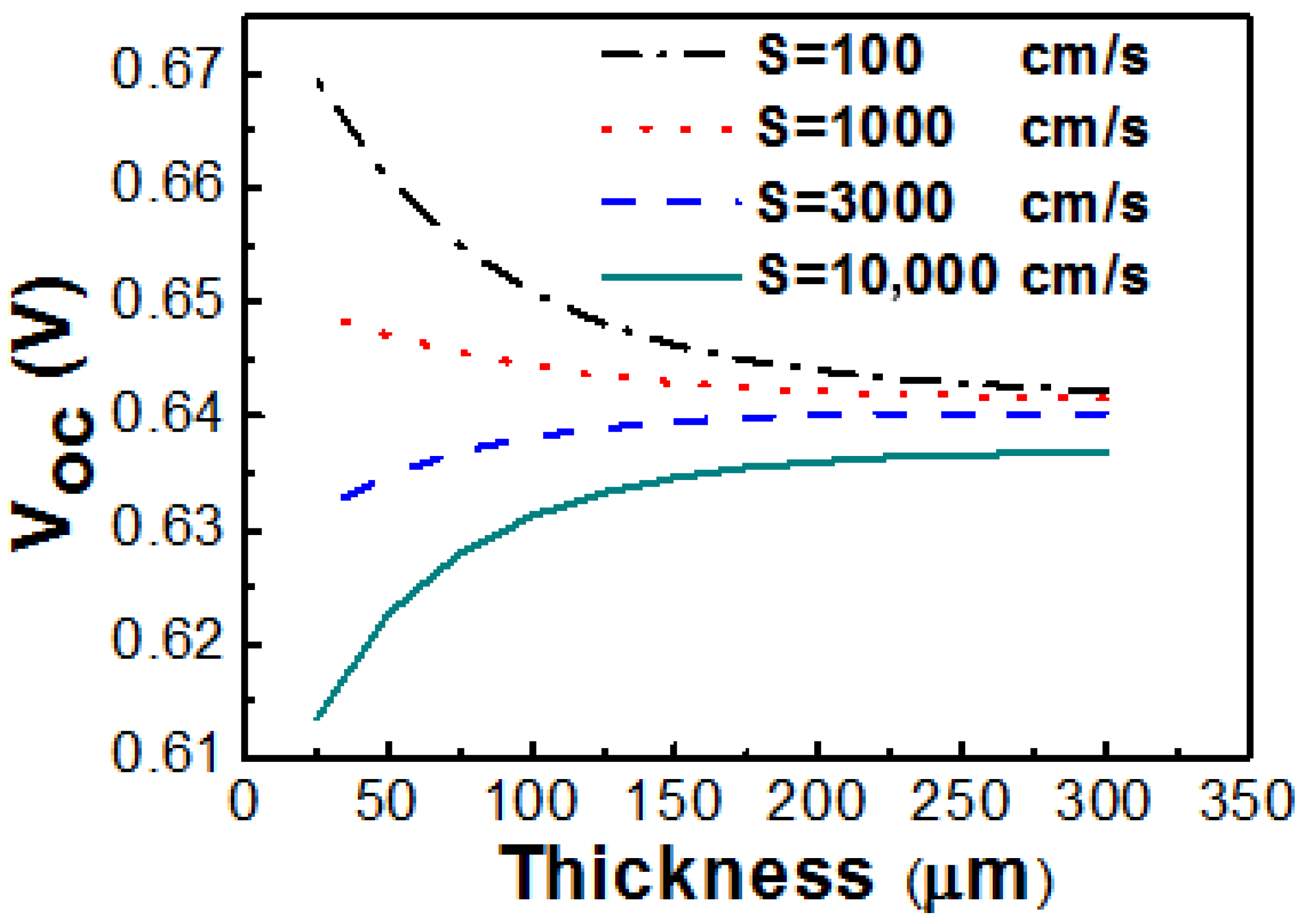
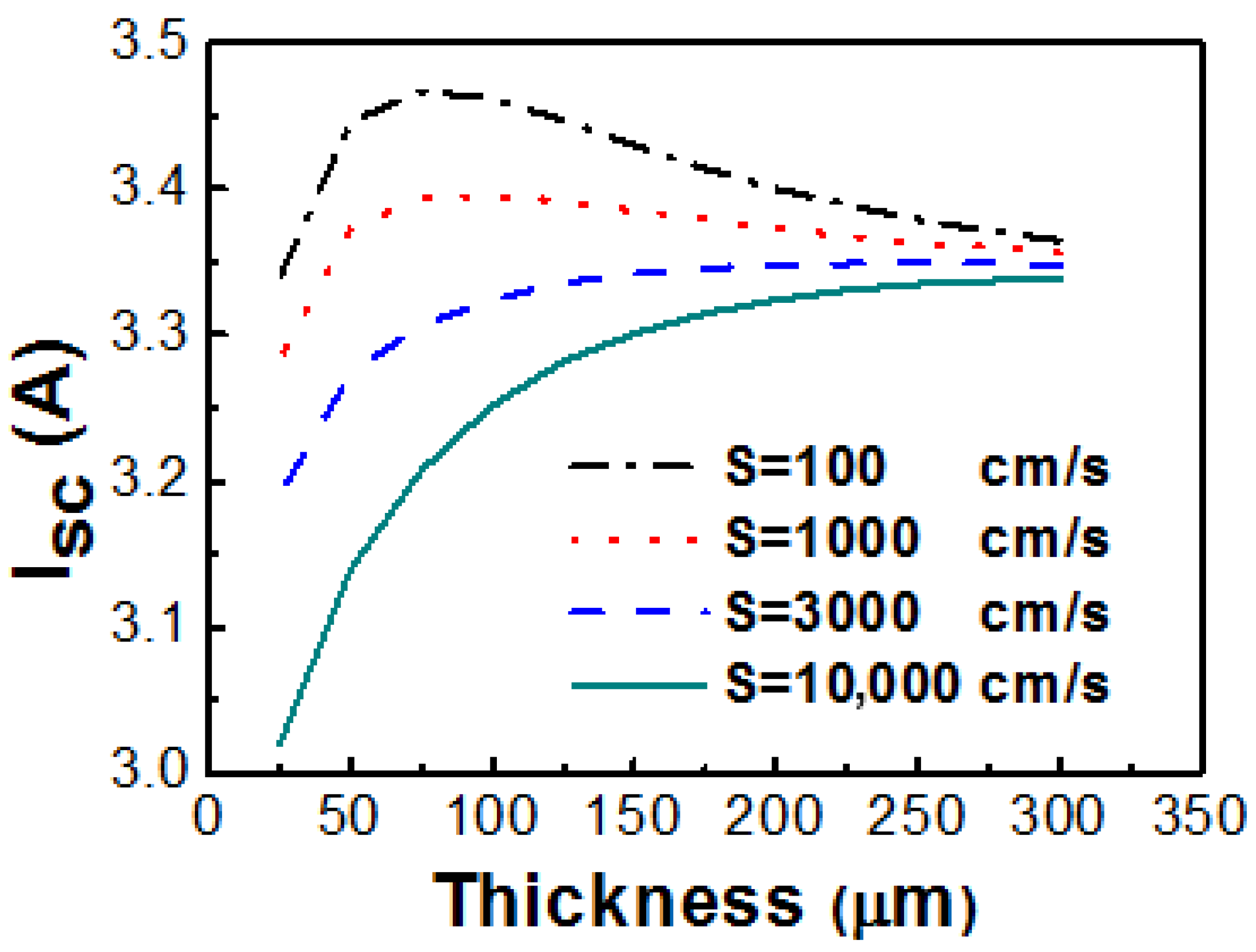
3. Results
4. Conclusions
Author Contributions
Funding
Data Availability Statement
Conflicts of Interest
References
- Kumar, P.M.; Kamruzzaman, M.M.; Alfurhood, B.S.; Hossain, B.; Nagarajan, H.; Sitaraman, S.R. Balanced Performance Merit on Wind and Solar Energy Contact with Clean Environment Enrichment. IEEE J. Electron Devices Soc. 2024, 12, 808–823. [Google Scholar] [CrossRef]
- Sekar, S.; Thamotharan, K.; Manickam, S.; Murugesan, B.; Kakimoto, K.; Perumalsamy, R. A Critical Review of The Process and Challenges of Silicon Crystal Growth for Photovoltaic Applications. Cryst. Res. Technol. 2024, 59, 2300131. [Google Scholar] [CrossRef]
- Xu, C.; Isabella, O.; Vogt, M.R. Future material demand for global silicon-based PV modules under net-zero emissions target until 2050. Resour. Conserv. Recycl. 2024, 210, 107824. [Google Scholar] [CrossRef]
- Zeng, L.; Bermel, P.; Yi, Y.; Alamariu, B.A.; Broderick, K.A.; Liu, J.; Hong, C.; Duan, X.; Joannopoulos, J.; Kimerling, L.C. Demonstration of enhanced absorption in thin film Si solar cells with textured photonic crystal back reflector. Appl. Phys. Lett. 2008, 93, 221105. [Google Scholar] [CrossRef]
- Tool, C.J.J.; Burgers, A.R.; Manshanden, P.; Weeber, A.W.; van Straaten, B.H.M. Influence of wafer thickness on the performance of multicrystalline Si solar cells: An experimental study. Prog. Photovolt Res. Appl. 2002, 10, 279–291. [Google Scholar] [CrossRef]
- Wolf, M.; Ralph, E.L. Effect of thickness on short-circuit current of silicon solar cells. IEEE Trans. Electron Dev. 1965, 12, 470–474. [Google Scholar] [CrossRef]
- Sah, C.-T.; Yamakawa, K.A.; Lutwack, R. Effect of thickness on silicon solar cell efficiency. IEEE Trans. Electron Dev. 1982, 29, 903–908. [Google Scholar] [CrossRef]
- Warta, W.; Glunz, S.W.; Dicker, J.; Knobloch, J. Highly efficient 115-μm-thick solar cells on industrial Czochralski silicon. Prog. Photovolt Res. Appl. 2000, 8, 465–471. [Google Scholar] [CrossRef]
- Clugston, D.A.; Basore, P.A. PClD Version 5: 32-Bit Solar Cell Modeling on Personal Computers. In Proceedings of the 26th IEEE Photovoltaic Specialists Conference, Anaheim, CA, USA, 29 September–3 October 1997; p. 207. [Google Scholar]
- Thirunavukkarasu, G.S.; Seyedmahmoudian, M.; Chandran, J.; Stojcevski, A.; Subramanian, M.; Marnadu, R.; Alfaify, S.; Shkir, M. Optimization of Mono-Crystalline Silicon Solar Cell Devices Using PC1D Simulation. Energies 2021, 14, 4986. [Google Scholar] [CrossRef]
- Roshi, B.; Singh, B.; Gupta, V. Modelling and simulation of silicon solar cells using PC1D. Mater. Today Proc. 2022, 54, 810–813. [Google Scholar] [CrossRef]
- Kim, J.; Lee, S.; Chowdhury, S.; Yi, J. A Brief Review of Passivation Materials and Process for High Efficiency PERC Solar Cell. Trans. Electr. Electron. Mater. 2021, 23, 1–5. [Google Scholar] [CrossRef]
- Hallam, B.; Kim, M.; Zhang, Y.; Wang, L.; Lennon, A.; Verlinden, P.; Altermat, P.P.; Dias, P.R. The silver learning curve for photovoltaics and projected silver demand for net-zero emissions by 2050. Prog. Photovolt Res. Appl. 2022, 31, 598–606. [Google Scholar] [CrossRef]
- Zhou, Y.; Zhao, D.; Yu, X.; Li, M.; Zhao, Z.; Chen, C.; Lin, Z.; Wang, L.; Chen, X.; Li, X.; et al. Ultra-thin silicon oxide tunnel layer passivated contacts for screen-printed n-type industry solar cells. Sol. Energy Mater. Sol. Cells 2024, 266, 112657. [Google Scholar] [CrossRef]
- Saeed, R.; Tahir, S.; Ali, A.; Albalawi, H.; Ashfaq, A. AFORS-HET-based numerical exploration of tunnel oxide passivated contact solar cells incorporating nand p-type silicon substrates. RSC Adv. 2024, 14, 22253–22265. [Google Scholar] [CrossRef] [PubMed]
- Green, M.A. Solar Cells: Operating Principles, Technology and System Applications; University of New South Wales: Kensington, Australia, 1992; Section 4.9. [Google Scholar]
- Honsberg, C.B.; Bowden, S.G. Photovoltaics Education Website. 2019. Available online: https://www.pveducation.org/pvcdrom/pn-junctions/generation-rate (accessed on 30 June 2025).
- Angermann, H.; Rappich, J.; Korte, L.; Sieber, I.; Conrad, E.; Schmidt, M.; Hubener, K.; Polte, J.; Hauschild, J. Wet-chemical passivation of atomically flat and structured silicon substrates for solar cell application. Appl. Surf. Sci. 2008, 254, 3615–3625. [Google Scholar] [CrossRef]
- Pain, S.L.; Khorani, E.; Niewelt, T.; Wratten, A.; Paez Fajardo, G.J.; Winfield, B.P.; Bonilla, R.S.; Walker, M.; Piper, L.F.J.; Grant, N.E.; et al. Electronic Characteristics of Ultra-Thin Passivation Layers for Silicon Photovoltaics. Adv. Mater. Interfaces 2022, 9, 2201339. [Google Scholar] [CrossRef]
- Glunz, S.W.; Steinhauser, B.; Polzin, J.I.; Luderer, C.; Grübel, B.; Niewelt, T.; Okasha, A.M.O.M.; Bories, M.; Nagel, H.; Krieg, K.; et al. Silicon-based passivating contacts: The TOPCon route. Prog. Photovolt Res. Appl. 2023, 31, 341–359. [Google Scholar] [CrossRef]
- Veirman, J.; Varache, R.; Albaric, M.; Danel, A.; Guo, B.; Fu, N.; Wang, Y.C. Silicon wafers for industrial n-type SHJ solar cells: Bulk quality requirements, large-scale availability and guidelines for future developments. Sol. Energy Mater. Sol. Cells 2021, 228, 111128. [Google Scholar] [CrossRef]


| Parameters | Value |
|---|---|
| Cell area | 100 cm2 |
| Front surface texture depth | 3 mm |
| Exterior front reflection | 10% |
| Base contact | 1.5 × 10⁻³ Ω |
| Dielectric constant | 11.9 |
| Band gap | 1.12 |
| Intrinsic concentration | 1 × 1010 cm−3 |
| Bulk recombination | tn = tp = 7.2 ms |
| Temperature | 25 °C |
| Light intensity | 0.1 Wcm−2 |
| Light spectrum | AM 1.5G |
Disclaimer/Publisher’s Note: The statements, opinions and data contained in all publications are solely those of the individual author(s) and contributor(s) and not of MDPI and/or the editor(s). MDPI and/or the editor(s) disclaim responsibility for any injury to people or property resulting from any ideas, methods, instructions or products referred to in the content. |
© 2025 by the authors. Licensee MDPI, Basel, Switzerland. This article is an open access article distributed under the terms and conditions of the Creative Commons Attribution (CC BY) license (https://creativecommons.org/licenses/by/4.0/).
Share and Cite
Lin, C.-H.; Huang, L.-C. The Effect of Thickness and Surface Recombination Velocities on the Performance of Silicon Solar Cell. Solids 2025, 6, 33. https://doi.org/10.3390/solids6030033
Lin C-H, Huang L-C. The Effect of Thickness and Surface Recombination Velocities on the Performance of Silicon Solar Cell. Solids. 2025; 6(3):33. https://doi.org/10.3390/solids6030033
Chicago/Turabian StyleLin, Chu-Hsuan, and Li-Cyuan Huang. 2025. "The Effect of Thickness and Surface Recombination Velocities on the Performance of Silicon Solar Cell" Solids 6, no. 3: 33. https://doi.org/10.3390/solids6030033
APA StyleLin, C.-H., & Huang, L.-C. (2025). The Effect of Thickness and Surface Recombination Velocities on the Performance of Silicon Solar Cell. Solids, 6(3), 33. https://doi.org/10.3390/solids6030033