Article

Enhanced Assessment of Transition Metal Copper Sulfides via Classification of Density of States Spectra

by
Md Tohidul Islam
1,
Catalina Victoria Ruiz
2,
Claudia Loyola
2,
Joaquin Peralta
2 and
Scott R. Broderick
1,*
1
Department of Materials Design and Innovation, University at Buffalo, 12 Capen Hall, Buffalo, NY 14260, USA
2
Departamento de Física y Astronomía, Facultad de Ciencias Exactas, Universidad Andrés Bello, Sazié 2212, piso 7, Santiago 8370136, Chile
*
Author to whom correspondence should be addressed.
Solids 2025, 6(3), 32; https://doi.org/10.3390/solids6030032
Submission received: 16 April 2025 / Revised: 15 June 2025 / Accepted: 18 June 2025 / Published: 25 June 2025

Abstract

Understanding how crystal structure influences electronic properties is crucial for discovering new functional materials. In this study, we utilized Kernel Principal Component Analysis (KPCA) to classify and analyze the Density of States (DOS) of transition metal sulfide (TMS) compounds, particularly copper-based sulfides. By mapping high-dimensional DOS data into a lower-dimensional space, we identify clusters corresponding to different crystal systems and detect outliers with significant deviations from their expected groups. These outliers exhibit unusual electronic configurations, suggesting potential applications in semiconductors, thermoelectric devices, and optoelectronic devices. Projected Density of States (PDOS) analysis further reveals how orbital hybridization governs the electronic structure of these materials, highlighting key differences between structurally similar compounds. Additionally, we analyze phase stability through inter-cluster distance measurements, identifying potential phase transformations between closely related structures. The implications for this work in terms of modifying chemistries and generalized DOS predictions are discussed.

1. Introduction

The electronic properties of materials play a fundamental role in their applications across various technological domains, including semiconductors [1,2], superconductors [3,4], optoelectronics [5], and energy storage [6,7]. The Density of States (DOS), which describes the number of electronic states available at each energy level, is a key descriptor of a material’s electronic behavior [8]. The analysis of DOS can provide critical information about bandgaps, conductivity, hybridization effects, and orbital contributions, which determine whether a material behaves as a metal, semiconductor, or insulator [9,10]. However, due to the high-dimensional nature of DOS data, extracting meaningful patterns and correlations across large datasets remains a challenge [11]. In particular, we focus on copper-containing sulfides (TM-Cu-S) as a case study due to their rich phase behavior and technological relevance.
High-throughput computational materials databases, such as the Materials Project, have enabled researchers to access and analyze extensive DOS datasets [12,13,14]. With the growing volume of electronic structure data, machine learning and dimensionality reduction techniques provide powerful tools to map high-dimensional electronic information into lower-dimensional representations. Among these techniques, Kernel Principal Component Analysis (KPCA) has emerged as a robust method for capturing nonlinear relationships in complex datasets, allowing materials with similar DOS characteristics to be grouped into clusters [15].
Traditionally, materials with the same crystal system are expected to exhibit similar electronic structures, yet deviations often arise due to differences in composition, bonding interactions, and hybridization effects. Identifying such outliers, (that is, materials that significantly deviate from their expected electronic behavior), provides valuable insight into unconventional electronic properties, potential phase transitions, and novel material functionalities. These deviations may indicate materials with unique transport properties, topological states, or correlated electron effects, which are of particular interest in quantum materials, thermoelectrics, and catalysis. Orbital hybridization plays a crucial role in defining the band structure, charge transport, and bonding characteristics of a material [16]. Strong d-orbital contributions, for instance, can lead to metallic behavior, magnetism, or Jahn–Teller distortions, while p-orbital hybridization is often associated with semiconducting and optical properties [17].
In this study, we explore how materials with different crystal systems group based on their DOS characteristics in a reduced-dimensional space. We identify materials that deviate significantly from their clusters, indicating unusual electronic structures. Further, we use PDOS analysis to investigate hybridization effects. Finally, we explore the role of chemistry and stoichiometry in shaping electronic configurations.

2. Methodology

2.1. Dataset and Preprocessing

The DOS data used in this study were obtained from the Materials Project database via the Materials API. The dataset consists of PDOS values for various materials, encompassing diverse crystal structures and electronic configurations. We selected 26 representative ternary Cu–S compounds containing transition metals (Ti, V, Cr, Fe, Co, Ni, Mo, W, etc.), encompassing the major structure types found in this chemical family. This focused dataset purposefully excludes ternaries with only main-group cations (e.g., Cu–In–S or Cu–Sn–S), which are numerous in databases but fall outside our scope of transition metal copper sulfides. Notably, some crystal systems are represented by only 1–2 compounds (e.g., only one hexagonal phase is known in this category), which limits intraclass statistical analysis. We include these for completeness while acknowledging the reduced support for those classes. Our dataset of 26 compounds encompasses seven crystal systems: triclinic (4 compounds), monoclinic (8), orthorhombic (6), tetragonal (2), cubic (4), trigonal (1), and hexagonal (1).
The energy axis was adjusted to set the Fermi level (EF) at zero, ensuring a standardized reference across all materials. To facilitate clustering and dimensionality reduction, the DOS curves were interpolated onto a common energy grid spanning −40 eV to +20 eV with a step size of 0.1 eV. The data was subsequently mean-centered to remove systematic offsets, followed by Min-Max normalization to scale features between 0 and 1 for consistent numerical stability. A total of 26 copper-containing ternary sulfides were analyzed in this study, encompassing seven distinct crystal systems: cubic, trigonal, monoclinic, orthorhombic, triclinic, and hexagonal. The crystal system describes the highest-level symmetry class of the Bravais lattice, whereas a structure type (e.g., chalcopyrite, spinel, sulvanite) is defined by the full space group. The latter provides a far more detailed description but would fragment our 26-compound dataset into many singletons, eliminating any statistical power. Grouping at the crystal-system level retains a minimum of two members in five of the seven classes and is still physically meaningful. Our analysis should thus be viewed as a coarse-grained screening step that captures symmetry-driven trends. Structure-type specific subtleties can then be explored in follow-up studies.
Nonlinear Feature Extraction via KPCA [18] has been used to analyze variations in DOS patterns and identify anomalous materials. Unlike linear PCA, KPCA projects the high-dimensional DOS features into a nonlinear feature space using a Radial Basis Function (RBF) kernel:
k x i , x j = exp γ | x i x j | 2
where k is the kernel matrix, and x i and x j represent the DOS vectors. The gamma parameter, which defines the kernel width and thus the sensitivity of the projection to feature space distances, was set to γ = 0.1 for optimal separation of material clusters in the transformed space. We systematically tuned the RBF kernel width parameter γ by performing a grid search from 0.01 to 1.0 in increments of 0.001. For each γ, we computed the Kernel PCA and evaluated the clustering quality using the average silhouette score (a higher silhouette score generally indicates that the clusters are more cohesive and well-separated), using the known crystal system labels. The silhouette score peaked at γ ≈ 0.071 (Supplementary Figure S1). We retained γ = 0.1 for the main analyses to maintain consistency with our earlier results, noting that both values fall within the same local maximum region of silhouette scores and produce similar clustering quality. This approach captures complex variations in the DOS profiles, making it particularly useful for distinguishing materials with subtle electronic structure differences [19]. The transformed data was then reduced to three principal components (PC1, PC2, PC3) for clustering and visualization. While PCA has previously been applied to DOS data to uncover patterns and trends [8], its linear nature limits its ability to capture more complex, nonlinear relationships among different materials. Therefore, we employed KPCA to enable the identification of nonlinear clustering structures that may not be accessible using linear dimensionality reduction techniques. KPCA offers key advantages for analyzing DOS spectra. Compared to supervised classification methods, KPCA does not require labeled training data. It captures nonlinear patterns in high-dimensional data that simpler methods might miss and does so without requiring labeled data. Unlike stochastic techniques like t-SNE or UMAP, KPCA provides deterministic components that can be quantitatively interpreted, linking features to energy ranges or orbitals.

2.2. Quantifying Structural Relationships Through Cluster Centroids and Distances

For each crystal system, we computed the centroid (mean position) in the 3D KPCA space:
Centroid = 1 N i = 1 N P C 1 i , P C 2 i , P C 3 i
where N is the number of materials in a given crystal system.
The Euclidean distance between each pair of centroids was calculated:
d A , B = P C 1 A P C 1 B 2 + P C 2 A P C 2 B 2 + P C 3 A P C 3 B 2
where A and B represent two different crystal systems.

2.3. The Convex Hull Analysis for Structural Classification and Outlier Identification

Clustering was performed using Convex Hull analysis [20], which encloses the data points corresponding to different crystal systems in the reduced KPCA space. The convex hull for each cluster is defined as follows:
Conv S = i λ i x i λ i 0 ,   i λ i = 1
where x i represents the materials in a given crystal system. Materials falling outside the convex hulls were flagged as potential outliers. Additionally, Euclidean distance analysis was conducted to quantify the deviation of each material from its respective cluster centroid:
d i j = | | C i C j | |
where C i and C j denote the centroids of different crystal systems. Materials exhibiting significantly large distances were identified as electronic anomalies. The convex hull provides a clear geometric enclosure around data points, helping to highlight extreme outliers that lie outside the general distribution. However, a key limitation is that it requires at least four non-coplanar points in three-dimensional space, making it ineffective for small datasets or cases where points are sparsely distributed.

2.4. Deviations in Electronic Structure

To investigate the unique electronic features of the outliers, we performed a detailed comparison of their projected density of states (PDOS) against those of the reference structures. Specifically, we examined how the s-, p-, and d-orbitals contribute to the total DOS and how these contributions may shift or reshape in the outlier systems. By analyzing orbital-projected DOS, we can assess the extent of orbital hybridization and gain insight into the nature of bonding and electron distribution within each material.
To define the partial density of states for an orbital O , we use the following:
D O E = i O ψ i E 2
where ψ i E are electronic wavefunctions at energy E . This expression quantifies the likelihood that a given orbital O contributes to the electron states near energy E . Notably, deviations in the shape, intensity, or position of the partial DOS peaks among the outliers can reveal altered bonding interactions or electronic configurations. These insights not only highlight the distinct electronic behavior of the outliers but also help clarify how changes in orbital character might influence their conduction, magnetic, or catalytic properties.

3. Results and Discussion

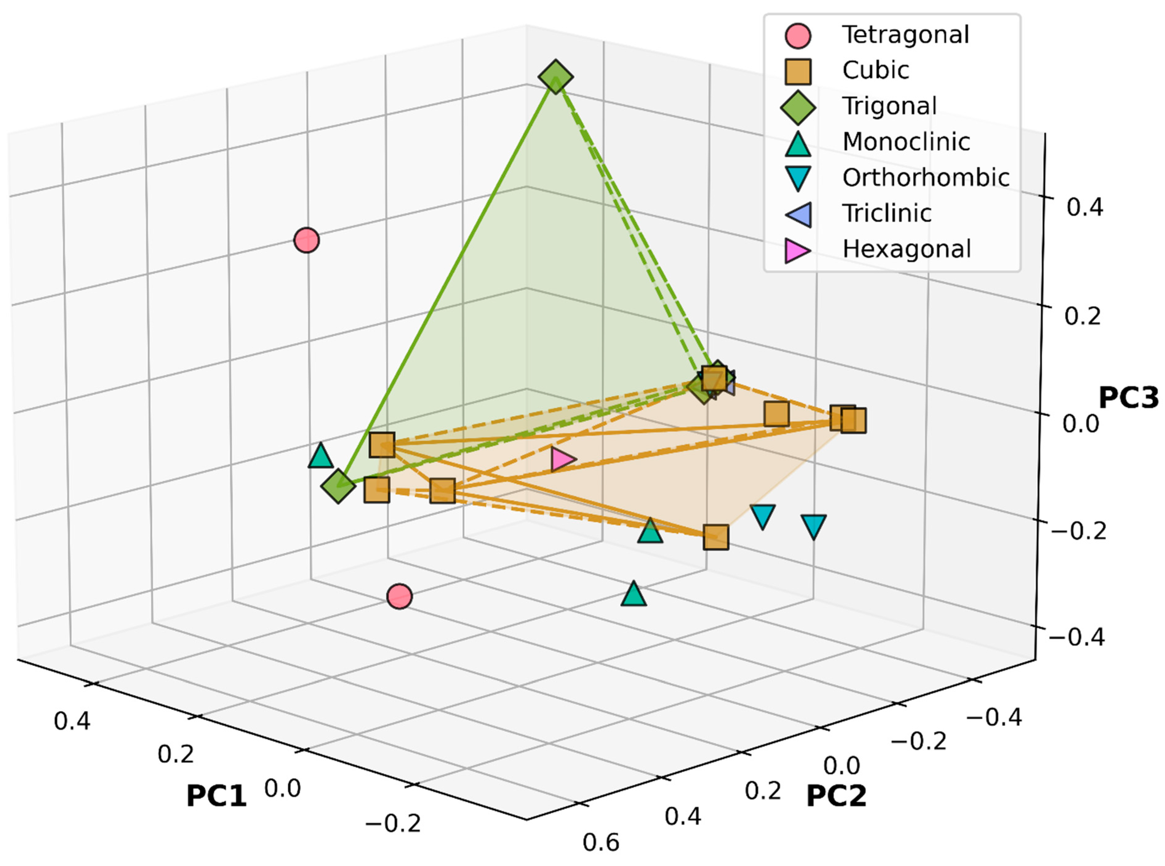
3.1. Crystal System Classification in Reduced-Dimensional KPCA Space

The electronic properties of materials are shaped not just by their chemical composition but also by their crystal structure and stoichiometry [21,22,23]. Figure 1a captures this relationship by clustering materials based on their DOS data using KPCA. The clear separation of different crystal systems suggests that structure plays a key role in determining electronic behavior. At the same time, some materials deviate significantly from their expected clusters. Separation of the clusters and some compositions suggest unique electronic features that might not be obvious from their chemistry alone. To gain a clearer picture, we included three additional projections—PC1–PC2, PC1–PC3, and PC2–PC3 (Figure 1b–d). Most materials cluster according to their crystal system. Symmetry also influences electronic structure. However, some materials, like Ti2CuS4, behave differently depending on their crystal phase, showing that even the same chemistry can lead to vastly different electronic configurations. Similarly, CrCuS2 and other materials in the trigonal and tetragonal groups stray from their expected clusters. Simply looking at DOS spectra would not allow us to pinpoint these outliers as effectively.
Since the electronic structure of a material exists in a high-dimensional space, directly analyzing it can be overwhelming. By reducing dimensionality and applying clustering techniques, we can uncover patterns and relationships that would otherwise be difficult to see, offering valuable insights into the connection between structure and electronic behavior. Figure 2 showcases the group based on their crystal structures when projected into a lower-dimensional space. The convex hulls enclose points belonging to the same crystal system. Tetragonal and hexagonal structures are more isolated. Cubic and Trigonal are well-clustered, and there is a shared region, meaning there can be polymorphism, and materials in these categories can exist in multiple phases. Electronic structures are closely linked to crystallographic arrangements, as materials sharing the same symmetry tend to cluster together. However, what stands out are the points that deviate significantly from these clusters—potential outliers that may indicate materials with electronic properties distinct from their expected group. These deviations suggest that even within the same stoichiometric framework, variations in chemistry (such as different transition metals in the B site) can influence the electronic structure enough to shift a material’s position in this reduced space. Having visualized how materials cluster by crystal system, we next focus on the materials that deviate from these clusters.
Outliers could exhibit novel electronic properties useful for semiconductors, catalysts, or superconductors. If these materials have tunable electronic properties, they could be optimized for targeted applications.
Detecting materials with unconventional electronic configurations is one of the key objectives to explore how materials with different crystal systems cluster based on their electronic structures. While materials within the same crystal system are expected to exhibit similar electronic characteristics, certain compositions may deviate significantly from their group. These deviations could indicate unusual electronic configurations, driven by differences in atomic coordination, bonding environment, or hybridization effects. These outliers represent compositions whose electronic structures differ notably from their expected crystal family, suggesting potential anomalies in their bonding interactions or orbital contributions. By detecting these deviations, we can identify materials that may exhibit unconventional electronic behavior, such as enhanced conductivity, bandgap modifications, or changes in hybridization patterns. In Figure 3, outliers are highlighted as red markers. The identified outliers—Ti(CuS)4, CrCuS2, VCu3S4, and Nb2CuS4—are positioned significantly outside their respective convex hulls. This suggests that their electronic structures do not conform to the typical trends observed for their assigned crystal systems, indicating structural variations, even within the same stoichiometry, can lead to substantial changes in the electronic properties of a material. Further investigation through PDOS analysis will help uncover the nature of these deviations and their implications for material functionality.
We analyze the DOS of the identified outliers and compare them with the average DOS of their respective crystal system groups, which can help us assess how these outliers deviate from the general electronic structure trends of their groups. To identify anomalous compounds within a given crystal system, we assessed each compound’s position relative to the cluster hull of its peers in the kernel PC space. Those lying significantly outside the dense cluster region (beyond the range of variation defined by others in the same crystal system) were flagged as outliers. In contrast, distances between cluster centroids dij were used to assess inter-cluster similarity. For groups with only two points, the notion of a convex hull reduces to the line connecting them; hence, we instead examine the pairwise distance and compare that to distances within larger clusters. Figure 4 presents the total DOS of Ti(CuS)4, CrCuS2, VCu3S4, and Nb2CuS4 (solid lines) alongside the corresponding group averages (dashed lines) for tetragonal, trigonal, and cubic crystal systems. Because each crystal family contains only a handful of closely related compounds, their individual DOS curves differ very little; the arithmetic mean therefore represents a practical “typical” DOS for the group. Plotting every outlier against this mean provides an immediate visual measure of how and where its electronic structure departs from the family norm. Looking at Ti(CuS)4 in the tetragonal system, its DOS closely follows the group average at higher energy levels but shows distinct deviations in the lower-energy region, particularly in the sharp peak around −14 to −13 eV. This suggests possible variations in the bonding environment or orbital contributions. CrCuS2, which belongs to the trigonal group, exhibits more pronounced differences, especially in the mid-energy range, where the outlier shows a broader and more dispersed distribution compared to the more localized peaks of the group average. This could indicate an altered hybridization effect.
VCu3S4 in the cubic system shows significant deviations in peak intensity, with certain features appearing more prominent than in the group average. This might be linked to variations in local atomic arrangements or electron delocalization effects. Similarly, Nb2CuS4 deviates considerably from the trigonal average, particularly in the energy range between −10 and 0 eV, where its DOS is more spread out. This could be indicative of changes in orbital overlap, potentially leading to different transport or optical properties. These deviations suggest that the electronic structures of these outliers are influenced by factors beyond just their crystal system, likely due to variations in chemistry and bonding characteristics. Further analysis of the PDOS will help clarify whether these differences stem from specific orbital contributions or altered hybridization mechanisms.

3.2. Orbital-Resolved PDOS of Outlier Compounds

The PDOS analysis provides deeper insight into the electronic structure of the identified outliers by breaking down the total DOS into individual orbital contributions. Figure 5 displays the PDOS for Ti(CuS)4, CrCuS2, VCu3S4, and Nb2CuS4, highlighting the role of s-, p-, and d-orbitals in shaping their electronic properties. The left column illustrates the s- and p-orbitals, while the right column focuses exclusively on the d-orbitals, which play a dominant role in transition metal compounds. Examining Ti(CuS)4, we see that the s- and p-orbital contributions are relatively low, with the s-orbital showing sharp peaks in the valence region. The d-orbital, however, dominates near the conduction band minimum, with a significant peak just above 0 eV. This could indicate metallic tendencies or a narrow bandgap semiconducting nature. In contrast, CrCuS2 exhibits a broader distribution of d-orbital states, particularly between −5 eV and 0 eV, which may result in stronger hybridization effects and altered transport behavior. For VCu3S4, the d-orbital shows a sharp peak near the Fermi level, implying strong electronic correlations that could influence conductivity. The s- and p-orbitals exhibit moderate intensity but are more spread out, which may be indicative of mixed covalent and metallic bonding character. Meanwhile, Nb2CuS4 presents a distinct d-orbital structure, with multiple sharp peaks extending through the valence and conduction bands. The broad distribution of the d-states in this case could lead to diverse electronic properties, depending on external factors such as temperature or pressure.
Cu3VS4, the only cubic outlier, is a p-type sulvanite with an experimentally determined direct bandgap of ≈1.55 eV and proven visible-light H2-evolution activity [24]. DFT calculation underestimates this value, displaying a narrow pseudo-gap. Cu2WS4 likewise departs from the metallic trend; hydrothermal syntheses report a direct gap of ≈2.1 eV [25], and the material functions as an efficient visible-light photocatalyst for Cr(VI) reduction and H2 generation [26]. For Ti2CuS4, no experimental data are yet available.
Crystal structure plays a fundamental role in shaping the electronic properties of materials, even when the chemical composition remains unchanged. The arrangement of atoms in a lattice dictates orbital overlap, hybridization, and ultimately, DOS distribution. To investigate this effect, we examined Ti2CuS4 in three different crystal structures—cubic, trigonal, and monoclinic—by projecting their electronic structures into the reduced 3D KPCA space, as shown in Figure 6. Each point corresponds to the high-dimensional DOS data compressed into three principal components. The figure shows that the three polymorphs of Ti2CuS4 cluster are relatively close to each other but remain distinctly separated, suggesting that while they share fundamental electronic characteristics due to their identical chemistry, their band structures and orbital interactions differ enough to be detected by the dimensionality reduction technique. Notably, the trigonal and cubic phases appear more similar in KPCA space, implying a closer resemblance in their electronic states, while the monoclinic phase is slightly more distant, indicating a greater divergence in its DOS features. Even subtle variations in lattice parameters and atomic coordination can shift electronic states, affecting conductivity, bandgap, and hybridization. For practical applications, such insights can be utilized to tailor electronic materials by choosing specific crystal structures that optimize desired properties, whether for semiconducting, metallic, or thermoelectric applications.

3.3. Phase Stability and Transformation Pathways

Understanding phase stability and potential transformations is critical for materials design, particularly in complex sulfide systems like Cu(B)S. Here, B denotes the transition metal position in the ternary formula Cu(B)S, where B can be Ti, Zr, Hf, V, Nb, Ta, Cr, Mo, or W. The heatmap in Figure 7 provides a quantitative measure of the Euclidean distances between crystal system clusters in the 3D KPCA space, effectively capturing how different structures relate to each other based on their electronic properties. Blue regions in the heatmap correspond to structurally and electronically similar phases, whereas red regions indicate significant differences, suggesting limited phase transition likelihood or major electronic restructuring during transformation.
One key observation is the strong separation of the tetragonal system from others, particularly orthorhombic (0.689), monoclinic (0.524), and trigonal (0.634). This suggests that tetragonal phases in Cu(B)S compositions exhibit distinct electronic structures that may not easily transition to these other crystal systems without substantial changes in bonding environments. Conversely, the close proximity between cubic and hexagonal phases (0.149) implies that these structures share similar electronic properties, potentially allowing for phase transformation with minor structural perturbations. The relationship between monoclinic and trigonal systems (0.419) suggests partial overlap, likely due to flexible coordination environments in monoclinic phases that allow for structural adaptation toward trigonal symmetry.
The relatively large separation between triclinic and tetragonal systems further highlights the effect of symmetry on electronic properties. Triclinic structures, often characterized by distorted bonding angles and lower symmetry, may have significantly different electronic configurations compared to the highly symmetric tetragonal phases. Similarly, the unexpectedly large distance between orthorhombic and tetragonal systems (0.689) suggests that even though many materials undergo transitions between these two phases, the electronic structure may undergo substantial rearrangements, potentially affecting their conductivity, bandgap, or hybridization behavior.
By closely examining the total DOS and orbital-resolved contributions, we can infer whether these materials exhibit metallic, semiconducting, or insulating behavior and assess their suitability for various technological applications. The presence of states at the Fermi level is a key indicator of electrical conductivity, while a well-defined bandgap suggests semiconducting or insulating characteristics. Additionally, the relative contributions of s-, p-, and d-orbitals allow us to understand the nature of electronic transitions and hybridization effects that may influence charge transport and optical properties. From the DOS analysis, Ti(CuS)4 exhibits a significant d-orbital contribution near the conduction band, with a noticeable density of states at EF. This suggests that it may have a narrow bandgap or even metallic behavior, making it a potential candidate for thermoelectric applications or as an interfacial material in electronic devices [27,28,29]. CrCuS2, in contrast, displays a broader distribution of d-states across the valence band, with moderate DOS near EF, suggesting semiconducting behavior with strong orbital hybridization. Such characteristics may make CrCuS2 suitable for optoelectronic applications, including photovoltaics and photodetectors, where controlled charge carrier behavior is crucial. VCu3S4, on the other hand, exhibits a sharp peak in the d-orbital DOS near EF, which is characteristic of metallic systems. This feature indicates that VCu3S4 could be useful for conductive coatings, battery electrodes, or electrocatalysis, where efficient charge transfer is required. Lastly, Nb2CuS4 shows a more evenly distributed d-state contribution across the valence and conduction bands, suggesting semiconducting behavior with potential tunability. The presence of a distinguishable bandgap in its DOS plot implies that Nb2CuS4 could be a candidate for optoelectronic and thermoelectric applications.
The PDOS analysis further clarifies the hybridization effects and dominant electronic states contributing to these behaviors. In Ti(CuS)4, the dominance of d-orbitals near EF suggests strong metal–ligand interactions, which could enhance electrical conductivity. CrCuS2 exhibits significant p-d hybridization, indicative of a covalent bonding character that could impact carrier mobility. VCu3S4, with its concentrated d-states at the Fermi level, reflects localized electronic states that may lead to high charge carrier densities, beneficial for catalytic and electrochemical applications. Nb2CuS4, with its well-distributed d-state contributions, suggests moderate carrier mobility, potentially useful in thermoelectrics, where a balance between electrical conductivity and the Seebeck coefficient is needed. The diverse electronic structures of these outliers indicate a wide range of potential functionalities, from energy storage and conversion to catalysis and electronic device integration. These inter-cluster distance insights not only reveal possible phase transitions but also contextualize the outlier materials in terms of how far their structures/electronic states are from typical systems. We next relate these findings back to the electronic anomalies identified earlier.

4. Conclusions

This study presents a data-driven framework for understanding the electronic structure of transition metal copper sulfides (TM-Cu-S) by integrating KPCA-based clustering with DOS and PDOS analysis. By applying KPCA to high-dimensional DOS data, we grouped materials based on their crystal structures and identified outliers that exhibit unexpected electronic behavior. The analysis shows that, while most materials cluster within their expected structural families, certain compounds, such as Ti2CuS4, CrCuS2, Nb2CuS4, and VCu3S4, deviate significantly. This work has significant implications for the design of new materials by defining chemistry–electronic structure–crystal structure relationships in alloys, based solely on widely available data. Through this work, unique compositions and structures can be rapidly defined for further examination, thereby providing a rapid approach for identifying materials with the highest probability for unique performance.
KPCA proved the most effective classifier for this study without any need for pre-labeling, thereby outperforming both linear PCA and stochastic maps such as t-SNE or UMAP. The same workflow—compile DOS data, apply KPCA, and inspect cluster centers and outliers—can be transferred wholesale to other chalcogenide, oxide, or intermetallic families, offering a rapid route to identify electronically unusual compounds for further experimental and theoretical exploration. We acknowledge that quantifying the stability of the KPCA results, for example, through resampling or cross-validation, is an important step, particularly for larger datasets. However, in this study, our dataset was relatively small, and our main goal was to demonstrate the feasibility of using KPCA for clustering and outlier detection in DOS data. For this reason, we did not implement a full statistical uncertainty analysis at this stage. We recognize that applying resampling tests and clustering algorithms to the KPCA coordinates could provide additional rigor in identifying robust clusters and outliers, and we recommend these as valuable directions for future work.

Supplementary Materials

The following supporting information can be downloaded at https://www.mdpi.com/article/10.3390/solids6030032/s1. Figure S1: Silhouette score as a function of RBF kernel width γ. The score peaks at γ ≈ 0.071; Figure S2: Projected densities of states for cubic, trigonal, and monoclinic Ti2CuS4: the s- (blue, dotted) and p-orbitals (green, dashed) are vertically offset for clarity, while the d-orbital (red, solid) is shown on identical energy axes.

Author Contributions

Conceptualization, C.L., J.P. and S.R.B.; data curation, C.V.R. and C.L.; investigation, M.T.I.; methodology, M.T.I., C.V.R. and S.R.B.; supervision, Scott Broderick; writing—original draft, M.T.I.; writing—review and editing, J.P. and S.R.B. All authors have read and agreed to the published version of the manuscript.

Funding

This research was funded by the U.S. Department of Defense through the Collaborative Agreement Number 2024053-143006.

Data Availability Statement

The data are available by reasonable email request to the corresponding author.

Acknowledgments

(MTI and SRB) This report is the property of the National Center of Manufacturing Sciences (NCMS) prepared through the Collaborative Agreement Number 2024053-143006. Although the effort and this report are/were sponsored by the U.S. Department of Defense, the content of the report does not necessarily reflect the position or policy of the Government; no official endorsement should be inferred. Neither NCMS, nor anyone acting on behalf of NCMS, makes any warranty or representation, express or implied, with respect to the accuracy, completeness, or usefulness of the information contained in this report, or that the use of any information, apparatus, method, or process disclosed in this report will not infringe privately owned rights, or assumes any liability with respect to the use of, or for damages resulting from the use of, any information, apparatus, method, or process disclosed in this report. Catalina Victoria Ruiz acknowledges Becas Doctorado ANID 682010. This computational work was supported by the NLHPC (ECM-02) and FENIX (UNAB) supercomputing infrastructures. We acknowledge the partial support from Proyecto FONDECYT 1220651 (Chile).

Conflicts of Interest

The authors declare no conflict of interest.

References

  1. Jaros, M. Electronic Properties of Semiconductor Alloy Systems. Rep. Prog. Phys. 1985, 48, 1091. [Google Scholar] [CrossRef]
  2. Keyes, R.W. Electronic Effects in the Elastic Properties of Semiconductors. In Solid State Physics; Seitz, F., Turnbull, D., Ehrenreich, H., Eds.; Academic Press: Cambridge, MA, USA, 1968; Volume 20, pp. 37–90. [Google Scholar]
  3. Poon, S.J. Electronic Properties of Quasicrystals an Experimental Review. Adv. Phys. 1992, 41, 303–363. [Google Scholar] [CrossRef]
  4. Tresca, C.; Giovannetti, G.; Capone, M.; Profeta, G. Electronic Properties of Superconducting FeS. Phys. Rev. B 2017, 95, 205117. [Google Scholar] [CrossRef]
  5. Lavanya, S.; Rajesh Kumar, T.; Prakash, B.; Rimal Isaac, R.S.; Ashraf, I.M.; Siddhartha; Shkir, M.; Kansal, L.; Payal, H.; Sehgal, S.S. Effect of Bi Doping on the Opto-Electronic Properties of ZnO Nanoparticles for Photodetector Applications. J. Photochem. Photobiol. A Chem. 2024, 446, 115119. [Google Scholar] [CrossRef]
  6. Chatzivasileiadi, A.; Ampatzi, E.; Knight, I. Characteristics of Electrical Energy Storage Technologies and Their Applications in Buildings. Renew. Sustain. Energy Rev. 2013, 25, 814–830. [Google Scholar] [CrossRef]
  7. Luo, B.; Wang, X.; Tian, E.; Yao, Y.; Cai, Z.; Xi, K.; Song, H.; Song, H.; Li, B.; Li, L. Interfacial Electronic Properties of Ferroelectric Nanocomposites for Energy Storage Application. Mater. Today Energy 2019, 12, 136–145. [Google Scholar] [CrossRef]
  8. Yeo, B.C.; Kim, D.; Kim, C.; Han, S.S. Pattern Learning Electronic Density of States. Sci. Rep. 2019, 9, 5879. [Google Scholar] [CrossRef]
  9. Rajshekar, K.; Kannadassan, D. A Comprehensive Density-of-States Model for Oxide Semiconductor Thin Film Transistors. J. Comput. Electron. 2021, 20, 2331–2341. [Google Scholar] [CrossRef]
  10. Huda, M.N.; Yan, Y.; Moon, C.-Y.; Wei, S.-H.; Al-Jassim, M.M. Density-Functional Theory Study of the Effects of Atomic Impurity on the Band Edges of Monoclinic WO3. Phys. Rev. B 2008, 77, 195102. [Google Scholar] [CrossRef]
  11. De Amézaga, C.S.P.; García-Suárez, V.M.; Fernández-Martínez, J.L. Classification and Prediction of Bulk Densities of States and Chemical Attributes with Machine Learning Techniques. Appl. Math. Comput. 2022, 412, 126587. [Google Scholar] [CrossRef]
  12. Jain, A.; Montoya, J.; Dwaraknath, S.; Zimmermann, N.E.R.; Dagdelen, J.; Horton, M.; Huck, P.; Winston, D.; Cholia, S.; Ong, S.P.; et al. The Materials Project: Accelerating Materials Design Through Theory-Driven Data and Tools. In Handbook of Materials Modeling: Methods: Theory and Modeling; Andreoni, W., Yip, S., Eds.; Springer International Publishing: Cham, Switzerland, 2020; pp. 1751–1784. ISBN 978-3-319-44677-6. [Google Scholar]
  13. Liu, H.; Cheng, J.; Dong, H.; Feng, J.; Pang, B.; Tian, Z.; Ma, S.; Xia, F.; Zhang, C.; Dong, L. Screening Stable and Metastable ABO3 Perovskites Using Machine Learning and the Materials Project. Comput. Mater. Sci. 2020, 177, 109614. [Google Scholar] [CrossRef]
  14. Jain, A.; Ong, S.P.; Hautier, G.; Chen, W.; Richards, W.D.; Dacek, S.; Cholia, S.; Gunter, D.; Skinner, D.; Ceder, G.; et al. Commentary: The Materials Project: A Materials Genome Approach to Accelerating Materials Innovation. APL Mater. 2013, 1, 011002. [Google Scholar] [CrossRef]
  15. Lee, W.J.; Mendis, G.P.; Triebe, M.J.; Sutherland, J.W. Monitoring of a Machining Process Using Kernel Principal Component Analysis and Kernel Density Estimation. J. Intell. Manuf. 2020, 31, 1175–1189. [Google Scholar] [CrossRef]
  16. Rose, M.J. Semiconductor Band Structure, Symmetry, and Molecular Interface Hybridization for the Chemist. J. Am. Chem. Soc. 2024, 46, 5735–5748. [Google Scholar] [CrossRef]
  17. Imada, M.; Fujimori, A.; Tokura, Y. Metal-Insulator Transitions. Rev. Mod. Phys. 1998, 70, 1039–1263. [Google Scholar] [CrossRef]
  18. Filho, J.B.O.S.; Diniz, P.S.R. A Sparse Fixed-Point Online KPCA Extraction Algorithm. IEEE Trans. Signal Process. 2024, 72, 4604–4617. [Google Scholar] [CrossRef]
  19. Schlexer Lamoureux, P.; Winther, K.T.; Garrido Torres, J.A.; Streibel, V.; Zhao, M.; Bajdich, M.; Abild-Pedersen, F.; Bligaard, T. Machine Learning for Computational Heterogeneous Catalysis. ChemCatChem 2019, 11, 3581–3601. [Google Scholar] [CrossRef]
  20. Selvaratnam, B.; Oliynyk, A.O.; Mar, A. Interpretable Machine Learning in Solid-State Chemistry, with Applications to Perovskites, Spinels, and Rare-Earth Intermetallics: Finding Descriptors Using Decision Trees. Inorg. Chem. 2023, 62, 10865–10875. [Google Scholar] [CrossRef]
  21. Mangelis, P.; Ioannou, P.S.; So̷iland, A.-K.; Kyratsi, T. Mechanical Alloying: An Advantageous Method for the Development of Mg2 Si0.8 Sn0.2 and Mg2Si Thermoelectrics Using Commercial and Recyclable Silicon. ACS Appl. Energy Mater. 2025, 8, 1783–1795. [Google Scholar] [CrossRef]
  22. Almutairi, F.N. Synthesis and Investigation on the Structural and Complex Impedance Analysis in LISICON Compound, Li3Al2(PO4)3, for Solid Electrolyte Battery Applications. J. Mater. Sci: Mater. Electron. 2025, 36, 346. [Google Scholar] [CrossRef]
  23. Viskupová, K.; Fiantok, T.; Grančič, B.; Švec, P., Jr.; Roch, T.; Truchlý, M.; Šroba, V.; Satrapinskyy, L.; Kúš, P.; Mikula, M. Heterostructural Decomposition in V1-xWxB2-Δ Films Induced by B Deficiency. Materialia 2025, 39, 102351. [Google Scholar] [CrossRef]
  24. Ikeda, S.; Aono, N.; Iwase, A.; Kobayashi, H.; Kudo, A. Cu3MS4 (M=V, Nb, Ta) and Its Solid Solutions with Sulvanite Structure for Photocatalytic and Photoelectrochemical H2 Evolution under Visible-Light Irradiation. ChemSusChem 2019, 12, 1977–1983. [Google Scholar] [CrossRef] [PubMed]
  25. Jia, Q.; Zhang, Y.C.; Li, J.; Chen, Y.; Xu, B. Hydrothermal Synthesis of Cu2WS4 as a Visible-Light-Activated Photocatalyst in the Reduction of Aqueous Cr(VI). Mater. Lett. 2014, 117, 24–27. [Google Scholar] [CrossRef]
  26. Aslan, E.; Gonce, M.K.; Yigit, M.Z.; Sarilmaz, A.; Stathatos, E.; Ozel, F.; Can, M.; Patir, I.H. Photocatalytic H2 Evolution with a Cu2WS4 Catalyst on a Metal Free D-π-A Organic Dye-Sensitized TiO2. Appl. Catal. B Environ. 2017, 210, 320–327. [Google Scholar] [CrossRef]
  27. Calbo, J.; Golomb, M.J.; Walsh, A. Redox-Active Metal–Organic Frameworks for Energy Conversion and Storage. J. Mater. Chem. A 2019, 7, 16571–16597. [Google Scholar] [CrossRef]
  28. Gorai, P.; Toberer, E.S.; Stevanović, V. Thermoelectricity in Transition Metal Compounds: The Role of Spin Disorder. Phys. Chem. Chem. Phys. 2016, 18, 31777–31786. [Google Scholar] [CrossRef]
  29. Han, H.; Zhao, L.; Wu, X.; Zuo, B.; Bian, S.; Li, T.; Liu, X.; Jiang, Y.; Chen, C.; Bi, J.; et al. Advancements in Thermoelectric Materials: Optimization Strategies for Enhancing Energy Conversion. J. Mater. Chem. A 2024, 12, 24041–24083. [Google Scholar] [CrossRef]
Figure 1. Clustering of transition metal sulfides in reduced-dimensional space using KPCA. (a) Three-dimensional KPCA plot illustrates the separation of materials based on their electronic structure and crystal symmetry. Different markers represent distinct crystal systems. (bd) Two-dimensional projections of the KPCA space, showing PC1–PC2, PC1–PC3, and PC2–PC3 views. Panels b–d are orthogonal projections of panel a; they list the color/marker legend. Note that the same coding scheme is reused in later figures. These projections provide additional insight into how different materials group based on their DOS features. While most materials cluster according to their crystal system, some compositions deviate from their expected groups.
Solids 06 00032 g001
Figure 2. Three-dimensional KPCA plot of transition metal sulfides, showing the distribution of different crystal systems in reduced feature space. The convex hulls are constructed around distinct crystal systems to illustrate clustering trends and structural similarity. Each marker represents a material, with different shapes corresponding to different crystal symmetries.
Solids 06 00032 g002
Figure 3. Three-dimensional KPCA plot illustrating the distribution of copper sulfides in reduced feature space, with outliers highlighted as red markers. Each shape represents a distinct crystal system. The identified outliers exhibit significant deviation from their respective crystal system groups.
Solids 06 00032 g003
Figure 4. Comparison of the total DOS for identified outlier materials with their respective crystal system averages. The solid blue lines represent the DOS of the outlier materials, while the dashed orange lines indicate the average DOS of all materials within the same crystal system. The deviation of the outlier materials from their group averages highlights distinct electronic features, suggesting potential variations in electronic behavior, such as bandgap modifications or changes in hybridization effects.
Solids 06 00032 g004
Figure 5. PDOS analysis of outliers. Left panels show s- (blue, dotted, slightly raised) and p-orbital (green, dashed) contributions, plotted with a small vertical offset so that the two curves are easily distinguished; the right panels give the corresponding d-orbital contribution (red, solid) on the same energy scale. The dominance of the d-orbitals in the conduction region highlights their crucial role in determining the electronic properties of these materials. Notably, CrCuS2 exhibits significant d-orbital hybridization near the Fermi level, indicating strong metal–ligand interactions, while VCu3S4 shows a sharp peak in the d-orbital contribution, suggesting localized electronic states that may influence transport properties.
Solids 06 00032 g005
Figure 6. Effect of crystal structure on the electronic configuration of Ti2CuS4. This 3D scatter plot illustrates the distribution of Ti2CuS4 in different crystal structures—cubic, trigonal, and monoclinic—within the reduced electronic structure space. The positions of these phases indicate how structural variations influence the material’s electronic properties. The separation between these points suggests that even with identical chemistry, differences in crystal symmetry and atomic arrangement significantly alter the electronic density of states. We emphasize that “cubic” or “tetragonal” here denotes the symmetry class only; compounds such as CuFeS2 (chalcopyrite) and Cu₅FeS4 (bornite), while both cubic, are not implied to be identical in atomic topology.
Solids 06 00032 g006
Figure 7. Heatmap of Euclidean distances between crystal system clusters in KPCA space. This heatmap visualizes the Euclidean distances between the centroids of different crystal system clusters in the 3D KPCA-transformed space. The color gradient represents the magnitude of separation, with blue indicating closely related clusters and red signifying greater divergence. Shorter distances between clusters, such as Cubic–Hexagonal (0.149) and Hexagonal–Monoclinic (0.157), suggest similar electronic structures and bonding environments, potentially allowing for phase transitions between these systems. In contrast, the significant separation between Tetragonal and Orthorhombic (0.689) or Trigonal (0.634) implies distinct electronic properties and structural rigidity that may limit direct phase transformations.
Solids 06 00032 g007
Disclaimer/Publisher’s Note: The statements, opinions and data contained in all publications are solely those of the individual author(s) and contributor(s) and not of MDPI and/or the editor(s). MDPI and/or the editor(s) disclaim responsibility for any injury to people or property resulting from any ideas, methods, instructions or products referred to in the content.

