1. Introductio
Amorphous selenium- (a-Se) based direct-conversion X-ray detectors are widely used in commercial digital mammography because they offer much better spatial resolution when compared to the scintillator-based (e.g., CsI) indirect-conversion X-ray detectors [
1,
2,
3]. A-Se is the most preferred photoconductor for direct-conversion X-ray detectors because of its low dark current, convenient low-temperature deposition over a large area, and good charge-transport properties. There is one remarkable drawback of a-Se, which is its lower intrinsic X-ray sensitivity as compared to its competitors, such as polycrystalline HgI
2 or CdZnTe [
4]. The commercial a-Se detector is
n-
i-
p or
p-
i-
n type [
5]. These
p-type and
n-type layers do not have conventional
p- or
n-layer properties, rather they have a very high concentration of deep trap centers for oppositely charged carriers. In the
p-layer, holes are relatively mobile, but electrons get easily trapped, and similarly in the
n-layer, electrons are mobile, but holes get trapped easily. The
i-layer is usually stabilized a-Se (alloyed with 0.2–0.5% As and doped with ppm range Cl). The thickness of these
p- or
n-layers is few microns, whereas the
i-layer thickness is at least few hundred microns. The thin
p- or
n-layers act as “blocking layers”. The trapped charge carriers in these blocking layers reduce the electric field at the contacts and, hence, reduce the carrier injection from the electrodes, which reduces the dark current. The blocking layers are mainly used to reduce the dark current, but these layers have adverse effects on the charge carrier transport and imaging performances, such as the X-ray sensitivity and the image resolution. Increasing blocking layer thickness (in µm range) improves the dark current performance but degrades the image resolution.
Some of the X-ray generated carriers become captured by deep traps during their drift through the photoconductor. As a result, the collected charge at the corresponding pixel is incomplete and, at the same time, the neighboring pixels receive some of the collected charges [
6]. As a result, there is a lateral spread of signal, which deteriorates the image resolution. A straightforward analytical expression for the modulation transfer function (MTF) due to the distributed carrier trapping in the bulk of the photoconductor in metal/a-Se/metal type single layer detector structure has been described in Ref. [
7]. The concentration of trapping/defect states in the blocking layer is much larger than that in the bulk photoconductor layer (i.e., the
i-layer). Therefore, one can expect much more carrier trapping or recombination with the trapped charges in the blocking layers than that in the bulk photoconductor layer. If all of the charge carriers are trapped right at the interface between the photoconductor and blocking layer only, then its corresponding MTF can be calculated by a simple analytical expression [
8,
9]. This assumption is very unrealistic. Some carriers can be trapped/recombined in the blocking layer as well as in the
i-layer during their travel towards the electrodes, and some of the carriers can reach right at the electrodes. The experimental results showed that the image resolution degrades as the blocking layer thickness increases [
9]. However, the quantitative effect of charge carrier trapping/recombination in the blocking layers on the spatial resolution has not been properly analyzed. Therefore, a physics-based complete MTF model considering the charge carrier trapping in the various layers is necessary in order to describe the relative importance of trapping in the various layers.
In this paper, an analytical model considering the charge carrier trapping/recombination in the blocking layer and the distributed trapping in the bulk of the photoconductor has been developed. The model was applied to amorphous selenium-based multilayer detectors for both chest radiographic and mammographic applications. The relative importance of the bulk and the blocking layer trappings, as well as the K-fluorescence reabsorption on the resolution, has also been analyzed.
2. Theoretical Modeling of MTF for Charge Carrier Trapping
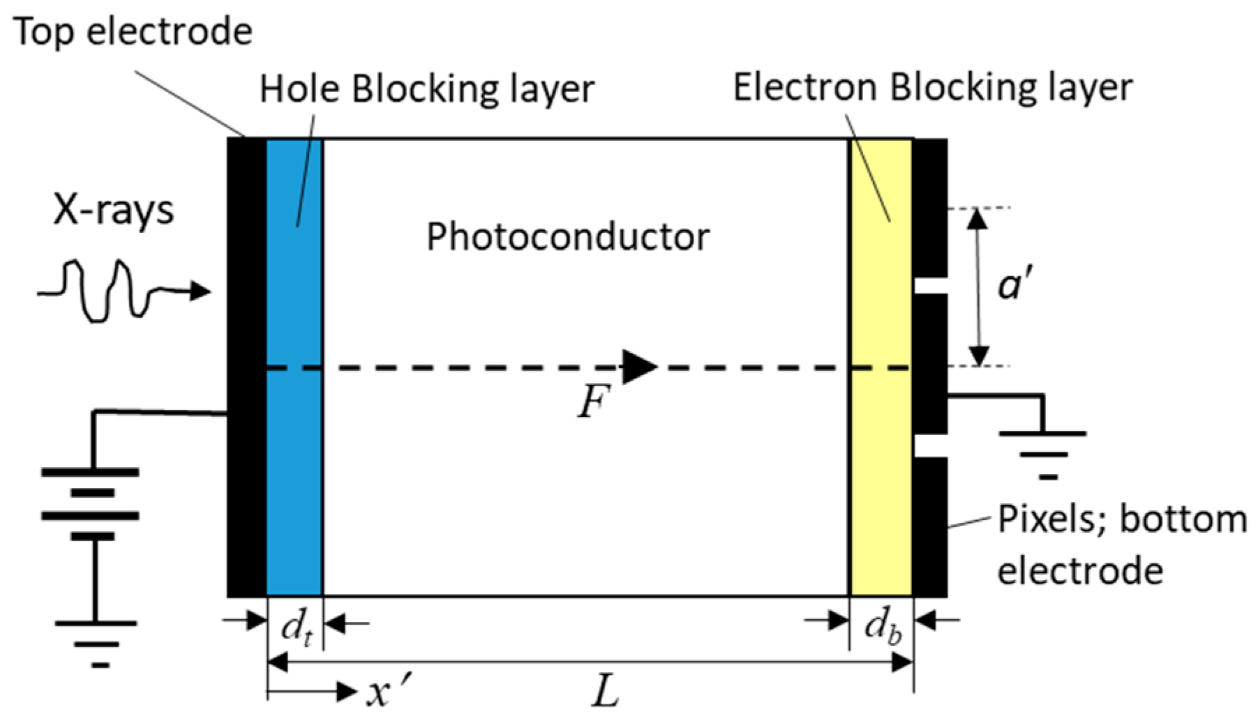
The cross-sectional structure of a multilayer imaging detector (i.e., the
n-
i-
p or
p-
i-
n photoconductor layer is sandwiched between two electrodes) is shown in
Figure 1, where
dt and
db are the thicknesses of the top and the bottom blocking layers, respectively. The top electrode is biased with a DC voltage source to establish a relatively strong electric field
F in the photoconductor layer. Note that the charge carriers drift along the
x′ direction, which induces the signal in the transverse directions at the electrodes. The X-ray generated electrons and holes drift across the photoconductor layer. Some of these carriers are trapped in the
i-layer and the rest are either trapped (or recombine with oppositely charged trapped carriers) in the blocking layers or reach at the corresponding electrode. The X-ray exposure rates used in diagnostic radiographic procedures (e.g., mammography or chest radiology) are relatively low and, thus, the charge carrier concentrations are also quite low [
10]. Therefore, the electric-field distribution across the photoconductor layer is almost constant (this is a valid assumption under small-signal analysis) [
11,
12]. Moreover, the diffusion current is negligible compared to its drift component because the applied field is quite strong [
13].
For a rotationally symmetric system, the MTF is also rotationally symmetric and can be expressed in terms of single spatial frequency, which is the Fourier transform of the line-spread function (LSF). In our previous publication [
14], we have formulated a generalized mathematical expression in integral form (Equation (19) of Ref. [
14]) from the first principle for calculating the Fourier transform of the LSF due to trapped charges in the single photoconductor layer, i.e., in metal/
i-layer/metal structure. In this paper, the generalized formulation is applied to a multilayer detector structure where the charge carrier transport properties of the different layers are different. The charge carrier trapping/recombination in the top blocking layer has a negligible effect on the signal spreading at the pixel/bottom electrode because this thin blocking layer is far from the pixel electrode. For simplicity, we can ignore the effect of the charge carrier trapping in the top blocking layer. However, the charge carrier trapping/recombination in the bottom blocking layer has a very significant effect on the signal spreading on the pixel electrodes and the image resolution. Following the formulation of Ref. [
14], the one-dimensional Fourier transform of the total line-spread function, considering the trapping in the bulk, as well as the blocking layer in the multilayer detector structure, can be written as follows:
where
qt(
x) is the normalized bulk trap carrier distribution in the
i-layer and
Qb is the normalized mean number of carriers that reach the photoconductor and bottom blocking layer interface. The charge carrier concentrations are normalized with respect to the total electron– hole pair (EHP) generation in the photoconductor per unit area. The distance coordinate is normalized with respect to the total photoconductor layer thickness
L (i.e.,
x =
x′/
L) and
d =
db/
L. The normalized spatial frequency
f =
f′ L, where
f′ is the actual spatial frequency (in mm
−1). The trap distribution profile across the blocking layer is unknown and, thus, the actual distribution of the carrier trapping/recombination rate within the blocking layer is unknown as well. For simplicity, an aggregate carrier loss can be calculated by assigning an average normalized carrier lifetime
τp in the blocking layer, where
τp =
μτ′pF/
L and
τ′p is the actual carrier lifetime in the blocking layer. Since the charge carrier trapping rate in the
i-layer is much lower than in the blocking layer and
d << 1, the normalized bulk trap carrier distribution,
qt(
x), can be written as follows [
7]:
The quantum efficiency η = 1 − exp(−1/Δ), normalized absorption depth Δ = 1/αL and normalized carrier lifetime τ = μτ′F/L, in which α is the linear attenuation coefficient of the photoconductor, μ is the effective drift mobility, and τ′ is the carrier lifetime. The subscripts t and b on τ refer to the charge carriers that drift towards the top and bottom electrodes, respectively. If the applied bias to the top electrode is positive, the subscript b represents holes (h) and t represents electrons (e), respectively. The polarity of the charge carriers drifting towards the bottom electrode is assumed to be positive in Equation (2).
The normalized mean number of carriers that reach the photoconductor and bottom blocking layer interface is written as follows [
7]:
Some of these carriers (i.e.,
Qb) are trapped or recombine in the blocking layer and the rest will reach the bottom electrode. It is important to note that, when a free carrier recombines with a trapped charge of the opposite sign, its effect on the overall MTF of the imager is the same as that of a free carrier being trapped [
14]. The first and second terms in Equation (1) represent the MTF due to bulk carrier trapping and recombination/trapping in the bottom blocking layer, respectively. The third term represents the relative number of carriers that reach at the pixel electrode and induce signal on the corresponding pixel only. When performing the integration of Equation (1), we get the following:
where ω = 2π
f. The expression for
G (
f = 0) is as follows:
The MTF is the unity at zero spatial frequency. Therefore, the MTF due to charge carrier trapping across the whole photoconductor layer is as follows:
If the blocking layer is absent in some of the X-ray detectors (i.e., d = 0), one can expect the bulk carrier trapping only and, in this case, MTFtr can be renamed as MTFb.
3. Presampling MTF
The effect of a digital detector on its image has been described as the following two-step processes: (i) the integration of the interacting input quanta in each element to produce a presampling detector signal, and (ii) the sampling of the presampling detector signal. In the spatial frequency domain, these two processes are described in terms of (i) presampling MTF, and (ii) aliasing as determined by the sampling spacing. Therefore, the shape of the presampling MTF contains all of the information on the signal blurring of the detector. The loss of resolution can occur in various independent stages in the detector system and the presampling MTF of an imaging detector is the product of the MTF of all of the independent stages. Thus, the presampling MTF is [
15] as follows:
where MTF
m =
ppeMTF
pe +
pkMTF
k +
pcMTF
c is the weighted MTF including the MTFs due to the range of the primary photoelectron,
K-fluorescence reabsorption, and Compton scattering; MTF
pe is due to the range of the primary photoelectron, MTF
k is due to the
K-fluorescence reabsorption, MTF
c is due to Compton scattering, MTF
tr is due to the charge carrier trapping, and
ppe,
pk, and
pc are the relative probabilities of the released charge carriers being from the photoelectric primary electron interaction,
K-fluorescent X-ray reabsorption, and Compton scattered photon, respectively. The signal blurring due to the range of primary photoelectron and Compton scattered photons are insignificant for diagnostic X-rays (up to 100 keV) [
12,
15] and, thus, MTF
m ≈
pkMTF
k. Therefore, the charge carrier trapping and the reabsorption of
K-fluorescent X-ray photons are the two dominant mechanisms that are responsible for the loss of resolution [
11,
16] in direct-conversion X-ray detectors.
The MTF due to the reabsorption of
K-fluorescent X-rays (to get the usual unity normalization of the MTF at zero frequency) [
17] is as follows:
where,
and,
Here, J0 is the zero order Bessel function and αk is the linear attenuation coefficient of the K-fluorescent X-rays.
The signal integration on each pixel causes a loss of resolution due to averaging the signal over a pixel area. The smaller the pixel size, the better the resolution. For square pixels with dimension
a (a = a′/L), the following can be considered:
4. Results and Discussions
The presampling MTF performance of the a-Se detectors were examined for chest radiographic and mammographic applications. In order to avoid unnecessary complex calculations, the average energy of the incident spectra was used in this paper. The effective drift mobility of electrons and holes in a-Se was assumed as 0.003 and 0.12 cm2/V-s, respectively.
The MTF model was fitted to the published experimental data on a-Se detectors for chest radiographic applications.
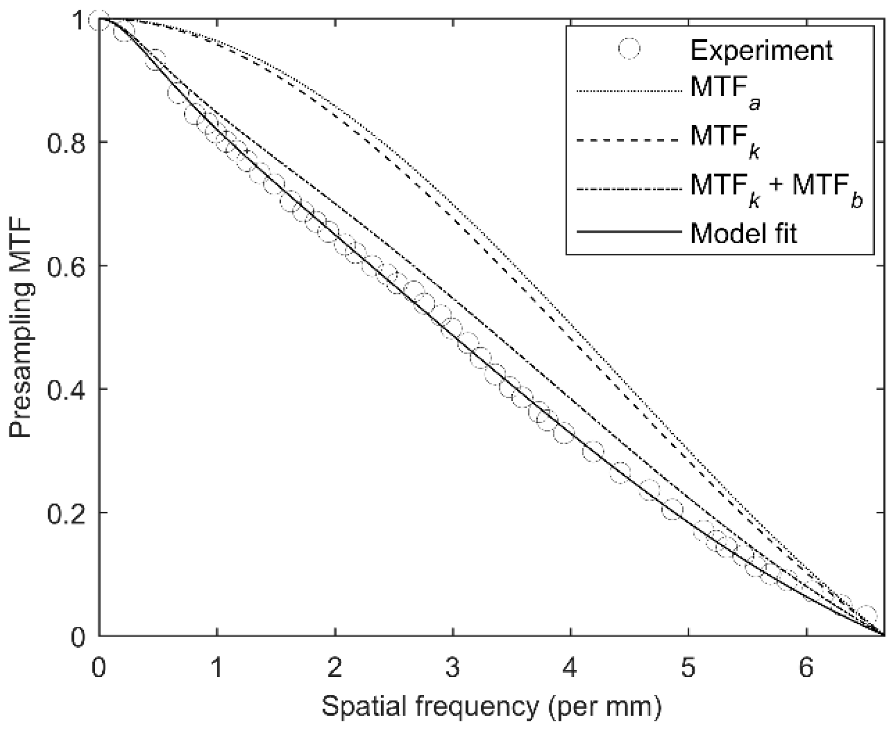
Figure 2 shows the MTF(
f) as a function of spatial frequency for a chest radiographic a-Se detector. The experimental data have been extracted from Figure 7 of Ref. [
18]. This 1 mm thick detector was exposed to 75 kVp X-ray exposure with 39.7 mm Al filtration. A negative bias voltage was applied in order to create an electric field of 10 V/μm in the photoconductor layer [
18]. The average photon energy was 59 keV for 75 kVp with 39.7 mm Al filtration X-ray spectra. The bottom blocking layer thickness,
db = 15 μm and pixel size,
a′ = 150 μm. The open circles, dotted, dashed, dash-dotted, and solid lines represent the experimental data, the aperture MTF, the presampling MTF considering
K-fluorescence reabsorption, the presampling MTF considering
K-fluorescence reabsorption and bulk trapping (MTF
b), and the overall presampling MTF (Equation (7)) model fit to the experimental data, respectively. There was a good agreement between the theoretical model and the experimental data by adjusting the carrier lifetimes,
τp = 0.01,
τ′e = 250 μs, and
τ′h = 5 μs. All of these values are reasonable for
a-Se [
4]. The normalized lifetimes were
τb = 0.6,
τt = 0.75, and
τp = 0.01. Note that the trap concentration in the blocking layer was two to three orders of magnitude larger than that in the bulk a-Se layer [
19,
20]. The difference between the dotted and dashed lines represents the effect of
K-fluorescence reabsorption, which is very small because the average photon energy (59 keV) was much higher than the
K-edge (12.5 keV in
a-Se) energy. The difference between the dashed and dash-dotted lines represents the effect of the bulk charge carrier trapping on presampling MTF, which showed to be the most significant for a-Se chest radiographic detector. The trapping/recombination in the bottom blocking layer had the next most significant effect on the overall MTF. In summary, the charge carrier trapping/recombination (in both the bulk and the blocking layer) mostly determined the resolution of the amorphous selenium chest radiographic detectors.
The MTF model was applied to the
a-Se-based mammographic detectors.
Figure 3 shows the presampling MTF(
f) as a function of the spatial frequency for a negatively biased
a-Se detector of 200 μm thickness at 28 kVp (tungsten anode) X-ray exposure with 2.5 mm Al filtration. The applied electric field
F = 10 V/μm and the average photon energy was 22.3 keV. The pixel size,
a′ = 85 μm. The open circles, dotted, dashed, dash-dotted, and solid lines represent the experimental data, the aperture MTF, the MTF considering
K-fluorescence reabsorption, the MTF considering
K-fluorescence reabsorption and bulk trapping, and the overall presampling MTF model fit to the experimental data, respectively. The experimental data have been extracted from Ref. [
8]. The theoretical model fit well with the experimental data with
db = 6 μm,
τp = 0.02,
τ′e = 250 μs, and
τ′h = 5 μs, which are very reasonable values for
a-Se, as mentioned above. The
K-fluorescence had a significant effect on the MTF because the average photon energy (22.3 keV) was very close to the
K-edge. The charge carrier trapping/recombination in the blocking layer had the next most significant effect on MTF at the Nyquist frequency (5.88 mm
−1), as is evident from the difference between the solid and the dash-dotted lines. The bulk trapping had less of an effect because of the relatively thinner photoconductor layer and, hence, there was a lower trapping rate in the bulk. In summary, the charge carrier trapping/recombination in the blocking layer and
K-fluorescence reabsorption mainly controlled the resolution of the amorphous selenium mammographic detectors.
The loss of resolution due to trapping/recombination in the blocking layer depended on the thickness and the average carrier lifetime in the blocking layer.
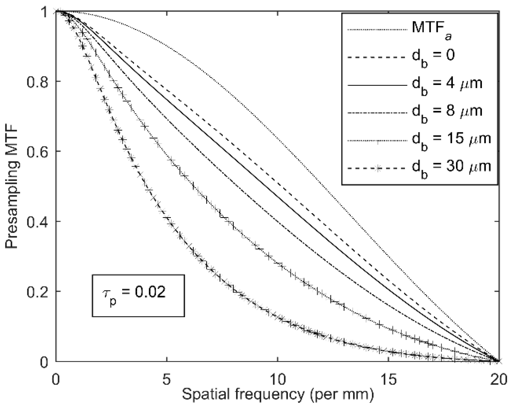
Figure 4 and
Figure 5 show the effects of the thickness and the average carrier lifetime in the blocking layer in a-Se mammographic detectors. The applied electric field
F = 10 V/μm, the average photon energy was 22 keV,
L = 200 μm, and
a′ = 50 μm. The MTF at Nyquist frequency (10 mm
−1) degraded almost proportionately with the blocking layer thickness. The blocking layer had almost no effect on MTF when
τp was larger than the unity. On the other hand, the effect of the blocking layer saturated when
τp was less than 0.001 (i.e., no further degradation of MTF if
τp was less than 0.001). As is evident from
Figure 4 and
Figure 5, the blocking layer thickness had a more profound effect on the resolution than the average carrier lifetime in the blocking layer. In other words, the blocking layer thickness had a more significant effect on the resolution than the number of trap centers in the blocking layer.


