Article

Different Switching Strategy for a Quadratic Boost Converter Based on Non-Series Energy Transfer (QBC-NSET)


by
Luis Humberto Diaz-Saldierna
1,*,
Julio C. Rosas-Caro
2,*,
Jesus Leyva-Ramos
1,
José G. González-Hernández
3,4,
Francisco Beltran-Carbajal
5 and
Johnny Posada
6
1
Instituto Potosino de Investigación Científica y Tecnológica, Camino a la Presa San José No. 2055, San Luis Potosí 78216, Mexico
2
Facultad de Ingenieria, Universidad Panamericana, Alvaro del Portillo 49, Zapopan 45010, Mexico
3
Tecnológico Nacional de México/Instituto Tecnológico de Ciudad Madero, Av. Primero de Mayo, Ciudad Madero 89440, Mexico
4
Mechatronics and Renewable Energy Department, Universidad Tecnológica de Altamira, Altamira 89608, Mexico
5
Departamento de Energía, Unidad Azcapotzalco, Universidad Autónoma Metropolitana, Azcapotzalco, Mexico City 02128, Mexico
6
Grupo de Investigación en Energías—GIEN, Facultad de Ingeniería y Ciencias Básicas, Universidad Autónoma de Occidente, Cali 760001, Colombia
*
Authors to whom correspondence should be addressed.
Electricity 2026, 7(2), 31; https://doi.org/10.3390/electricity7020031
Submission received: 7 February 2026 / Revised: 26 March 2026 / Accepted: 30 March 2026 / Published: 2 April 2026

Abstract

This paper explores a new switching strategy for a recently proposed quadratic boost converter. The topology under study is a high-step-up DC–DC converter with a configuration that allows a portion of the processed energy to be used in what we call a non-series transfer. This characteristic reduces the amount of power processed redundantly. This converter, called a Quadratic Boost Converter based on Non-Series Energy Transfer (QBC-NSET), also has a non-pulsating input current, which is especially desirable for applications like photovoltaic and fuel-cell sources. This paper proposes a different switching strategy that reduces the output voltage ripple without increasing the switching frequency and without increasing the stored energy (inductance in inductors or capacitance in capacitors). The converter has two transistors, originally operated with synchronized signals; the proposed strategy provides independent switching signals with a phase shift between them. This enables the output capacitor to charge in a different switching state, producing a smaller voltage ripple while preserving the advantages of the topology originally presented. Steady-state analysis and voltage gain derivations confirm that the fundamental conversion characteristics remain unchanged. Experimental results obtained from a laboratory prototype validate the effectiveness of the proposed approach, demonstrating the reduction in the output voltage ripple.

1. Introduction

Renewable energies have recently been attracting attention due to several factors that could accelerate their adoption. One of these factors is the technological advancement in technologies like photovoltaic (PV) systems and energy storage systems. Innovations in photovoltaic materials have resulted in higher efficiencies and lower production costs [1,2]. Additionally, ongoing improvements in inverter technologies and hybrid systems have enhanced the grid integration of renewable energy, enabling better management of power output and storage [3,4]. Such advancements are critical as they enable broader access to solar energy for both residential and commercial users, facilitating widespread adoption across various sectors [5]. Another factor is government policies and incentives; several countries have implemented incentives to encourage investments in renewable energy [6,7,8]. All this is strongly motivated by rising environmental awareness, concerns regarding climate change, and the environmental impact of fossil-fuel-based power generation [9,10].
Renewable energy sources are characterized by their open range operation rather than having a particular constant output voltage; furthermore, they may be unpredictable due to fluctuating weather conditions and varying load demands [11]. Power conditioning enables the integration of energy storage, which is crucial for maintaining DC-link voltage stability and addressing common challenges associated with integrating variable generation into utility grids [12].
On the other hand, a pulsating current in power-electronic interfaces accelerates the degradation of some power sources, which include renewable sources, which is why many renewable energy systems (RES)-oriented converter topologies are designed with continuous (non-pulsating) input current [13,14,15,16]. Switching ripple increases the RMS currents from the RES, inducing additional losses and thermal stresses [17,18,19,20].
These are the reasons why the development of DC–DC converters for RES applications with high gains and continuous input current ripple is highly desirable.
The conventional boost converter has continuous input current, which can be adjusted by selecting an adequate inductor. It is theoretically able to raise voltage by increasing the duty ratio, but in practice, high voltage gain (like the one used in RES applications) in practice requires high duty cycles, which degrade efficiency due to increased conduction losses and worsen transient behavior [21,22,23]. This high duty cycle operating region is one of the main reasons why traditional boost topology variants cannot satisfy modern high step-up requirements in modern systems [24,25].
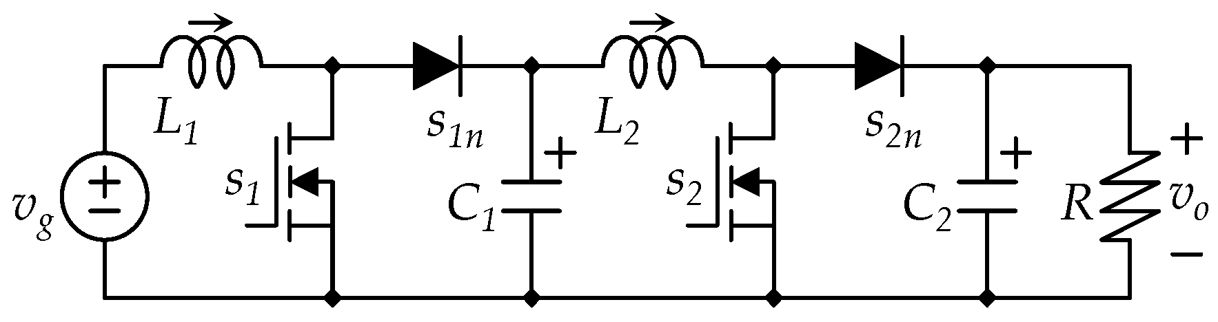
Several configurations have been explored to achieve high voltage gain with continuous input current. One option is to connect two boost converters, one after the other, in what we call a cascaded connection, see Figure 1. This connection allows for an increase in the voltage gain. The operation of this system is simple and effective; it contains two transistors, and the energy is transferred in what we call a series transference.
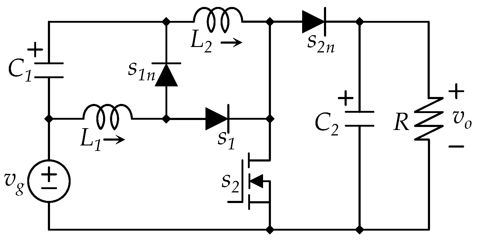
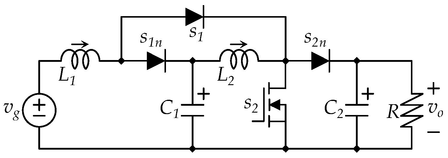
One contribution that can be considered an improvement of the converter in Figure 1 is what we now call the traditional quadratic boost converter (see Figure 2), initially proposed in [26]. It contains one transistor and three diodes; it is also an effective converter, and several research works have focused on this topology [26,27,28].
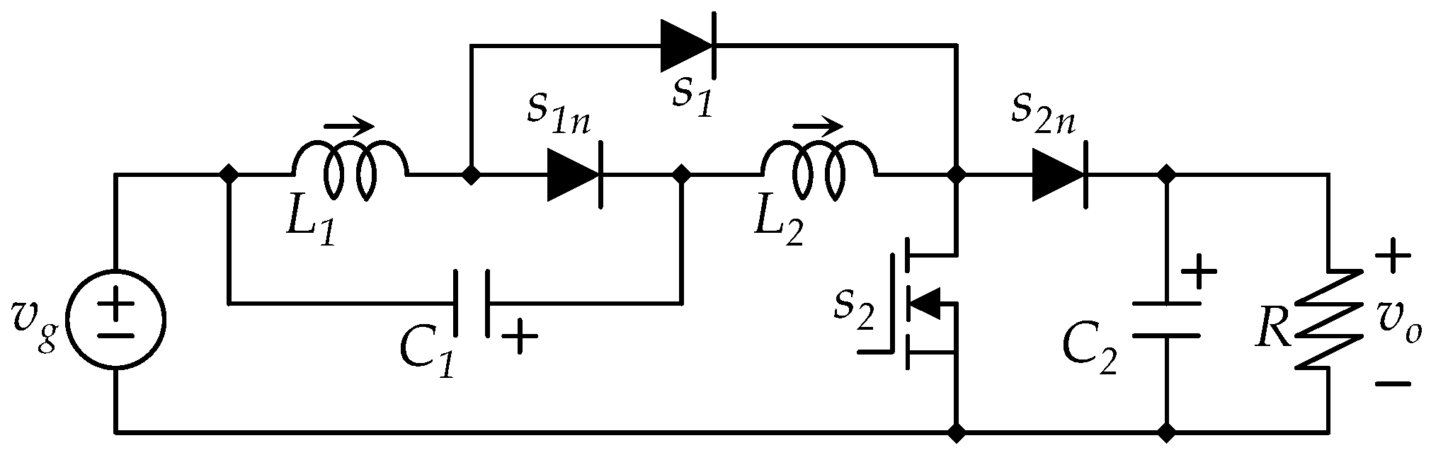
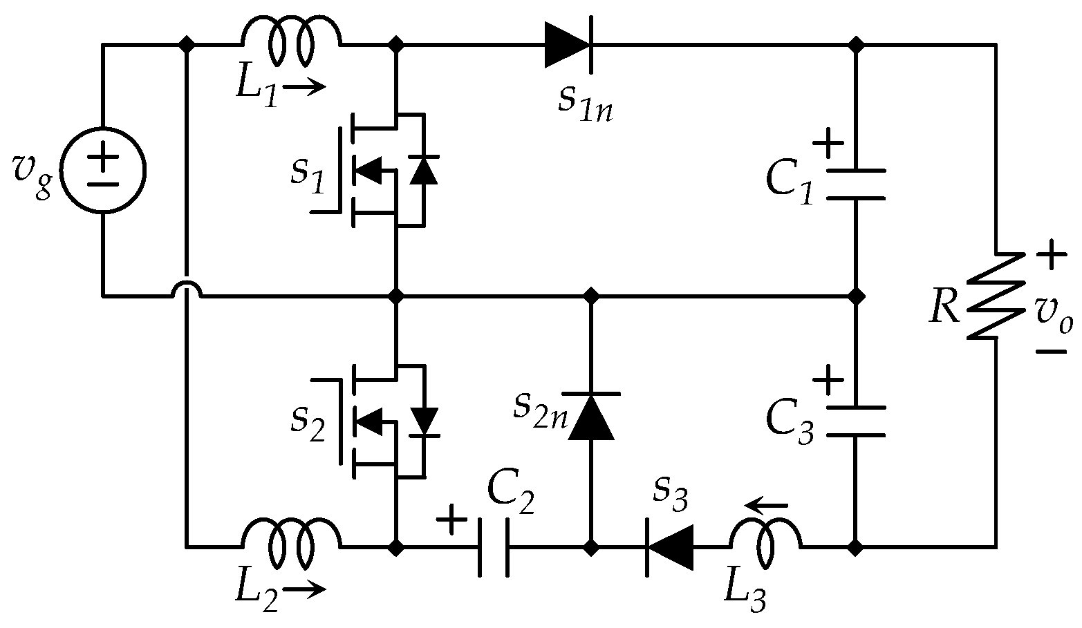
Recent QBC developments remain transformer-less/non-isolated while preserving the quadratic-gain principle [27,29,30,31]. Another recently studied converter is the quadratic boost converter with low buffer capacitor stress [32,33], see Figure 3. It is similar to Figure 1, with the advantage that C1 sustains less voltage, and the drawback that the input current becomes discontinuous.
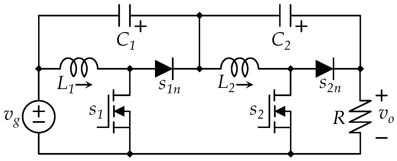
Figure 4 shows the low energy storage quadratic boost converter (LES-QBC) [34,35], another quadratic boost converter in which the capacitor stores low energy since it is rated to a reduced voltage compared to other topologies; on the other hand, the input current is discontinuous.
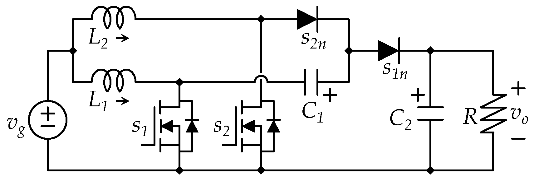
Another two boost converters with quadratic gain were studied in [36]. Figure 5 shows the Modified Quadratic Boost converter, a quadratic converter in which C1 has reduced energy stored since it has less voltage, which leads to a smaller-sized capacitor.
Figure 6 shows the quadratic boost converter proposed in [36] as a Single-Switch Quadratic Boost (SSQB) converter.
In the aforementioned converters, we can comment on the following characteristics:
(i) 
Two converters have continuous input current, while the others have discontinuous input current. In this case, the cascaded boost and the traditional quadratic boost have an input inductor whose current is equal to the input current. This allows the input current to be non-pulsating, but the input current ripple can also be established by an adequate selection of the input inductor.
(ii) 
Three converters have a single transistor: the traditional quadratic boost and the quadratic boost with low buffer capacitor stress. In those cases, there is a single switching signal. The other three converters have two transistors; still, the converters can operate with a single switching signal if both transistors are operated synchronously, or each of them may have an independent switching function.
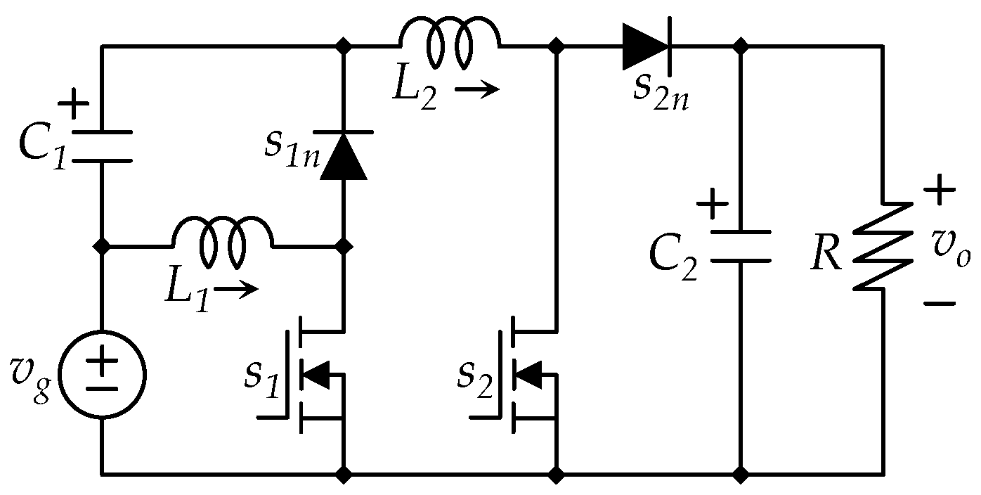
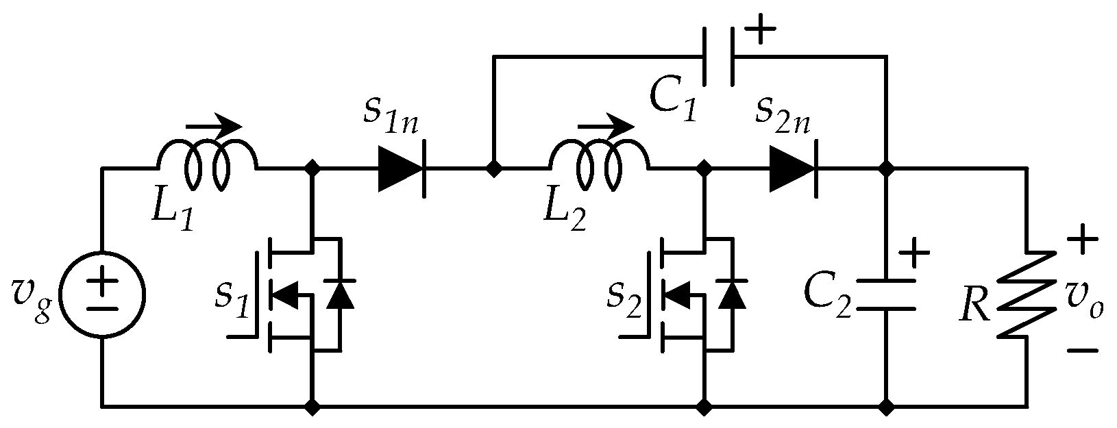
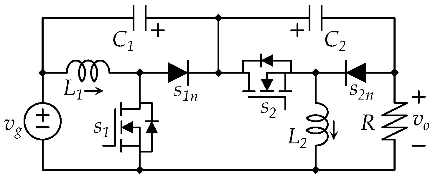
One of the most recent contributions addressing high step-up DC–DC conversion is presented in [37], see Figure 7. This converter was called the Quadratic Boost Converter based on Non-Series Energy Transfer (QBC-NSET). A two-transistor converter with continuous input current (it was an input inductor). Their main characteristic is the connection of a capacitor that allows a portion of the processed energy to be in what we call non-series transfer. The converter was proposed in [37] to operate with a single switching function.
The QBC-NSET reduces the amount of power processed in a redundant manner. By employing a transfer capacitor that enables parallel power flow between stages. Similar to the other discussed converters, the converter achieves a quadratic voltage gain while avoiding excessive energy reprocessing. Additionally, the topology features a common ground, a non-pulsating input current—highly desirable for several applications.
The similarities among the discussed converters allow us to observe that some research efforts on quadratic boost converters have focused on improvements based on structural or topological modifications. Less attention has been devoted to exploring alternative switching strategies in multi-switch quadratic configurations as a means to improve output voltage quality without altering the hardware structure, switching frequency, or the component values.
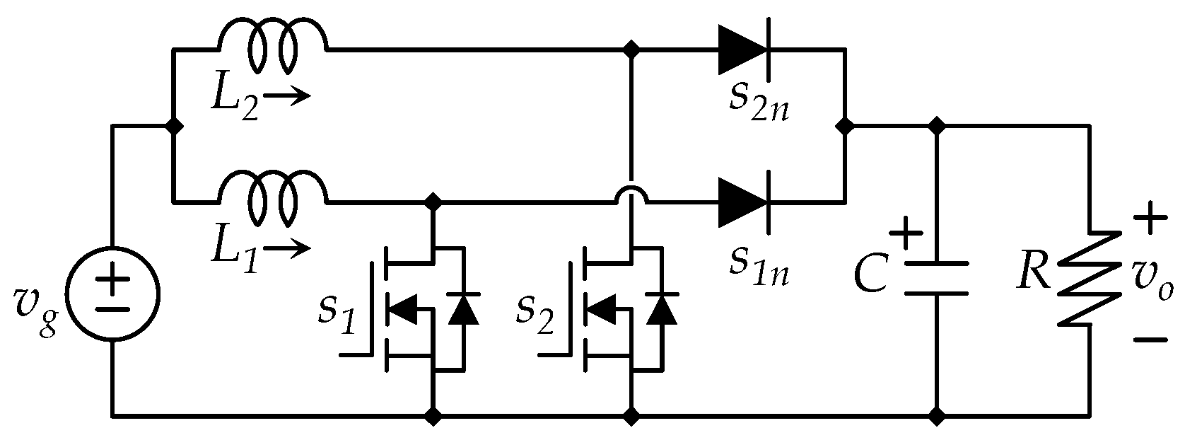
On another topic, there is an expansion technique that can be applied to almost all topologies called the interleaved connection or multiphase converters. Figure 8 shows the interleaved boost converter.
In interleaved converters, multiple power stages operate in parallel. The advantage of that technique is that the multiple phases share the dissipated power among them, allowing a power rating expansion with low-power devices.
Interleaved topologies use phase-shifted switching signals, resulting in a low input current ripple compared to the current ripple in each inductor, which is due to a partial cancellation of the inductor current ripple. The input current in Figure 8 is equal to the sum of the currents through both inductors. This effect introduced a second alternative to reduce input current ripple in some topologies, beyond simply increasing inductance values. Furthermore, the output voltage ripple in Figure 8 is lower than that with the same capacitance in a single-phase converter because diodes activate at different times, doubling the frequency of the current through the capacitor.
Similar to the interleaved topologies, there are modern topologies with two input inductors, in which the input current ripple can be reduced through current ripple cancellation. Figure 9 shows the input parallel output series connection of a boost converter and a high voltage three-switch converter [38]. Two different switching strategies have been investigated for that converter [38].
Another example of the input current ripple cancellation is the series capacitor boost converter [39], see Figure 10. In this converter, the input stage resembles the interleaved boost converter, and switching ripple cancellation techniques can be applied to reduce the input current ripple [39].
The interleaving technique has been employed in several topologies, mainly to reduce the input current ripple. In the case of a non-interleaved converter, for example, in cascaded types of converters, like the one shown in Figure 1, Figure 2, Figure 3, Figure 4, Figure 5, Figure 6 and Figure 7, some similar ideas have been applied to reduce the output voltage ripple.
Figure 11 shows a buck–boost converter presented in [40] in which a switching technique similar to the one proposed in [39] was applied to reduce the output voltage ripple.
The technique proposed in [39] consists of having different duty cycles in each transistor, a proportional relationship between the duty cycles, and a proportional difference between the inductors. The technique proposed in [40] consists of having different capacitors and calculating them according to an equation that defines in which duty cycle the output voltage ripple is desired to be zero.
Another example with another buck–boost converter was proposed in [41], in which a modified non-inverting step-down/up (MNI-SDU) converter is operated with a modified switching strategy based on a parameter λ that introduces a phase shift between the switching signals. This parameter can be adjusted to minimize the output voltage ripple [41].
The QBC-NSET topology proposed in [37] presents an interesting opportunity in this regard. Since the converter contains two active switches operated synchronously, the existence of two controllable devices allows for exploring alternative modulation schemes. Nevertheless, the impact of independent gating signals on the internal energy transfer mechanism and on the output voltage ripple has not been previously investigated.
This observation motivates the present work. Rather than proposing a new topology, this paper explores whether a different switching strategy applied to the recently published QBC-NSET can enhance its performance, specifically in terms of output voltage ripple reduction, while preserving its intrinsic advantages such as quadratic voltage gain, non-series energy transfer, and continuous input current. By identifying this modulation-based opportunity, the work addresses this gap.
This paper explores an alternative switching strategy for the converter proposed in [37], which can be called the Quadratic Boost Converter based on Non-Series Energy Transfer (QBC-NSET). The converter has two transistors, and it was proposed to operate them with synchronized gating signals. This work explores the use of independently timed switching signals. Specifically, both switches operate with the same duty cycle D, and the second gating signal is delayed by half of the switching period (TSW/2) with respect to the first. Therefore, the switching functions are identical in shape and width, but temporally displaced by TSW/2. This different operating mode enables other switching states to appear during the operation, which brings an advantage. The operation of the converter remains the same, but the output voltage ripple is smaller compared to the previous strategy. This is achieved without increasing the switching frequency or requiring additional passive energy storage (without increasing the inductance in inductors or the capacitance in capacitors). The proposed strategy preserves the intrinsic advantages of the original converter, including its quadratic voltage gain, non-series energy transfer mechanism, and non-pulsating input current.
The article presents a steady-state analysis to demonstrate that the fundamental conversion characteristics remain unchanged. Furthermore, a comparative assessment of the synchronized and proposed switching strategy is presented in terms of voltage gain, current, voltage stress on passive and active components, and output voltage ripple. The effectiveness of the proposed approach is experimentally validated using a laboratory prototype.

2. The QBC-NSET in Its Original Switching Strategy

Figure 7 illustrates the QBC-NSET considered in this work. The topology consists of two switching stages sharing a common ground and interconnected through a transfer capacitor that enables parallel energy flow between the intermediate stage and the output. The first stage is formed by the inductor L1, the switch s1, and the diode s1n, while the second stage includes the inductor L2, the switch s2, the diode s2n, and the output capacitor C2. Unlike conventional cascaded quadratic boost converters, the QBC-NSET has the intermediate capacitor C1.
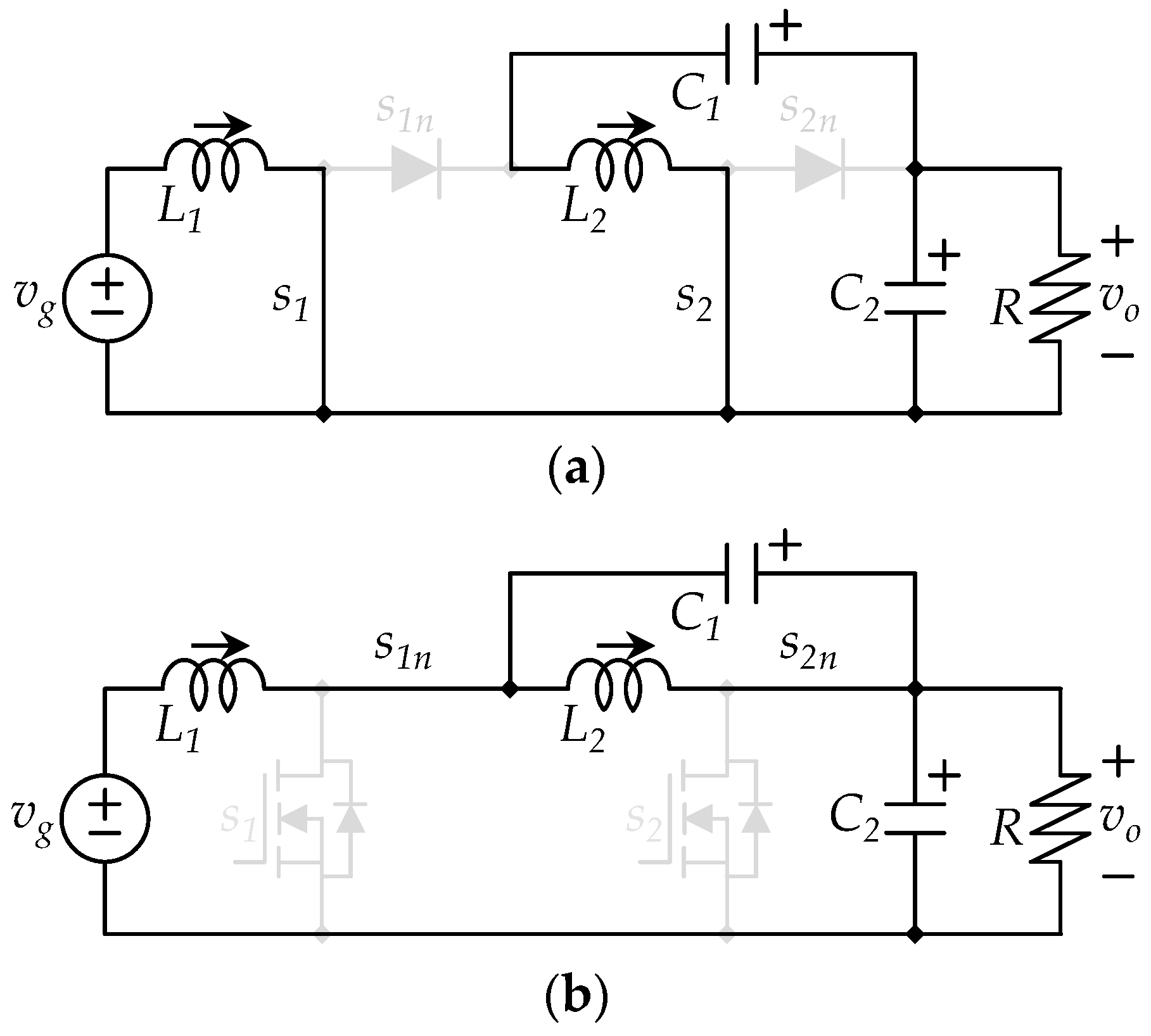
The QBC-NSTE has two transistors; it was originally introduced in [37] with a synchronized gating scheme applied to them. Under this approach, both switches are driven using the same duty cycle and commutate simultaneously within each switching interval. As a result, the converter behavior in continuous conduction mode (CCM) can be described by two switching states, as shown in Figure 12.
The first switching state corresponds to the interval in which both switches are on (see Figure 12a) while the diodes are off, whereas the second switching state occurs when the switches are off (see Figure 12a), and the current is transferred through the diodes.
Before presenting the averaged model, it is important to clarify the assumptions under which the state-space averaging approach is valid. The analysis presented in this work assumes operation in continuous conduction mode (CCM), ideal switching behavior within each switching interval, and a switching frequency at least one order of magnitude higher than the dominant converter dynamics (e.g., fsw ≥ 10 times the dominant pole frequency or control bandwidth). This condition ensures proper time-scale separation and allows the averaged model to represent the low-frequency behavior of the converter without being affected by switching harmonics. The state-space averaging method, therefore, provides an accurate representation of the converter’s low-frequency (mean) behavior.
It should be noted that the averaged model does not capture high-frequency switching dynamics and may lose accuracy under large-signal transients or if the converter operates in Discontinuous Conduction Mode (DCM). Nevertheless, for steady-state analysis and ripple comparison under CCM operation, the averaged model constitutes a valid and widely accepted analytical tool.
Based on the derived operating states and using a conventional averaging approach, the converter’s mean dynamic behavior can be represented by the following system of differential equations.
L 1 d i L 1 d t = d v g + 1 d v g + v C 1 v C 2 .
L 2 d i L 2 d t = d v C 2 v C 1 + 1 d v C 1 .
C 1 d v C 1 d t = d i L 2 + 1 d i L 2 i L 1 .
C 2 d v C 2 d t = d i L 2 i o + 1 d i L 1 i o .
With iL1 and iL2, the currents flowing through inductors L1 and L2, respectively, the variables vC1 and vC2 correspond to the voltages across capacitors C1 and C2. The input source voltage is given by vg, the output current is represented by io, and d denotes the duty ratio. The set of Equations (1)–(4) may then be simplified as:
L 1 d i L 1 d t = v g + 1 d v C 1 v C 2 .
L 2 d i L 2 d t = d v C 2 v C 1 .
C 1 d v C 1 d t = i L 2 1 d i L 1 .
C 2 d v C 2 d t = 1 d i L 1 d i L 2 i o .
The set of Equations (5)–(8) represents the dynamic model of the converter, which can be used to obtain the steady-state by imposing that the time derivatives are zero. Accordingly, the resulting set of equilibrium relationships is given in Equations (9)–(12). For clarity, steady-state quantities are distinguished from their dynamic counterparts by adopting uppercase notation for the corresponding variables, as defined below.
V C 2 = V g 1 1 D 2 .
V C 1 = V g D 1 D 2 .
I L 1 = I o 1 D 2 .
I L 2 = I o 1 D .
For sizing the passive components (inductors and capacitors), let us use the approach of defining an allowable peak switching ripple level, which must be previously specified. For the inductor current, we can call the current ripples as ΔiL1 and ΔiL2, similarly, the voltage ripple for the capacitor voltages can be called ΔvC1 and ΔvC2. The switching frequency is called fsw, and the switching period (the inverse of the switching frequency), can be called Tsw. Once the ripple constraints are defined, the corresponding values of the inductors L1 and L2 and the capacitors C1 and C2 can be determined based on the steady-state ripple expressions. The following expressions were calculated in the operating interval when the switches are on, and then with the switching state shown in Figure 12a.
Δ i L 1 = D V g 2 L 1 f s ω .
Δ i L 2 = D 2 L 2 f s ω V C 2 V C 1 = V g 2 L 2 f s ω D 1 D .
Δ v C 1 = D 2 C 1 f s ω I L 2 = I o 2 C 1 f s ω D 1 D .
Δ v C 2 = 1 D 2 C 2 f s ω I L 1 I o = I o 2 C 2 f s ω 1 ( 1 D ) 2 1 D .
The number two in the denominator comes from the convention that the switching ripple is defined as half of the peak-to-peak change in each variable. It means the ripple is measured from the average value of the state variable to its maximum deviation.
The first three energy storage elements (L1, L2, and C1) are being charged during the switching state in which transistors are on, and diodes are off, as shown in Figure 12a. The capacitor C2 is getting charged in the other state (when transistors are off), as shown in Figure 12b. That is why the time (1−D)Tsw is associated with its calculation.
The output voltage ripple is identical to the voltage ripple across C2. This distinction is crucial, as the present work focuses on a switching scheme specifically designed to reduce the converter’s output voltage ripple.
Δ v o = Δ v C 2 = I o 2 C 2 f s ω 1 ( 1 D ) 2 1 D .
Let us see a bit more in detail the voltage ripple in C2, which is the output voltage ripple, since it is the main advantage of the proposed operation. In this operation, we have two equivalent circuits. When the transistors are closed (diodes are open) during a time dTsw, the converter operates as in Figure 12a; when the transistors are open (diodes are closed) during a time (1D)Tsw, the converter operates as in Figure 12b.
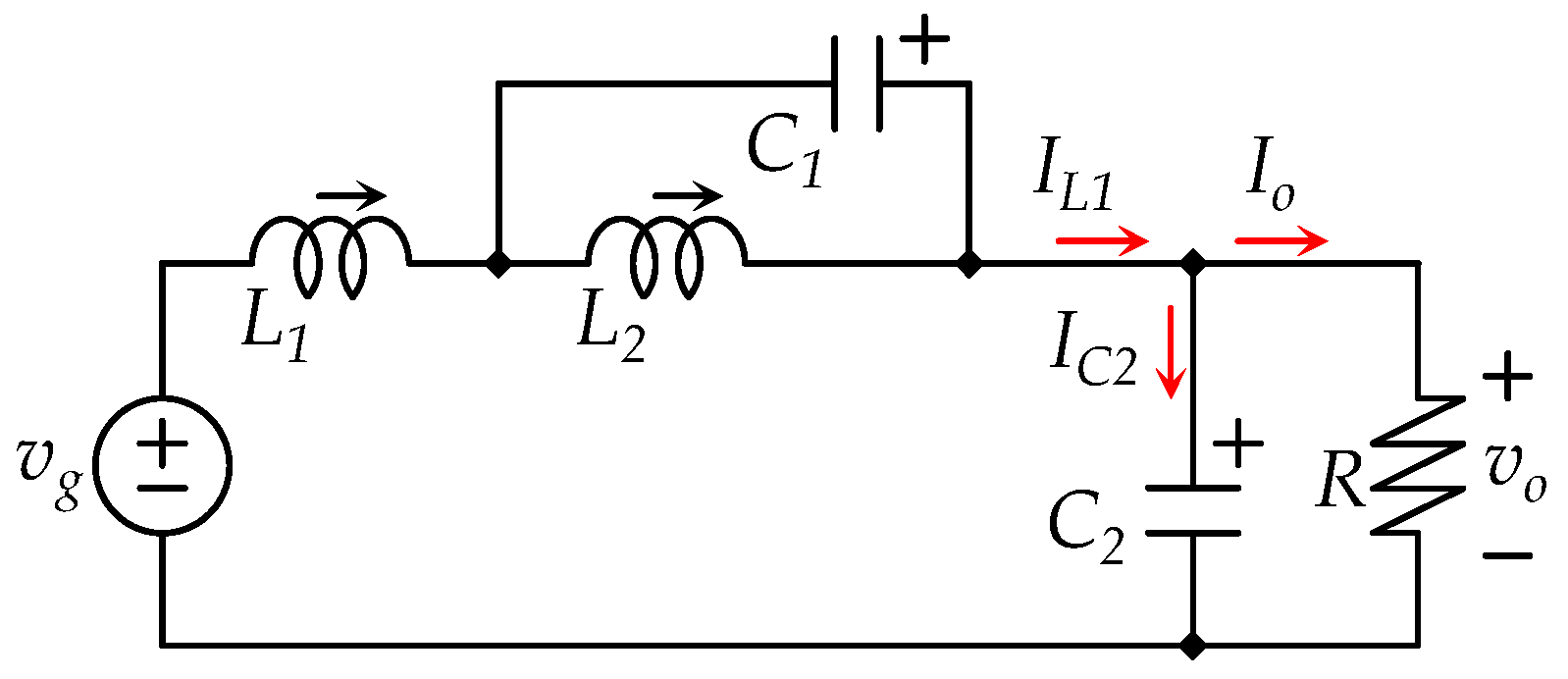
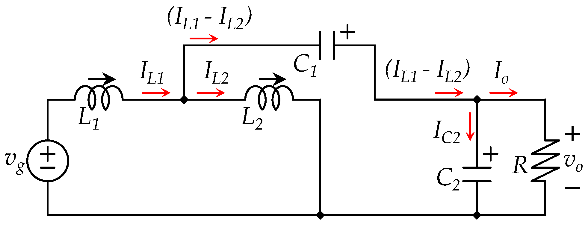
We choose the second case (Figure 12b) to calculate Equation (16). Figure 13 shows the circuit equivalent to Figure 12b; the current through C2 is marked in the equivalent circuit. We can see L2 and C1 can be seen as a super-node, and then the current that departs from the super-node is the same as that that enters (IL1). In this equivalent circuit, the current through C2 is equal to IL1-Io, and the time it lasts is (1D)Tsw. From the mentioned current and time, the voltage ripple across capacitor C2 was expressed as (16).

3. The QBC-NSET with the Proposed Switching Strategy

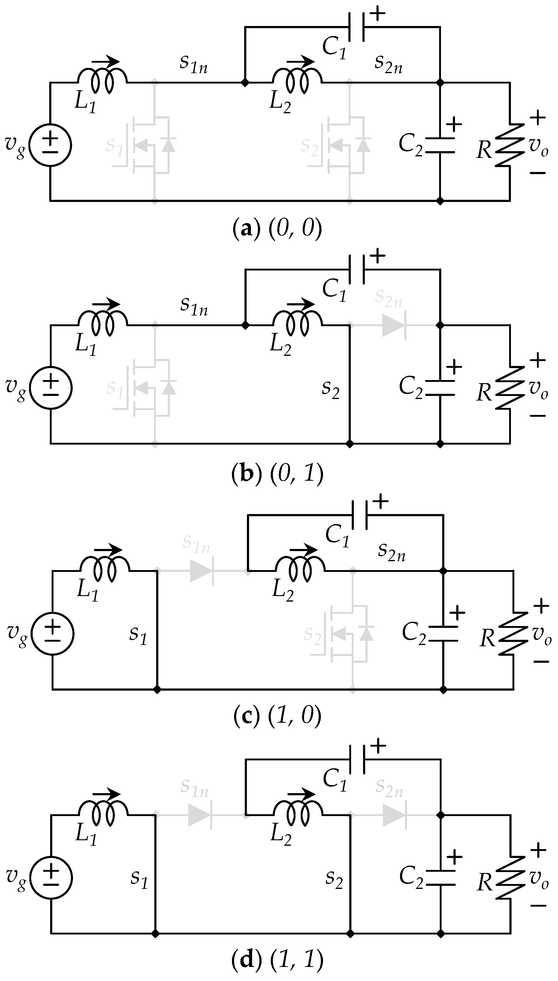
This section introduces the proposed switching strategy, in which the active switches are no longer driven in a synchronized manner. The proposed strategy allows each switch to be independently driven. This independent operation allows any of the four possible binary combinations of switching signals to appear; see the possible combinations in Figure 14.
Specifically, in the proposed strategy, both switches operate with the same duty cycle D, and the second gating signal is delayed by half of the switching period (TSW/2) with respect to the first. Therefore, the switching functions are identical in shape and width, but temporally displaced by TSW/2.
The proposed operation of the converter now has four possible switching states (instead of two), since there are now two independent switching signals, s1 (with s1n as its complementary signal) and s2 (with s2n as its logical complement). The four possible switching states correspond to the combinations of the conduction states of (s1, s2). These possibilities are (0, 0), (0, 1), (1, 0), and (1, 1), where each pair represents the on/off condition of the first and second switches, respectively.
Before proceeding with the system-level modeling, it is important to note that although four switching states are theoretically possible, not all of them necessarily occur within a single switching period. The actual sequence of switching states depends on the selected duty ratios. As a result, the converter can operate under two different operating modes: (i) when the duty ratio is greater than 0.5, (ii) when the duty ratio is lower than 0.5. The case when d = 0.5 is a particular case of any of the two previous cases and coincides with the traditional operation also.

3.1. Duty Cycle d > 0.5

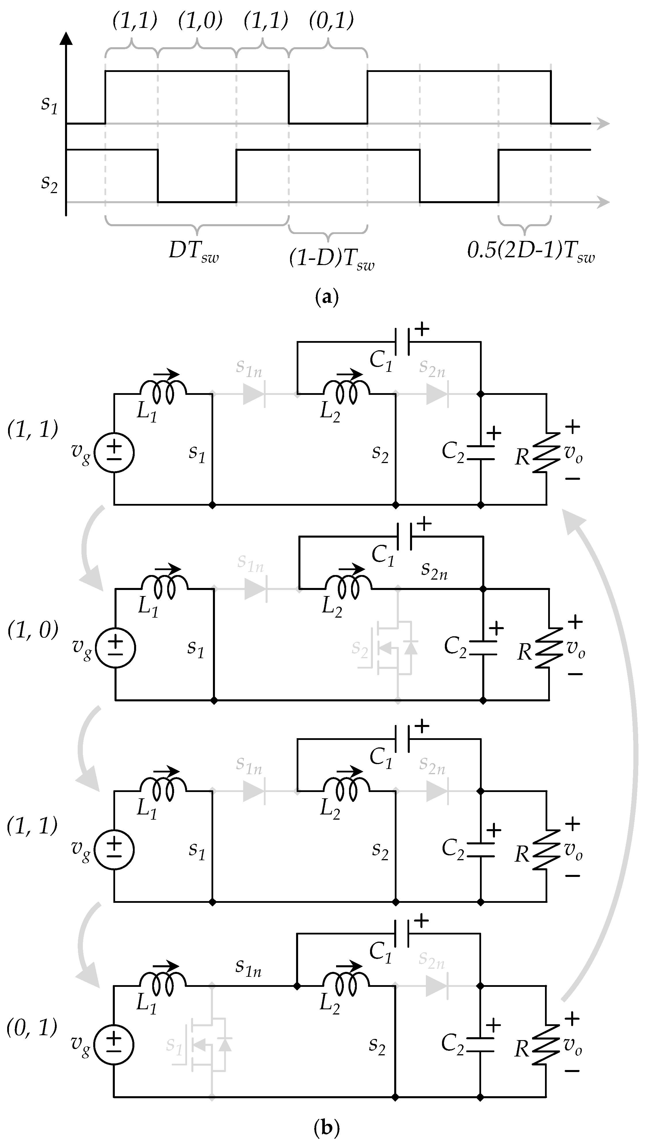
Figure 15a shows the switching signals of the converter when D > 0.5; for example, the duty cycle is 0.7, and the signals are shifted by half of the switching period (Tsw/2). We can see the switching state (0, 0) never appears; due to the signal’s width, there is an overlap in which the switching state (1, 1) shows twice in a switching cycle. If we take one switching cycle for analysis, we can see the sequence of switching states is (1, 1), (1, 0), (1, 1), and (0, 1). Figure 15b shows the sequence of switching states, which is useful to understand the average of signals.
In this case, we still can use the averaging technique, but in this case, we must observe that the switching period is not split into two different times like in the previous strategy, and in the traditional averaging technique, in which the switching period is divided into the active state dTsw, and the complementary state (1−d)Tsw.
In this case, the switching period is divided into four sub-periods, as shown in Figure 15, the first switching state (1, 1) remains a time 0.5(2d−1)Tsw, followed by the state (1, 0), which remains for a time (1−d)Tsw, the third time corresponds again to the state (1, 1), and remains again a time 0.5(2d−1)Tsw, and the last switching state (0, 1), remains also a time (1−d)Tsw.
The average voltage across inductors L1 and L2, and the average current through capacitors C1 and C2, would be as shown in Equations (18)–(21).
L 1 d i L 1 d t = 0.5 2 d 1 v g + 1 d v g + 0.5 2 d 1 v g + 1 d v g + v C 1 v C 2 .
L 2 d i L 2 d t = 0.5 2 d 1 v C 2 v C 1 + 1 d v C 1 + 0.5 2 d 1 v C 2 v C 1 + 1 d v C 2 v C 1 .
C 1 d v C 1 d t = 0.5 2 d 1 i L 2 + 1 d i L 2 + 0.5 2 d 1 i L 2 + 1 d i L 1 i L 2 .
C 2 d v C 2 d t = 0.5 2 d 1 i L 2 i o + 1 d i o + 0.5 2 d 1 i L 2 i o + 1 d i L 1 i L 2 i o .
The set of Equations (18)–(21) may be algebraically simplified as (22)–(25):
L 1 d i L 1 d t = v g + 1 d v C 1 v C 2 .
L 2 d i L 2 d t = d v C 2 v C 1 .
C 1 d v C 1 d t = i L 2 1 d i L 1 .
C 2 d v C 2 d t = 1 d i L 1 d i L 2 i o .
The set of Equations (22)–(25) represents the dynamic model of the converter with the proposed switching scheme when d > 0.5. This model can be used to obtain the steady-state operation. The model is identical to the one derived for the original synchronized strategy, as presented in Equations (5)–(8). This indicates that the proposed operating scheme does not alter the fundamental dynamics nor the steady-state behavior of the converter when the duty cycle exceeds 0.5. Equations (9)–(12) are also valid for this strategy.
Consequently, the intrinsic characteristics of the QBC-NSET, including its voltage conversion ratio and equilibrium operating point, are preserved under the new switching strategy in this operating region. Let us analyze the other operation regions (when d < 0.5) to ensure the dynamics and steady state do not change. But before going there, let us analyze the switching ripple in passive components.
We can mention that the first three elements L1, L2, and C1, have the same switching ripple in the former and the proposed switching strategy; only the capacitor C2 has a different switching ripple. Still, we will explain each of them.
The inductor L1. The switching ripple in the inductor L1 remains the same as in the previous strategy. It can be observed from Figure 12 (former strategy) that L1 gets charged when it is connected to vg during a time dTsw. In Figure 15, during the states (1, 1), (1, 0), and (1, 1), the inductor L1 is charged when connected to the input source vg; those states have a duration equal to dTsw (since 0.5(2d−1)Tsw + (1−d)Tsw + 0.5(2d−1)Tsw = dTsw). Then, if we consider that we are not changing the inductance, the switching ripple remains equal.
The inductor L2. The switching ripple in the inductor L2 also remains the same as in the previous strategy. It can be observed from Figure 12 (former strategy) that L2 gets charged when the transistors are on, connected to vC2-vC1 during a time dTsw. In Figure 15, during the states (1, 1), (0, 1), and (1, 1), the inductor L2 is charged when connected to vC2-vC1. Notice that the switching states are not in the order mentioned ((1, 1)(0, 1)(1, 1)), but we can start from the second switching state (1, 1) and continue until the bottom, and consider the top one maintains the same voltage. And those states have a duration equal to dTsw (again 0.5(2d−1)Tsw + (1−d)Tsw + 0.5(2d−1)Tsw = dTsw).
The capacitor C1. The switching ripple in the capacitor C1 also remains the same as in the previous strategy. It can be observed from Figure 12 (former strategy) that C1 gets charged when the transistors are on, through the current iL2 during a time dTsw. In Figure 15, during the states (1, 1), (0, 1), and (1, 1), the capacitor C1 is charged through iL2. Notice that as in the case of the inductor L2, the switching states are not in the order mentioned ((1, 1)(0, 1)(1, 1)), but we can start from the second switching state (1, 1) and continue until the bottom, and consider the top one maintains the same voltage. And those states have a duration equal to dTsw.
The capacitor C2. The switching ripple in the capacitor C2 is not the same as in the previous strategy. It can be observed from Figure 12 (former strategy) that C2 gets charged when the transistors are off, through the current iL1-io during a time (1-d)Tsw. When this happens in Figure 12b, the capacitor C1 and the inductor L2 are in a super-node. That is why the capacitor C2 gets charged with the current iL1-io, iL1 is the largest current in the converter. In Figure 15, the capacitor C2 is charged during the state (0, 1), which also has a length of (1−d)Tsw, but it is charged with a current iL1-iL2-io, then the rise of the switching ripple is smaller than in the previous case, leading to a smaller switching ripple.
As a summary, similar to Equations (13)–(16), the switching ripple in the passive components can be expressed as Equations (26)–(29):
Δ i L 1 = D V g 2 L 1 f s ω .
Δ i L 2 = D 2 L 2 f s ω V C 2 V C 1 = V g 2 L 2 f s ω D 1 D .
Δ v C 1 = D 2 C 1 f s ω I L 2 = I o 2 C 1 f s ω D 1 D .
Δ v C 2 = 1 D 2 C 2 f s ω I L 1 I L 2 I o = I o 2 C 2 f s ω D ( 1 D ) 2 1 D .
It can be observed that the current ripple expressed in Equation (29) is smaller than the one expressed in Equation (16). We can see an element 1 that changes to D. Again, the output voltage ripple is identical to the voltage ripple across C2. The output voltage ripple of the converter in this operating region with the proposed strategy is given by Equation (30).
Δ v o = Δ v C 2 = I o 2 C 2 f s ω D ( 1 D ) 2 1 D .
Recalling the voltage ripple in C2, which is the output voltage ripple. Let us observe that we choose the state (0, 1) (see Figure 15b bottom) to calculate the voltage ripple; this state, according to Figure 15a, stands for a time (1−D)Tsw. Figure 16 shows the circuit equivalent to Figure 15b; the current through C2 is marked in the equivalent circuit. We can see that the current that comes from the left in the positive node of C2 is IL1-IL2.
In this equivalent circuit, the current through C2 is equal to IL1-IL2-Io, and the time it lasts is (1−D)Tsw. From the mentioned current and time, the voltage ripple across capacitor C2 was expressed as Equation (29).

3.2. Duty Cycle d < 0.5

To confirm the proposed strategy, do not change the converter’s dynamics or steady state; let us analyze the case where the duty cycle d is less than 0.5.
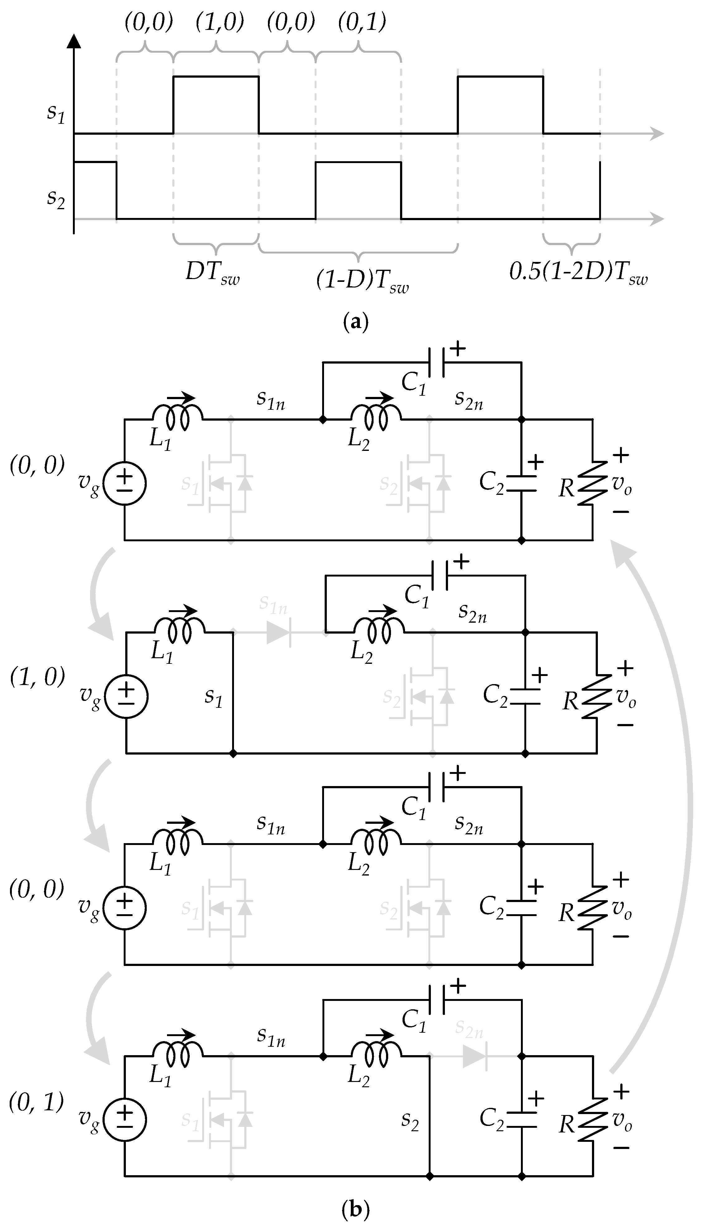
Figure 17a shows the switching signals of the converter when d < 0.5; for example, the duty cycle is 0.3, and the signals are shifted are shifted by half of the switching period (Tsw/2). We can see that, in contrast to the operation when d > 0.5, in this case, the switching state (1, 1) is the one that never appears. Due to the signal’s width, there is a kind of dead-time in which the switching state (0, 0) shows twice in a switching cycle. If we take one switching cycle for analysis, we can see the sequence of switching states is (0, 0), (1, 0), (0, 0), and (0, 1). Figure 17b shows the sequence of switching states, which is useful to understand the average of signals.
Again, we still can use the averaging technique, but in this case, we must observe that the switching period is not split into two different times like in the previous strategy, and in the traditional averaging technique, in which the switching period is divided into the active state dTsw, and the complementary state (1−d)Tsw.
In this case, the switching period is divided into four sub-periods, as shown in Figure 17, the first switching state (0, 0) remains a time 0.5(12d)Tsw, followed by the state (1, 0), which remains for a time dTsw, the third time corresponds again to the state (0, 0), and remains again a time 0.5(12d)Tsw, and the last switching state (0, 1), remains also a time dTsw (see Figure 17a).
The average voltage across inductors L1 and L2, and the average current through capacitors C1 and C2, would be as shown in Equations (31)–(34).
L 1 d i L 1 d t = 0.5 1 2 d v g + v C 1 v C 2 + d v g + 0.5 1 2 d v g + v C 1 v C 2 + d v g + v C 1 v C 2 .
L 2 d i L 2 d t = 0.5 1 2 d v C 1 + d v C 1 + 0.5 1 2 d v C 1 + d v C 2 v C 1 .
C 1 d v C 1 d t = 0.5 1 2 d i L 2 i L 1 + d i L 2 + 0.5 1 2 d i L 2 i L 1 + d i L 2 i L 1 .
C 2 d v C 2 d t = 0.5 1 2 d i L 1 i o + d i o + 0.5 1 2 d i L 1 i o + d i L 1 i L 2 i o .
The set of Equations (31)–(34) may be algebraically simplified as Equations (35)–(38):
L 1 d i L 1 d t = v g + 1 d v C 1 v C 2 .
L 2 d i L 2 d t = d v C 2 v C 1 .
C 1 d v C 1 d t = i L 2 1 d i L 1 .
C 2 d v C 2 d t = 1 d i L 1 d i L 2 i o .
The set of Equations (35)–(38) represents the dynamic model of the converter with the proposed switching scheme when d < 0.5. This model can be used to obtain the steady-state operation. And again, the model is identical to the one derived for the original synchronized strategy, as presented in Equations (5)–(8). This indicates that the proposed operating scheme does not alter the fundamental dynamics nor the steady-state behavior of the converter when the duty cycle exceeds 0.5 or when the duty cycle is lower than 0.5. Equations (9)–(12), which are the steady state, are also valid for this strategy.
Consequently, the intrinsic characteristics of the QBC-NSET, including its voltage conversion ratio and equilibrium operating point, are preserved under the new switching strategy in this operating region. Let us now analyze the switching ripple in passive components.
We can mention that the first three elements (L1, L2, and C1) have the same switching ripple as in the former synchronized switching strategy; only the capacitor C2 has a different (lower) switching ripple. Now, let us explain the switching ripple in this strategy and operation region.
The inductor L1. The switching ripple in the inductor L1 remains the same as in the previous strategy. It can be observed from Figure 12 (former strategy) that L1 gets charged when it is connected to vg during a time dTsw. In Figure 17, during the state (1, 0), the inductor L1 is charged (only in this switching state, L1 gets charged) when connected to the input source vg; this state lasts a time period of dTsw. Then, if we consider that we are not changing the inductance, the switching ripple calculation remains the same as in the previous strategy.
The inductor L2. The switching ripple in the inductor L2 also remains the same as in the previous strategy. It can be observed from Figure 12 (former strategy) that L2 gets charged when the transistors are on, connected to vC2-vC1 during a time dTsw. In Figure 17, during the state (0, 1), the inductor L2 is charged when connected to vC2-vC1. This state lasts a time period of dTsw. Then, if we consider that we are not changing the inductance, the switching ripple calculation remains the same as in the previous strategy.
The capacitor C1. The switching ripple in the capacitor C1 also remains the same as in the previous strategy. It can be observed from Figure 12 (former strategy) that C1 gets charged when the transistors are on, through the current iL2 during a time dTsw. In Figure 17, during the states (1, 0), the capacitor C1 is charged through iL2. This state lasts a time period of dTsw. Then, if we consider that we are not changing the capacitance, the switching ripple calculation remains the same as in the previous strategy.
The capacitor C2. The switching ripple in the capacitor C2 is not the same as in the previous strategy; it is smaller. First of all, let us observe from Figure 12 (former strategy) that C2 gets charged when the transistors are off, through the current iL1-io during a time (1−d)Tsw. When this happens in Figure 12b, the capacitor C1 and the inductor L2 are in a super-node. That is why the capacitor C2 gets charged with the current iL1-io.
In Figure 17, the capacitor C2 is charged in three different periods, two of them have the same switching state (0, 0) with charging current iL1-io, in the other charging state (0, 1), the charging current is iL1-iL2-io. Notice that the switching states in which the capacitor gets charged are ((0, 0)(0, 1)(0, 0)), but we must consider the first (0, 0) is the third appearing in the Figure 17b, and continue until the bottom with the state (0, 1), and consider the top one (0, 0). Those states have a duration equal to (1−d)Tsw since 0.5(12d)Tsw + dTsw + 0.5(12d)Tsw = (1−d)Tsw).
The charging time has a length of (1−d)Tsw, two of the states have the same current as in the former strategy, but the third has a reduced current (iL1-iL2-io), and this reduced current produces a total rise in the ripple that is smaller than in the previous strategy.
As a summary, similar to Equations (13)–(16), the switching ripple in the passive components can be expressed as Equations (26)–(29):
Δ i L 1 = D V g 2 L 1 f s ω .
Δ i L 2 = D 2 L 2 f s ω V C 2 V C 1 = V g 2 L 2 f s ω D 1 D .
Δ v C 1 = D 2 C 1 f s ω I L 2 = I o 2 C 1 f s ω D 1 D .
Δ v C 2 = 1 2 C 2 f s ω 0.5 1 2 D I L 1 I o + D I L 1 I L 2 I o + 0.5 1 2 D I L 1 I o
Δ v C 2 = 1 2 C 2 f s ω 1 D I L 1 I o D I L 2 .
The voltage ripple expressed in Equation (43) is smaller than the one expressed in Equation (16), by the factor -DiL2; the reduction can also be verified by simulation. The output voltage ripple of the converter in this operating region with the proposed strategy is given by Equation (43), which can be simplified as Equation (44).
Δ v o = Δ v C 2 = I o 2 C 2 f s ω D 1 D 1 D .
This case can be a particular case of any of the previous two operating conditions; still, we will explain it. We can close the section, concluding that the output voltage ripple is expected to be smaller than in the previous operation.
Recalling the voltage ripple in C2, which is the output voltage ripple. In this operation, the charging of the capacitor is made in three different consecutive states (0, 0), (0, 1), and (0, 0). The fact that it is getting charged in three different states does not mean it receives more charge than in the previous operation, but the calculation involves those three states.
During the state (0, 0), which is also depicted in Figure 13, the capacitor gets IL1-Io, during the state (0, 1), which is also depicted in Figure 16, the capacitor gets IL1-IL2-Io, and finally, during the last state (0, 0), the capacitor gets again IL1-Io. Those currents are indicated in (42) as well as the time each state remains. Finally (44) is an algebraic simplification of (42).
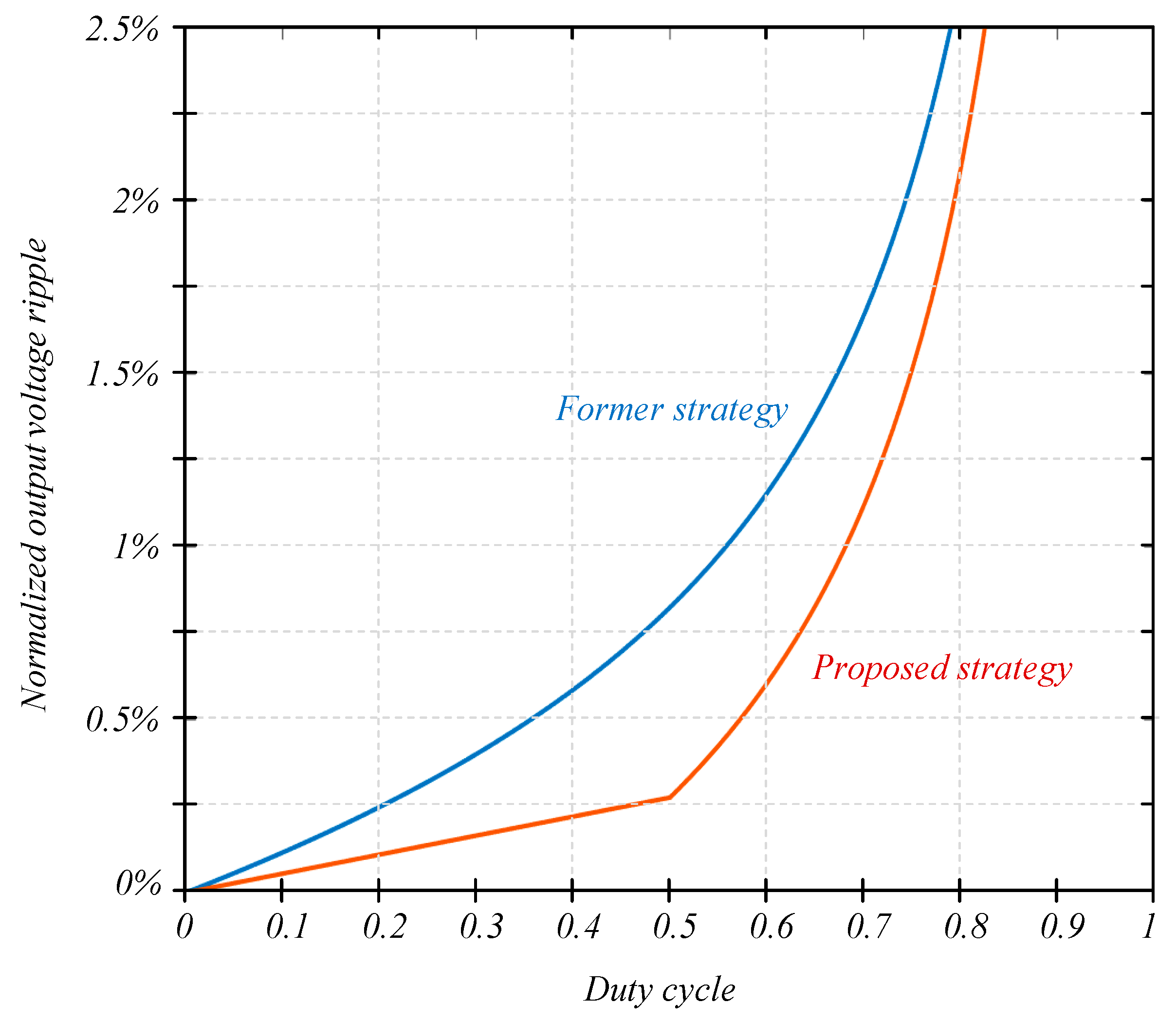
To provide a clearer quantitative evaluation of the ripple reduction achieved with the proposed switching strategy, the output voltage ripple was calculated in normalized form with respect to the average output voltage for both the former and the proposed strategy. The normalized ripple is defined as the ratio between the ripple amplitude and the average output voltage, expressed as a percentage.
The normalized voltage ripple in percentage, for the former strategy, can be written as Equation (45).
Δ v o 1 n = 100 2 C 2 R f s ω 1 ( 1 D ) 2 1 D = β 1 ( 1 D ) 2 1 D .
Similarly, the normalized voltage ripple in percentage, for the proposed strategy when D < 0.5, can be written as Equation (46).
Δ v o 2 n = 100 2 C 2 R f s ω D 1 D 1 D = β D 1 D 1 D .
And the normalized voltage ripple in percentage, for the proposed strategy when D > 0.5, can be written as Equation (47).
Δ v o 3 n = 100 2 C 2 R f s ω D ( 1 D ) 2 1 D = β D ( 1 D ) 2 1 D .
Let us consider numerical values like the one used in the experimental section, in which C2 = 6.8 µF, fsw = 100 kHz, R = 133.33 Ω, which is the equivalent resistance of a 300 W load with 200 V at the output. This would lead to a β = 0.55 in (45)–(47).
Figure 18 shows the normalized output voltage ripple obtained for both the former switching strategy and the proposed switching strategy. The comparison highlights the reduction achieved with the proposed approach across the evaluated operating conditions. Table 1 also shows the comparison in a numerical manner.

3.3. Comments Related to the Voltage and Current Stress in Components

At this point, it is useful to highlight the impact of the proposed switching strategy on the current and voltage stresses of the converter components. From the analysis presented for both the original synchronized operation and the proposed switching strategy so far, it can be observed that the voltage and current stresses across most components remain unchanged. For example, from the equivalent circuits, we can see the inductors charge and discharge with the same amount of voltage, and they drain the same DC current (same DC current and same current ripple). Something similar happens to the capacitor C1 and the semiconductor devices; they experience the same operating conditions as in the original switching scheme, since the duty cycle and the fundamental steady-state relationships of the converter are preserved.
The only component whose operating conditions are modified is the output capacitor C2. Under the proposed switching strategy, although the DC voltage remains unchanged, the charging current of C2 changes from iL1−io (in the former synchronized operation) to iL1−iL2−io during the relevant switching interval. As a consequence, the current stress on the output capacitor is reduced. This reduction in capacitor current directly explains the decrease in the output voltage ripple obtained with the proposed switching strategy.
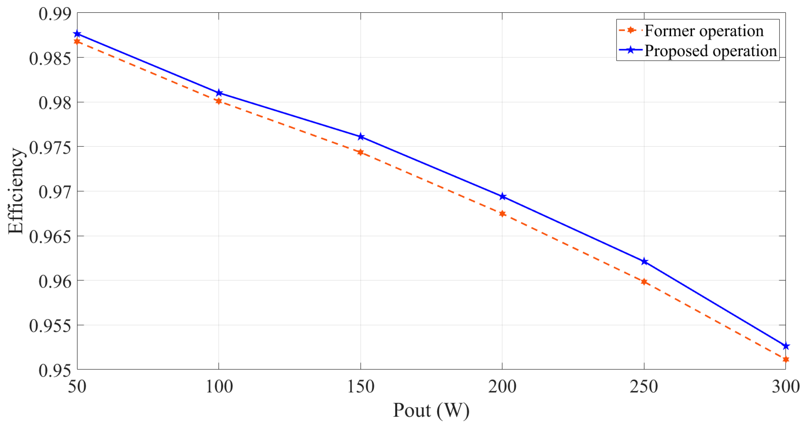
Although power losses in capacitors are usually small, since their equivalent series resistance is given in milli-Ohms, this reduction in the current stress leads to a slightly larger efficiency.

3.4. Critical Inductor Values for Ensuring Continuous Conduction Mode (CCM)

We can calculate the critical inductances L1crit and L2crit; these are the minimum inductance values to ensure the inductors will operate in continuous conduction mode (CCM). We can do that by equating the inductor’s current ripple (26) or (39) and (27) or (40) with their DC current (11) and (12).
I o 1 D 2 = D V g 2 L 1 c r i t f s ω .
L 1 c r i t = D V g 1 D 2 I o 2 f s ω .
I o 1 D = V g 2 L 2 c r i t f s ω D 1 D .
L 2 c r i t = V g D I o 2 f s ω .
Considering the output current Io can be written as (52).
I o = V g 1 D 2 R .
R is the load resistance. The critical inductance values can be written as:
L 1 c r i t = R D 1 D 4 2 f s ω .
L 2 c r i t = R D 1 D 2 2 f s ω .
For ensuring operation in continuous conduction mode, the inductance value of L1 must be equal to or larger than L1crit, and the inductance value of L2 must be equal to or larger than L2crit.

3.5. Design Methodology

The following procedure summarizes the main steps required to design the proposed QBC-NSET converter based on the specifications used in the experimental prototype.
Step 1. Define specifications. The design begins with the initial electrical specifications of the converter. There are specifications that may be given in a range, like the input voltage Vg, the output voltage Vo, and the output power Po. The calculations are usually made in one of the extreme conditions, like maximum output power or maximum voltage gain. The switching frequency fsw is usually also provided as a fixed design specification; the input current ripple Δig and output voltage ripple Δvo are provided as a minimum value specification.
In this step, we can calculate the voltage gain M = Vo/Vg, and the duty cycle from the gain Equation (55).
M = 1 1 D 2 .
Step 2. Component selection. The capacitors can be chosen according to their ripple equations. The design begins with the initial electrical specifications of Equations (26)–(29). In the case of the inductors, their inductance must be equal to or greater than the ones obtained from Equations (26) and (27), but also they must be larger than their critical values provided in Equations (53) and (54). The switches and diodes must be selected according to the maximum voltage stress derived in the steady-state analysis. Current ratings must also exceed the maximum inductor currents with an appropriate safety margin.
Step 3. The design must be verified through simulation and experimental validation. The parameters selected using the previous procedure were used to construct the experimental prototype.
Step 4. Finally, according to the applications, a control strategy may be defined, and a controller may be implemented and tested.

4. Experimental Results

To validate the theoretical developments and verify the effectiveness of the proposed switching strategy, an experimental prototype of the Quadratic Boost Converter based on Non-Series Energy Transfer (QBC-NSET) was designed and constructed. The prototype was evaluated under identical operating conditions using both the original synchronized switching scheme and the proposed phase-shifted switching strategy.
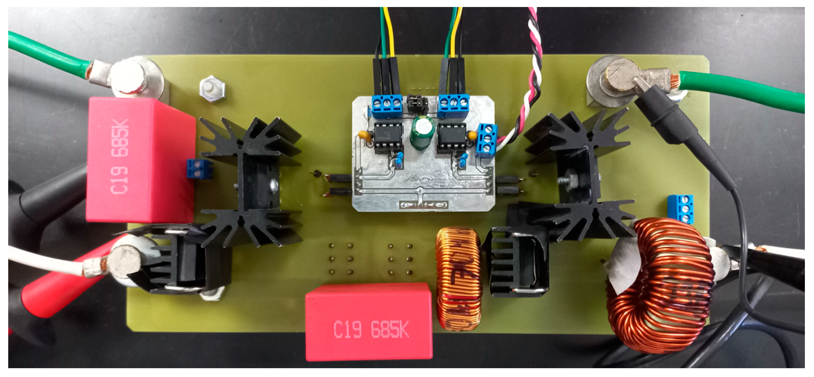
Figure 19 shows the photo of the experimental prototype, and Table 2 shows the parameters used in the design.
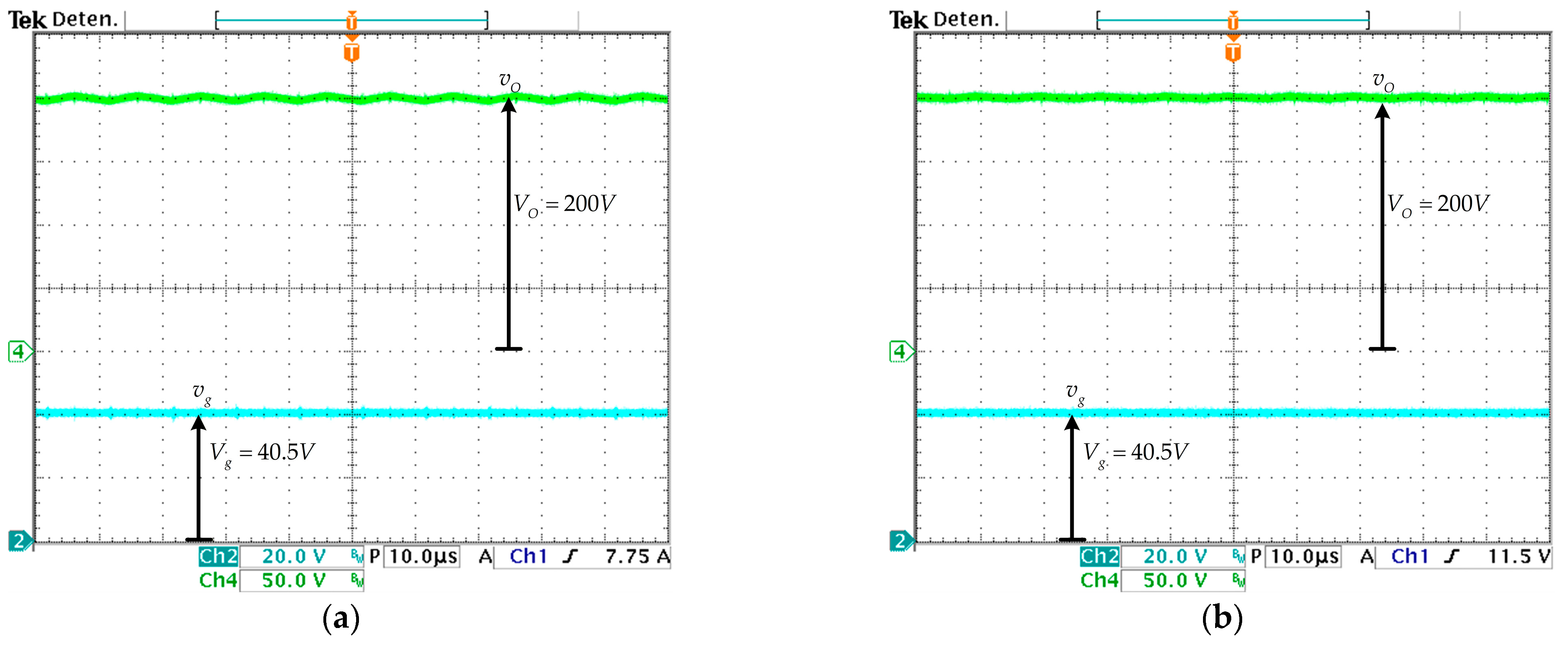
Several tests were performed, including with duty cycles equal, under, and over 0.5. Figure 20 shows the static gain with an output voltage of 200 V and a duty cycle of 0.45, with the former and with the proposed switching strategy.
In both cases, the input voltage is shown in blue with 20 V/div and 10μS/div, while the output voltage is shown in green with 50 V/div and 10μS/div. It is possible to observe that the switching ripple is smaller in the proposed operation.
To better appreciate the output voltage ripple, a zoom-in on the voltages is shown in Figure 21.
Figure 21a shows a zoom of the output voltage with the previous switching strategy, at 2.5 V/div and 4 μS/div, while Figure 21b shows a zoom of the output voltage with the proposed operation, also at 2.5 V/div and 4 μS/div.
In this particular operating condition, the proposed strategy has 40% (1.2/3) of the output voltage ripple compared to the former strategy, a reduction of 60%.
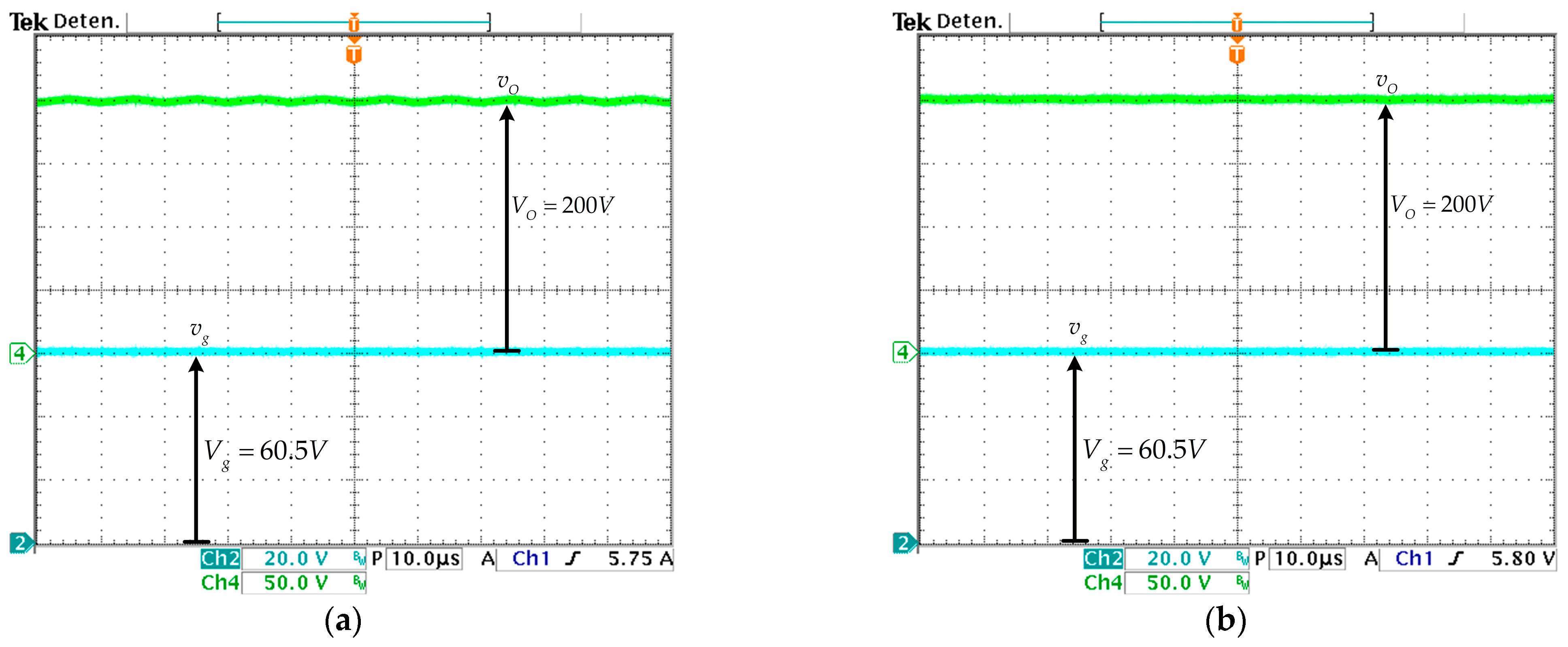
Figure 22 shows the static gain with an output voltage of 200 V and a duty cycle of 0.5, with the former and with the proposed switching strategy. In both cases, the input voltage is shown in blue with 20 V/div and 10 μS/div, while the output voltage is shown in green with 50 V/div and 10 μS/div.
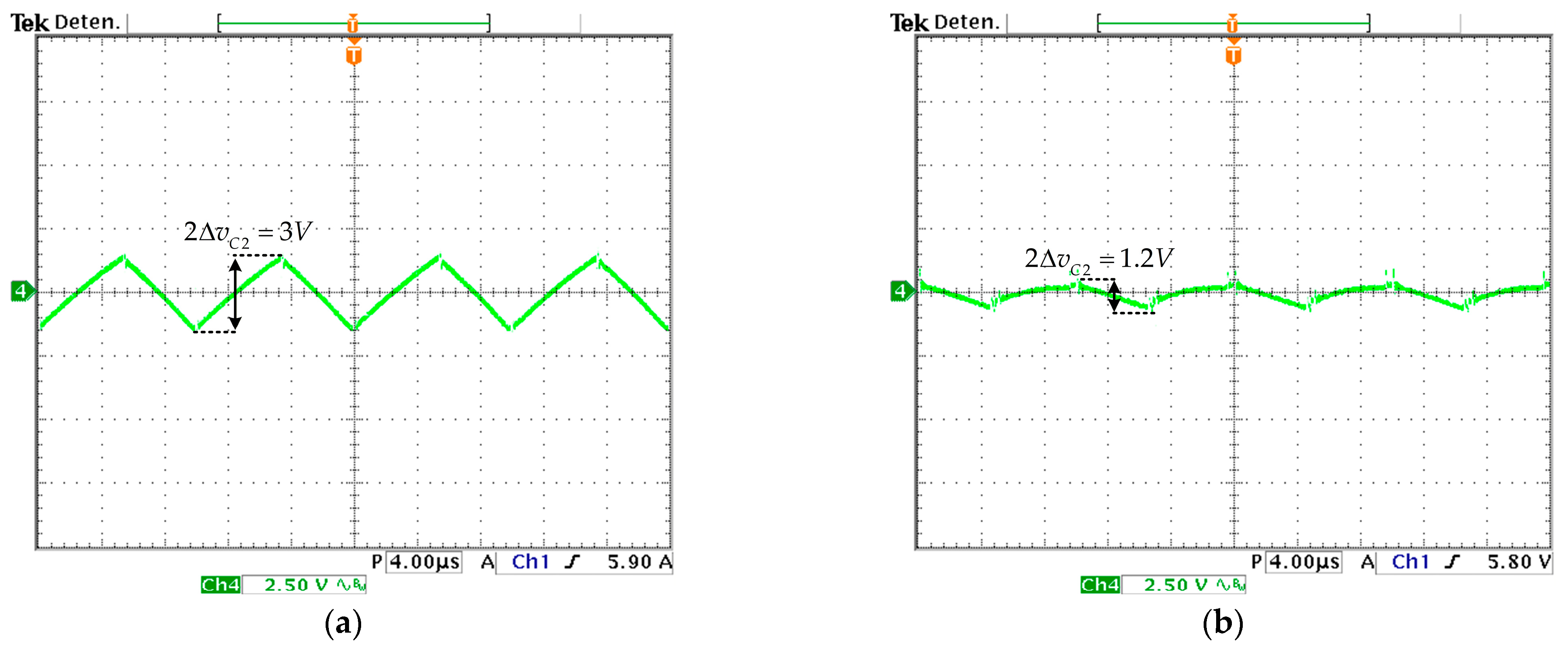
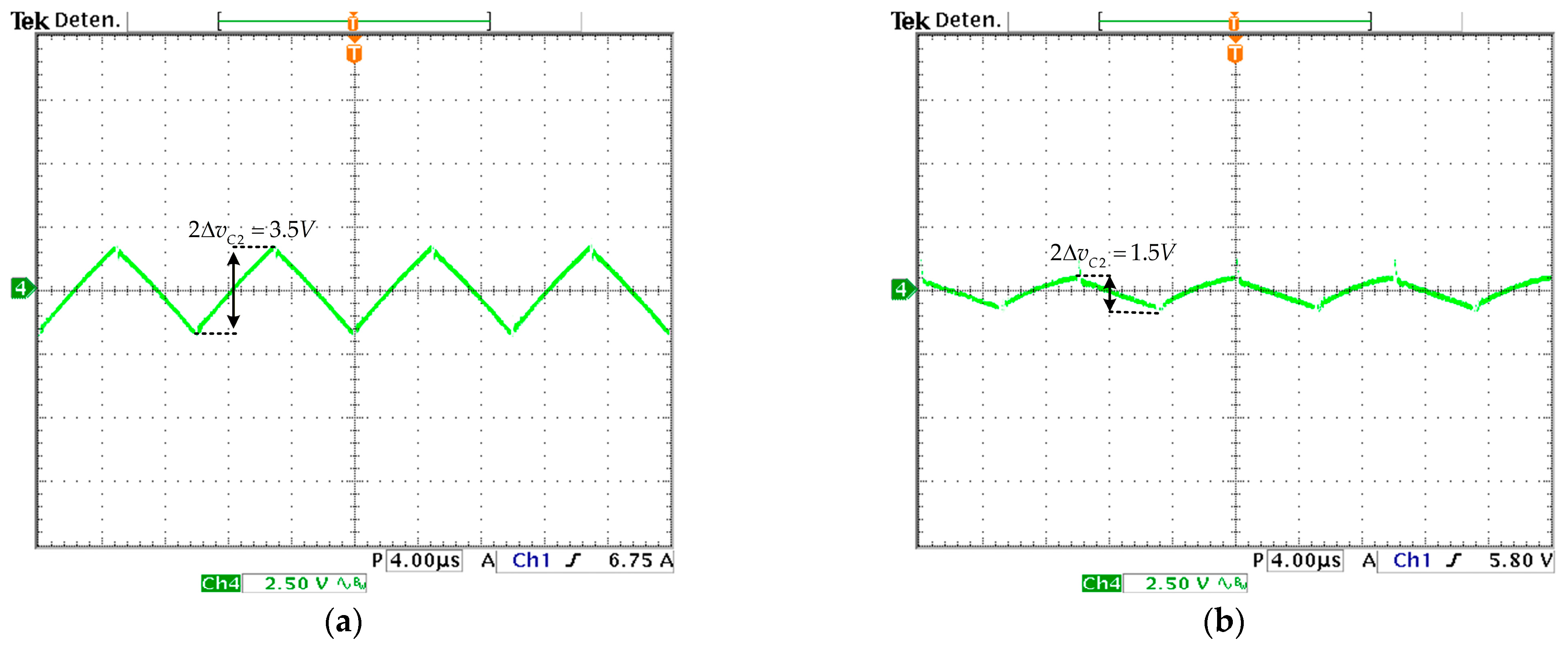
Similarly to Figure 21. To better appreciate the output voltage ripple, a zoom-in on the voltages is shown in Figure 23. Figure 23a shows a zoom of the output voltage with the previous switching strategy, at 2.5 V/div and 4 μS/div, while Figure 23b shows a zoom of the output voltage with the proposed operation, also at 2.5 V/div and 4 μS/div.
In this particular operating condition (D = 0.5), the proposed strategy has 42.8% (1.5/3.5) of the output voltage ripple compared to the former strategy, a reduction of 57.14%.
Figure 24 shows the static gain with an output voltage of 200 V and a duty cycle of 0.55, with the former and with the proposed switching strategy. In both cases, the input voltage is shown in blue with 20 V/div and 10 μS/div, while the output voltage is shown in green with 50 V/div and 10 μS/div.
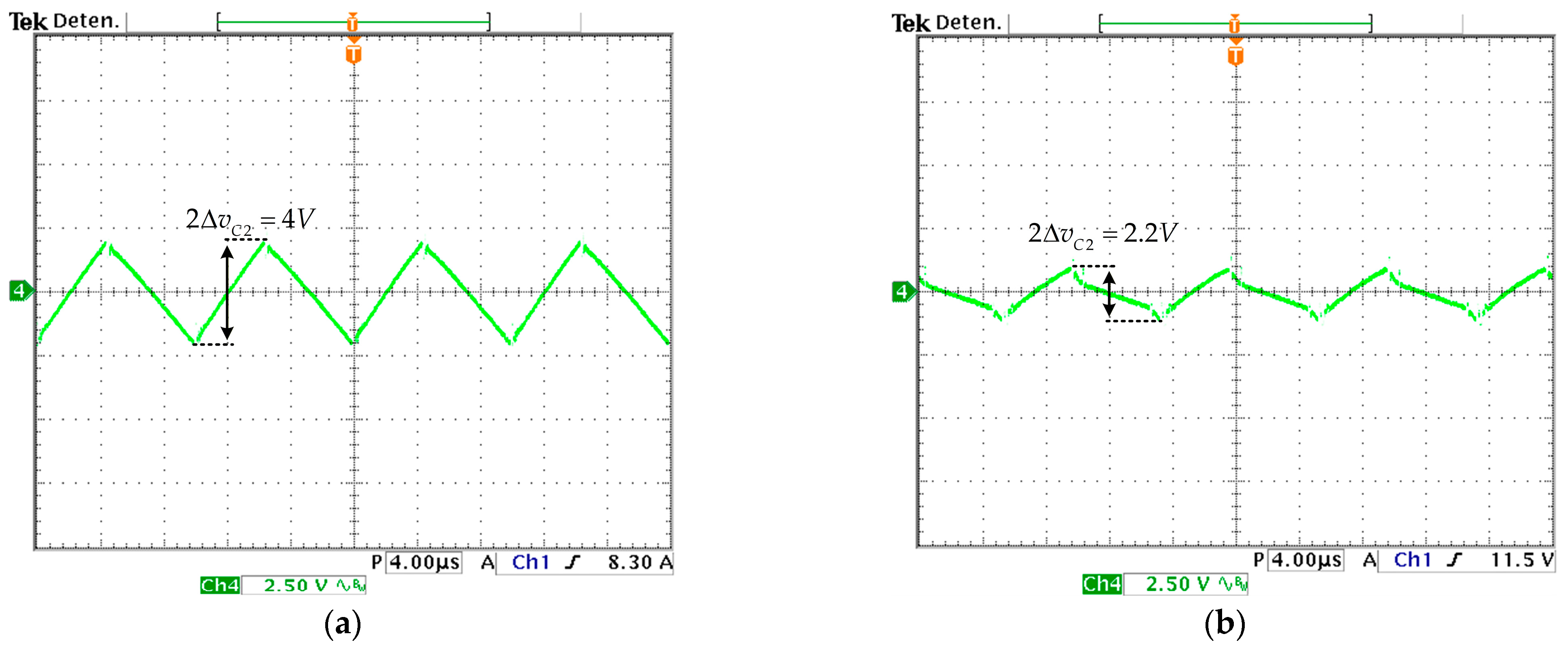
A zoom-in on the voltages is shown in Figure 25. Figure 25a shows a zoom of the output voltage with the previous switching strategy, at 2.5 V/div and 4 μS/div, while Figure 25b shows a zoom of the output voltage with the proposed operation, also at 2.5 V/div and 4 μS/div.
In this particular operating condition (D = 0.55), the proposed strategy has 55% (2.2/4) of the output voltage ripple compared to the former strategy, a reduction of 65%.
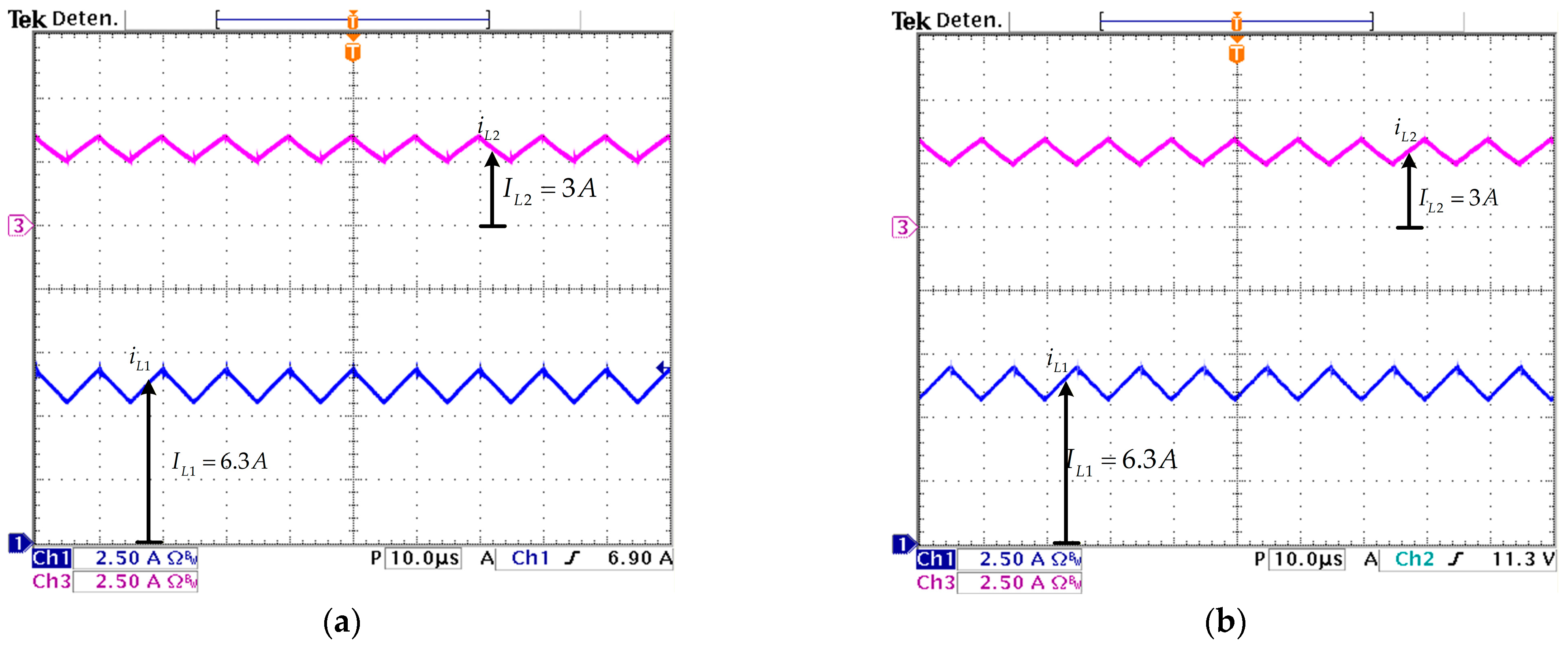
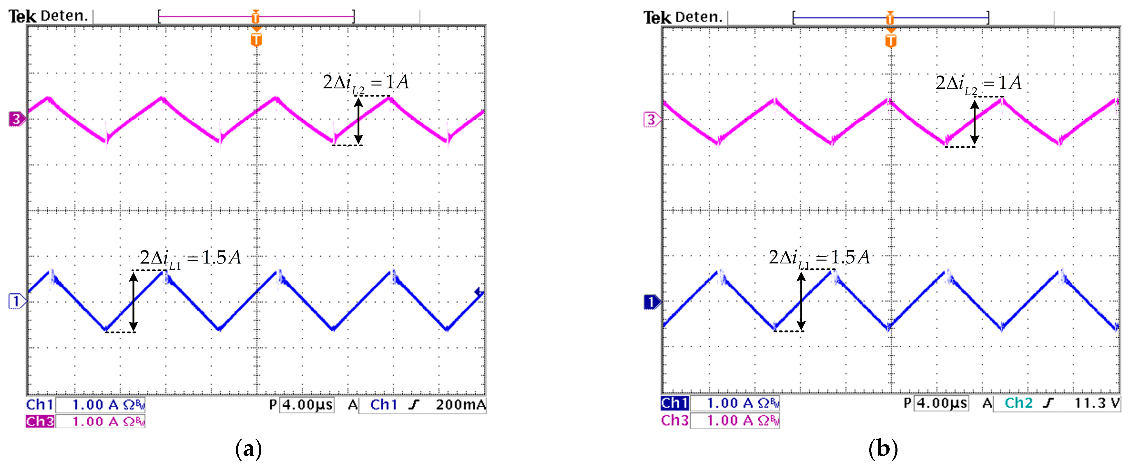
Other important waveforms for both the former and the proposed switching strategies were captured for D = 0.5. Figure 26 shows the current through the inductors, with the former (Figure 26a) and with the proposed (Figure 26b) switching strategy. In both cases, the inductor currents are shown with 2.5 A/div and 10 μS/div.
A zoom-in on the inductor currents (with ac coupling) is shown in Figure 27. Figure 27a shows the zoom of the inductors’ current with the previous switching strategy, at 1 A/div and 4 μS/div, while Figure 27b shows the zoom of the inductors’ currents with the proposed operation, also at 1 A/div and 4 μS/div. The ripples are equal in both strategies since the duty cycle of the driving transistors does not change.
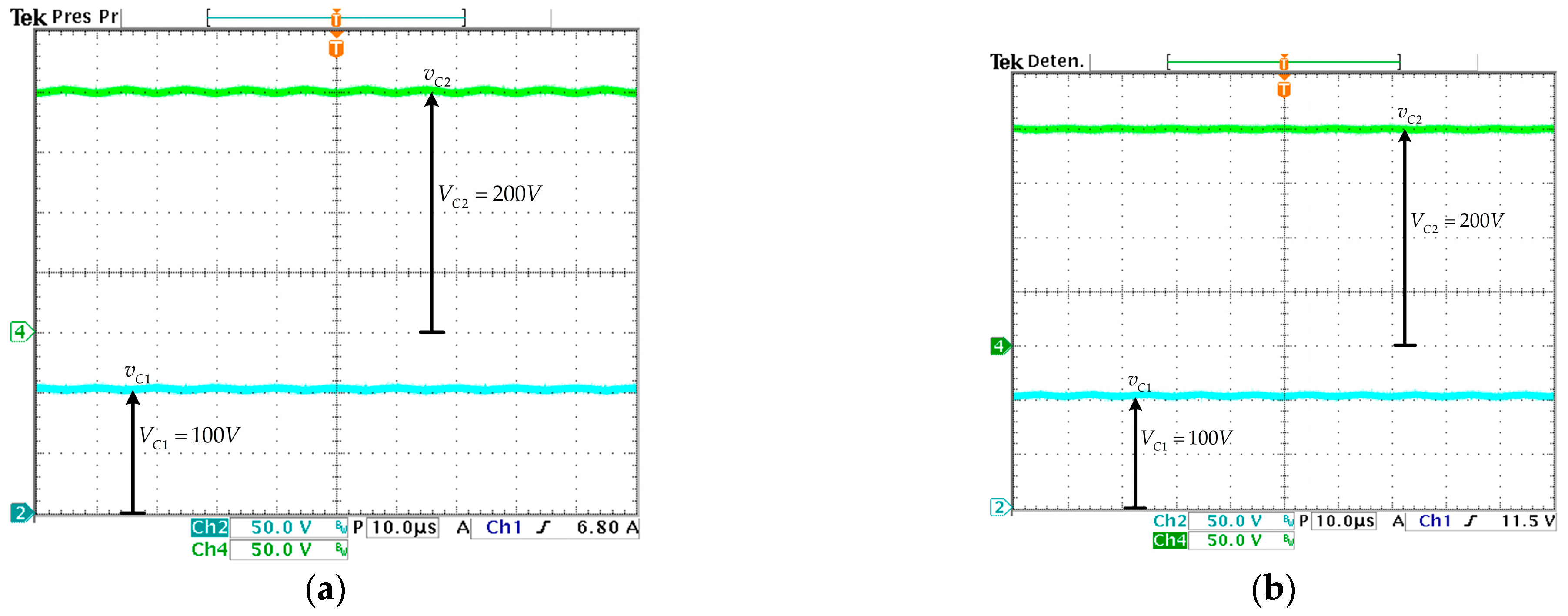
Figure 28 shows the voltage across capacitors for D = 0.5, with the former (Figure 28a) and with the proposed (Figure 28b) switching strategy. In both cases, the voltages are shown with 50 V/div and 10 μS/div.
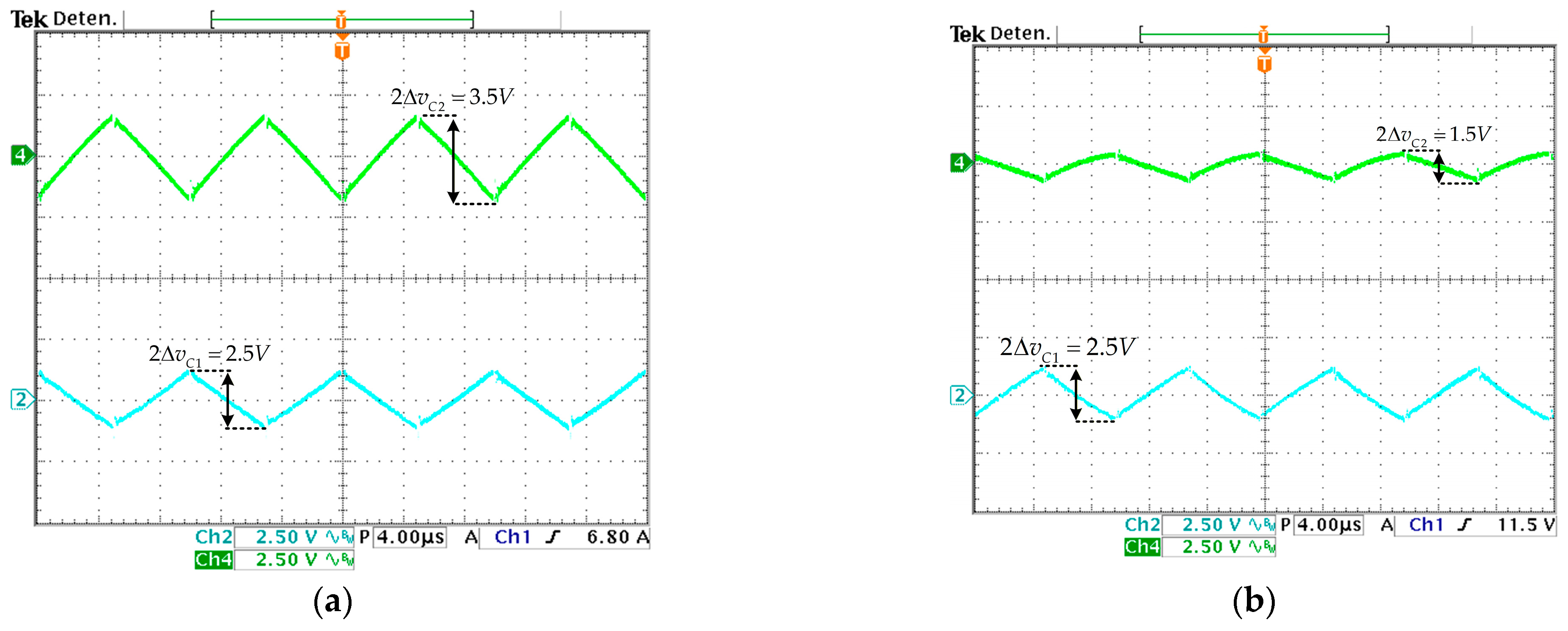
A zoom-in on the capacitors’ voltage (with AC coupling) is shown in Figure 29. Figure 29a shows the zoom of the capacitors’ voltage with the previous switching strategy, at 2.5 V/div and 4 μS/div, while Figure 29b shows the zoom of the capacitors’ voltage with the proposed operation, also at 2.5 V/div and 4 μS/div.
We can see that the advantage of the proposed strategy is reducing the voltage ripple in the output capacitor.
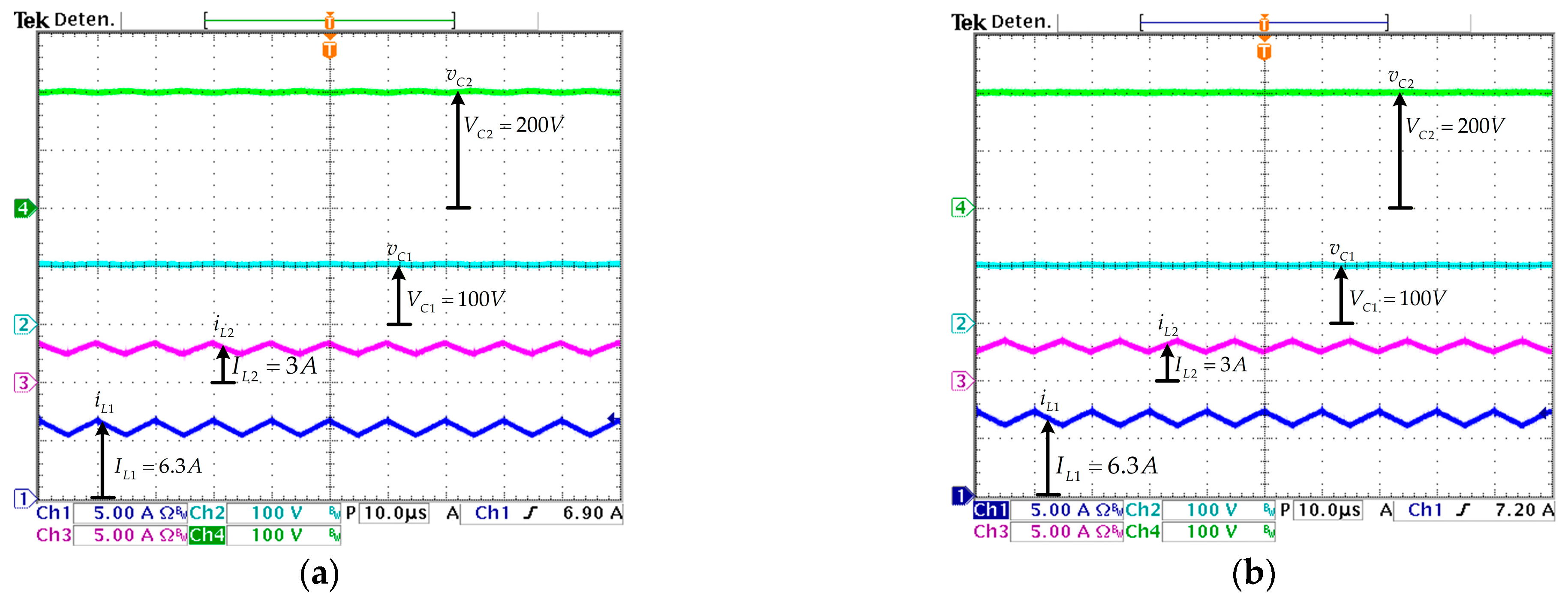
As a summary, Figure 30 shows the fourth state variables of the converter in this operating condition (D = 0.5), the voltage across capacitors for D = 0.5, with the former (Figure 28a) and with the proposed (Figure 28b) switching strategy. In both cases, the voltages are shown with 50 V/div and 10 μS/div.
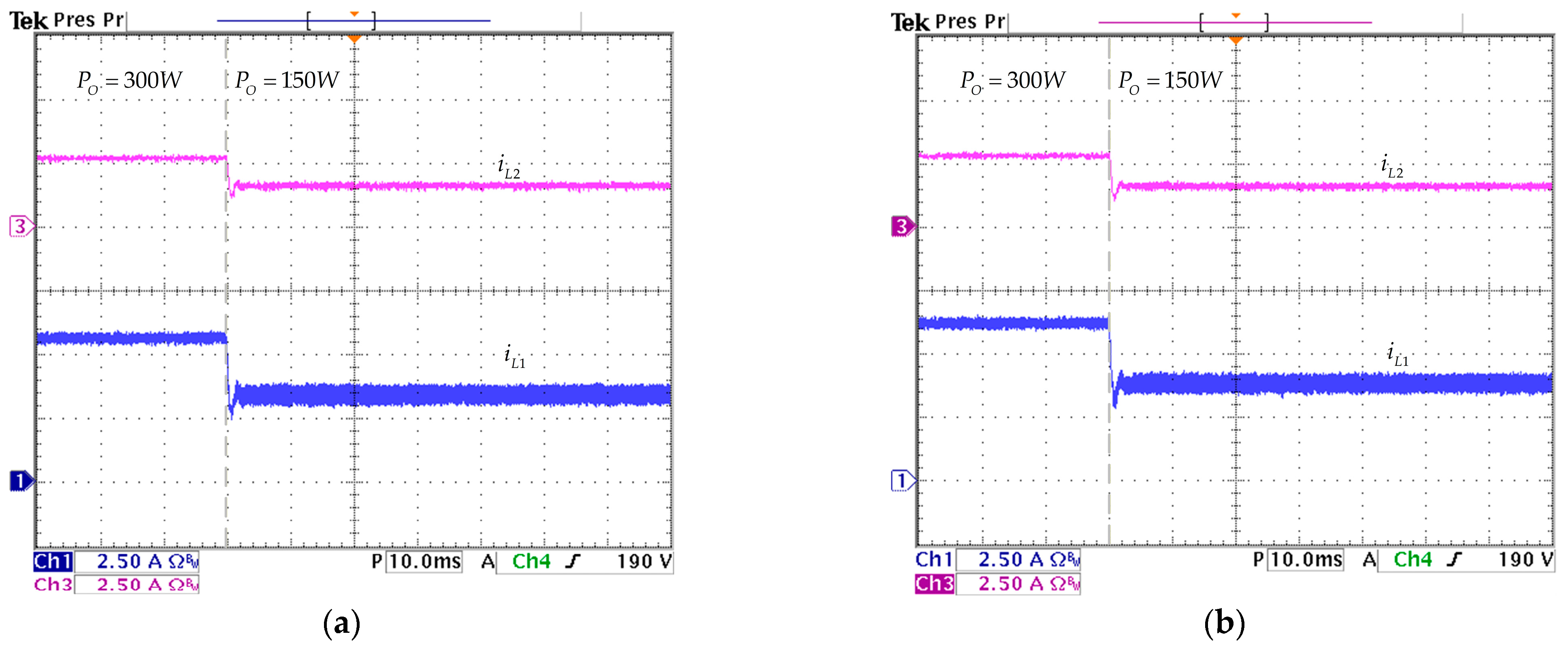
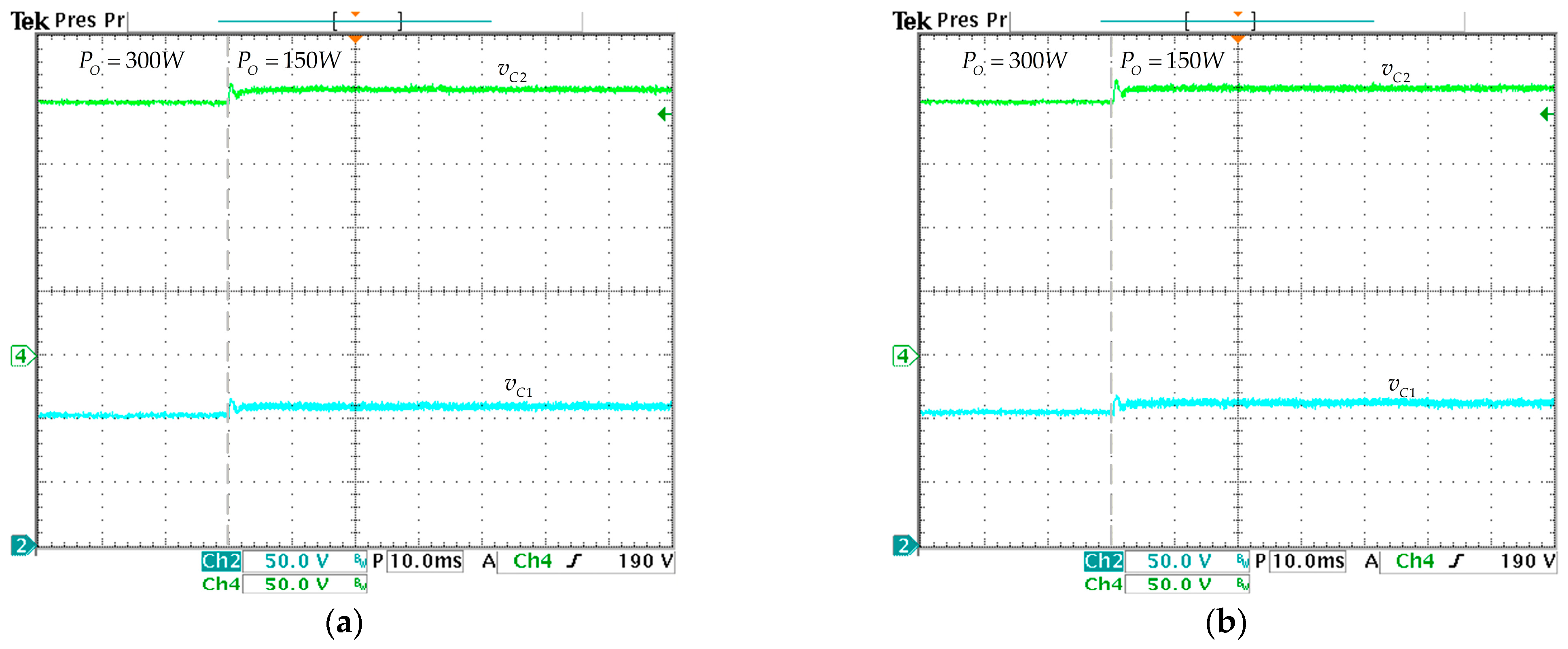
Theoretically, the proposed switching strategy does not alter the dynamic model, and then the dynamic behavior of the converter; the dynamic model is the same in both operating conditions. To better appreciate this, we performed a dynamic test of power change in which the converter was operating at 300 W, and the output power suddenly changed to 150 W. The converter was operated in open loop to better appreciate the behavior of its dynamical model without being modified by a controller. The converter behaves similarly under those tests. Figure 31 shows the inductor currents for this test, and Figure 32 shows the capacitors’ voltages.
Finally, Figure 33 shows the experimentally measured efficiency of the converter with both the former and the proposed switching strategy.

4.1. Quantitative Comparison

This subsection presents a comparison of output voltage ripple with the following converters: (i) The cascaded connection of two conventional boost converters. (ii) The traditional quadratic boost converter (single-switch structure). (iii) The original QBC-NSET operating under synchronized switching. Those topologies were chosen since they provide the same voltage gain, and they all have continuous input current characteristics due to the existence of an input inductor.
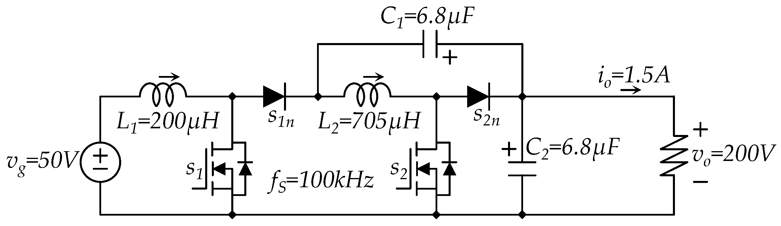
Converters are shown with the parameters used in the experiments of the article. Figure 34 shows the QBC-NSET, their output voltage ripple with the former switching strategy can be calculated with Equation (17), solved here as Equation (56).
Δ v o = 1.5 2 × 6.8 μ × 100 k 1 ( 1 0.5 ) 2 1 0.5 = 1.65 .
With the proposed switching strategy, their output voltage can be calculated with converters are shown with the parameters used in the experiments of the article. Figure 34 shows the QBC-NSET, their output voltage ripple with the former switching strategy can be calculated with Equation (17), solved here as Equation (57).
Δ v o = 1.5 2 × 6.8 μ × 100 k 0.5 ( 1 0.5 ) 2 1 0.5 = 0.55 .
Figure 35 shows the cascaded boost converter, while Figure 36 shows the single-switch traditional quadratic boost converter; in both cases, the output voltage ripple can be calculated with Equations (58) and (59).
Δ v o = I o D 2 C 2 f s ω .
Δ v o = 1.5 × 0.5 2 × 6.8 μ × 100 k = 0.55
At the selected operating point and using the same parameters for the passive components and switching frequency, the output voltage ripple of the QBC-NSET under the proposed switching strategy is equivalent to that of the traditional quadratic boost converter and the cascaded boost configuration.
Unlike the cascaded boost converter, the QBC-NSET maintains its intrinsic non-series energy-transfer characteristic, reducing redundant energy processing between stages. Moreover, in comparison with the original synchronized operation of the QBC-NSET, the proposed switching strategy effectively reduces the output voltage ripple and brings it to the same level as the traditional quadratic boost converter, without increasing switching frequency or stored energy in the passive components.
Consequently, the proposed operation maintains the structural and energy-processing advantages of the QBC-NSET while improving its output voltage ripple performance relative to its previous operating mode.

4.2. Transient Dynamic Response Under Former and Proposed Switching Strategies

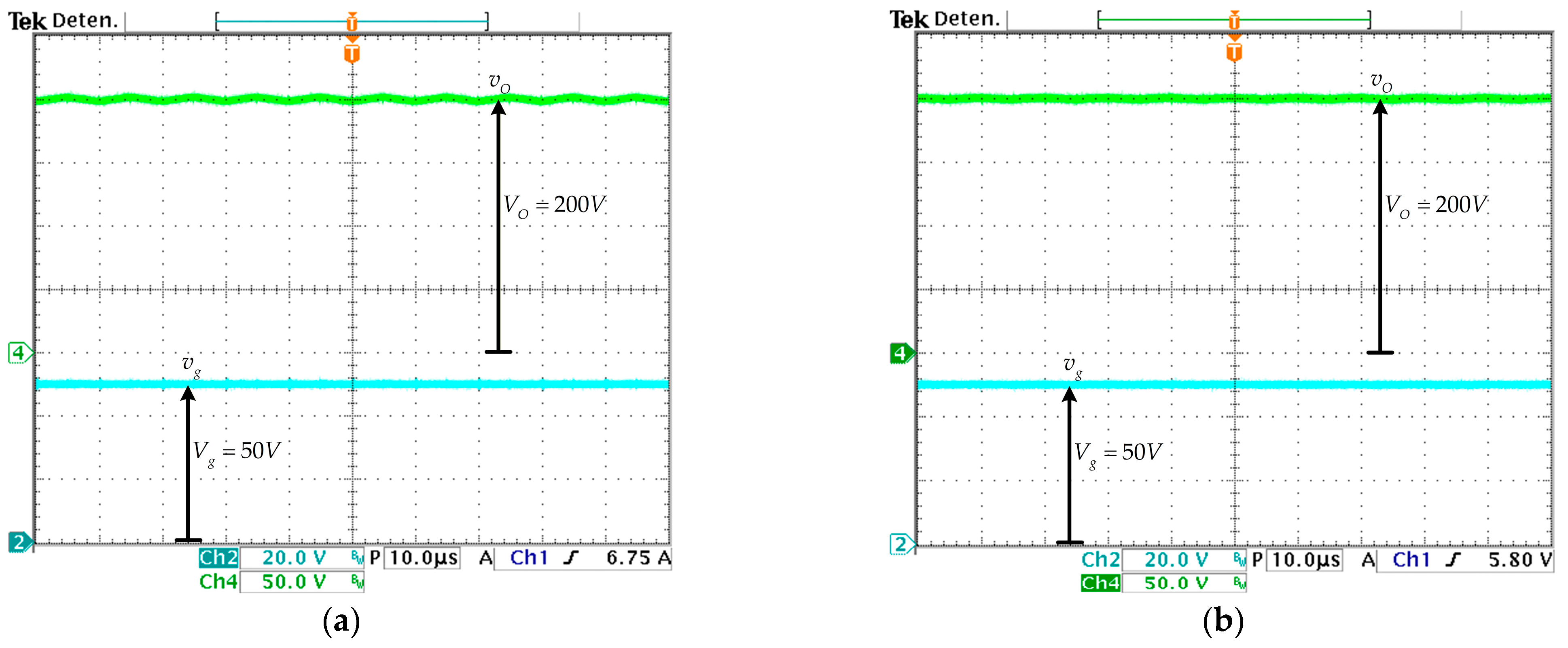
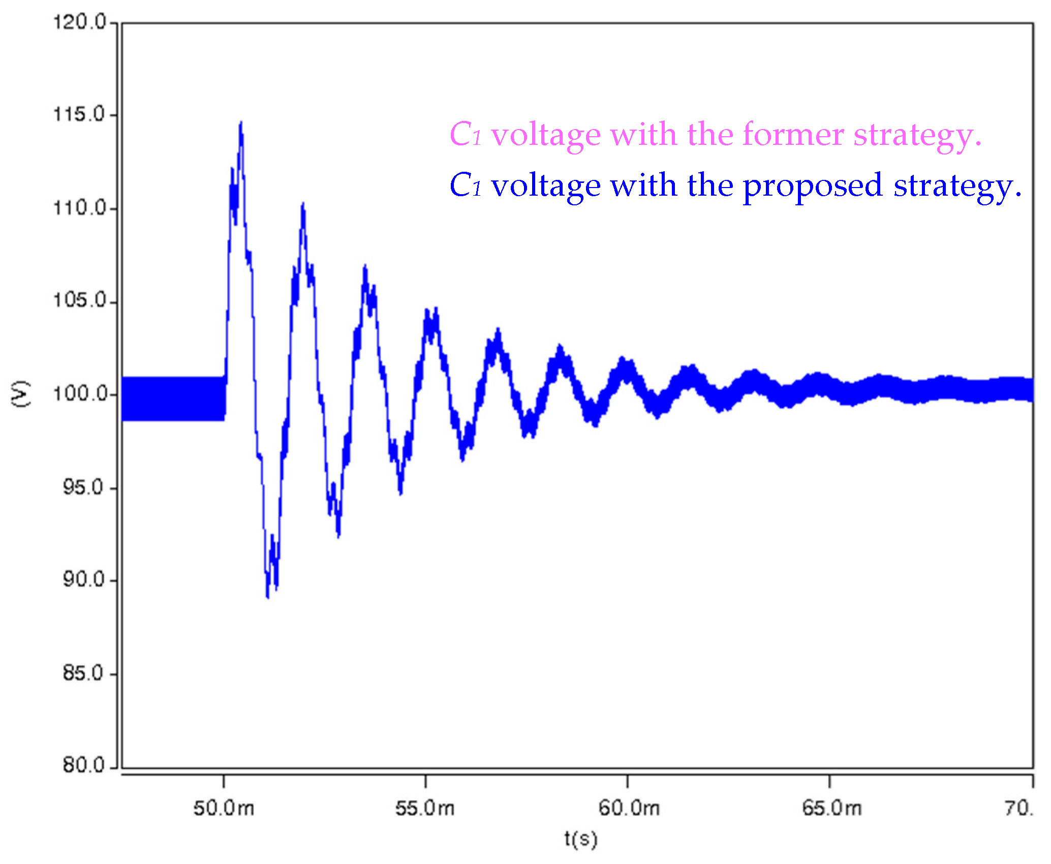
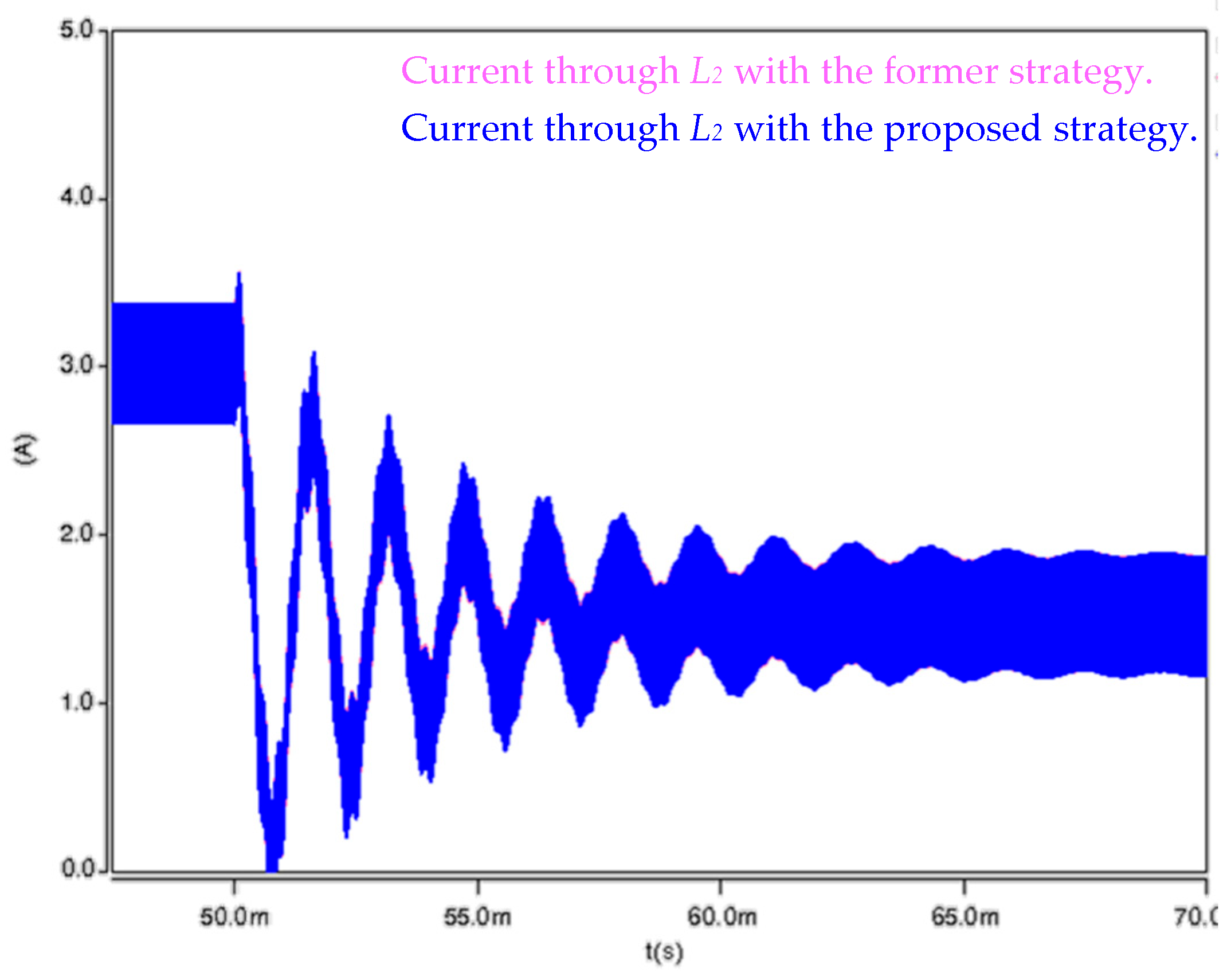
In this section, a transient dynamic response is presented in simulation in order to verify that the averaged dynamic model of the converter is not affected by the modification of the switching strategy. The parameters used in the simulation are also the ones shown in Table 2. The test corresponds to a load rejection condition, in which the converter is working in steady state, with 50 V input, 200 V output, and 300 W of load power. Then the output power is suddenly reduced from 300 W to 150 W.
In the presented waveforms, the light-pink traces represent the converter response under the former switching strategy, whereas the dark-blue traces correspond to the proposed switching scheme. It can be observed that the light-blue signal in Figure 37 appears thicker due to the higher switching ripple; however, its average values closely follow those obtained with the proposed strategy. This result confirms that the transient dynamic behavior of the converter remains essentially unchanged, which is consistent with the theoretical prediction that the averaged dynamic model is not modified by the new switching approach. Figure 37 shows the output voltage in both the former and the proposed strategy during the load rejection disturbance.
Figure 38 shows the input current in both the former and the proposed strategy.
In this case (see Figure 38), signals have the same waveforms and switching ripple; there is no apparent difference, and small signs of the pink waveforms are shown in some places.
Figure 39 shows the voltage across C1 in both the former and the proposed strategy during the load rejection disturbance. Similarly to Figure 38, there is no difference between bot signals; the pink signal hides perfectly below the blue signal.
Figure 40 shows the current through the inductor L2 in both the former and the proposed strategy during the load rejection disturbance. Similarly to Figure 39, there is no difference between the two signals; they have the same waveform and the same switching ripple; the pink signal hides perfectly below the blue signal.

5. Conclusions

This paper has presented a different switching strategy for a quadratic boost converter based on non-series energy transfer (QBC-NSET), aimed at reducing the output voltage ripple without modifying the converter hardware. Unlike the original synchronized switching scheme, the proposed operation employs independently phased gating signals for the two active switches, allowing additional switching states to appear during a switching period.
A detailed analytical study demonstrated that, for both operating regions d > 0.5 and d < 0.5, the averaged dynamic model obtained under the proposed switching strategy is mathematically identical to that derived for the original synchronized operation. Consequently, the fundamental characteristics of the converter, including its steady-state behavior and quadratic voltage conversion ratio, remain unchanged. This result confirms that the proposed switching approach does not compromise the intrinsic performance of the QBC-NSET.
The analysis of switching ripple revealed that the proposed strategy reduces the output voltage ripple by altering the charging intervals and charging current of the output capacitor C2, while preserving the ripple characteristics of the remaining passive components. Importantly, this improvement is achieved without increasing the switching frequency or requiring larger inductors or capacitors, thus avoiding additional stored energy or increased system cost.
Experimental results obtained from a laboratory prototype validated the analytical findings, confirming a reduction in output voltage ripple compared to the conventional synchronized operation. The proposed switching strategy, therefore, represents an effective and low-complexity solution to enhance the output voltage quality of the QBC-NSET.

Author Contributions

Authors L.H.D.-S. and J.C.R.-C. contributed with the conceptualization of the article, J.L.-R. and J.G.G.-H. contributed to the methodology, F.B.-C. and J.P. contributed with the validation, L.H.D.-S. and J.C.R.-C. contributed with the investigation, J.L.-R. and J.G.G.-H. contributed with the formal analysis, and J.C.R.-C. and L.H.D.-S. wrote the draft and manuscript preparation. All authors have read and agreed to the published version of the manuscript.

Funding

This research received no external funding.

Institutional Review Board Statement

Not applicable.

Informed Consent Statement

Not applicable.

Data Availability Statement

The original contributions presented in this study are included in the article. Further inquiries can be directed to the corresponding authors.

Acknowledgments

The authors would like to thank the Instituto Potosino de Investigación Científica y Tecnológica A.C. (IPICYT), Mexico, Universidad Panamericana (UP), Mexico, Tecnológico Nacional de México/Instituto Tecnológico de Ciudad Madero, Mexico, Universidad Tecnológica de Altamira, Mexico, Universidad Autónoma Metropolitana (UAM), Mexico, and the Universidad Autónoma de Occidente. The authors acknowledge the use of ChatGPT 5.3 (OpenAI, San Francisco, CA, USA) for language translation and minor stylistic refinement of selected explanatory passages from Spanish to English. The tools were not used to generate scientific content, data, figures, study design, analysis, or interpretation. All scientific contributions and conclusions are solely those of the authors.

Conflicts of Interest

The authors declare no conflicts of interest.

References

  1. Lazaroiu, A.C.; Gmal Osman, M.; Strejoiu, C.-V.; Lazaroiu, G. A Comprehensive Overview of Photovoltaic Technologies and Their Efficiency for Climate Neutrality. Sustainability 2023, 15, 16297. [Google Scholar] [CrossRef]
  2. Muhammad, S.; Isa, G.I. Solar photovoltaic technologies: A critical review of technological developments, implementation challenges, and future prospects. Int. J. Manag. Appl. Sci. Res. 2025, 8, 192–223. [Google Scholar] [CrossRef]
  3. Hazim, H.I.; Baharin, K.A.; Gan, C.K.; Sabry, A.H.; Humaidi, A.J. Review on Optimization Techniques of PV/Inverter Ratio for Grid-Tie PV Systems. Appl. Sci. 2023, 13, 3155. [Google Scholar] [CrossRef]
  4. Webb, D.; Kneifel, J.; O’Fallon, C.M. Developing Cost Functions for Estimating Solar Photovoltaic System Installed and Life Cycle Costs Using Historical Quote Data; NIST Technical Note 2113; US Department of Commerce, National Institute of Standards and Technology: Washington, DC, USA, 2020. [Google Scholar]
  5. Araújo, I.; Nunes, L.J.R.; Vilas, D.P.; Curado, A. Integrating Renewable Energy Produced by a Library Building on a University Campus in a Scenario of Collective Self-Consumption. Energies 2024, 17, 3405. [Google Scholar] [CrossRef]
  6. Schetinger, A.M.; Lucena, A.F. Evaluating policy frameworks and their role in the sustainable growth of distributed photovoltaic generation. Resources 2025, 14, 28. [Google Scholar] [CrossRef]
  7. Antunes, F.A.F.; Freitas, J.B.F.; Prado, C.A.; Castro-Alonso, M.J.; Díaz-Ruíz, E.; Mera, A.E.M.; Santos, J.C.; Silva, S.S. Valorization of corn cobs for xylitol and bioethanol production through column reactor process. Energies 2023, 16, 4841. [Google Scholar] [CrossRef]
  8. Bošnjaković, M.; Sánta, R. Strategic assessment of building-integrated photovoltaics adoption: A combined SWOT–AHP approach. Energies 2025, 18, 4221. [Google Scholar] [CrossRef]
  9. Wojtaszek, H. Renewable Energy in Policy Frameworks: A Comparative Analysis of EU and Global Strategies for Sustainable Development. Sustainability 2025, 17, 10567. [Google Scholar] [CrossRef]
  10. Alam, F.; Jin, Y.; Hu, X. Current Status and Future Prospects of Commercial Wind Power Generation. Energies 2025, 18, 6068. [Google Scholar] [CrossRef]
  11. Subramaniam, U.; Vavilapalli, S.; Padmanaban, S.; Blaabjerg, F.; Holm-Nielsen, J.B.; Almakhles, D. A hybrid PV–battery system for on-grid and off-grid applications—Controller-in-loop simulation validation. Energies 2020, 13, 755. [Google Scholar] [CrossRef]
  12. Ibrahim, A.; Fang, Z.; Wei, Z.; Dong, H. Direct sliding mode control for dynamic instabilities in DC-link voltage of standalone photovoltaic systems with a small capacitor. Electronics 2022, 11, 133. [Google Scholar] [CrossRef]
  13. Hasanpour, S.; Siwakoti, Y.; Blaabjerg, F. A new soft-switched high step-up trans-inverse DC/DC converter based on built-in transformer. IEEE Open J. Power Electron. 2023, 4, 381–394. [Google Scholar] [CrossRef]
  14. Hashemzadeh, S.; Al-Hitmi, M.; Aghaei, H.; Marzang, V.; Iqbal, A.; Babaei, E. An ultra-high voltage gain interleaved converter based on three-winding coupled inductor with reduced input current ripple for renewable energy applications. IET Renew. Power Gener. 2023, 18, 141–151. [Google Scholar] [CrossRef]
  15. Tahami, H.; Akbari, E.; Mohammed, A.; Faraji, R.; Channumsin, S. A transformerless enhanced-boost quasi-Z-source inverter with low input current ripple for stand-alone RES-based systems. Energies 2023, 16, 2611. [Google Scholar] [CrossRef]
  16. Saadatizadeh, Z.; Heris, P.; Sabahi, M.; Liang, X. Multi-input multi-phase transformerless large voltage conversion ratio DC/DC converter. Int. J. Circuit Theory Appl. 2021, 49, 4294–4315. [Google Scholar] [CrossRef]
  17. Cougo, B.; Morais, L.; Segond, G.; Riva, R.; Duc, H. Influence of PWM methods on semiconductor losses and thermal cycling of a 15 kVA three-phase SiC inverter for aircraft applications. Electronics 2020, 9, 620. [Google Scholar] [CrossRef]
  18. Mathew, J.; Krishnan, S. A review on transient thermal management of electronic devices. J. Electron. Packag. 2022, 144, 010801. [Google Scholar] [CrossRef]
  19. Onoroh, F.; Ogbonnaya, M.; Onochie, U. Modeling temperature response profile of MOSFET chip with heat sink parameters in power inverters. Acta Mech. Slovaca 2022, 26, 26–34. [Google Scholar] [CrossRef]
  20. Bachache, N.; Hasan, F.; Bachache, H.; Al-Jawaheri, A. A reliability study of photovoltaic energy systems in DC microgrids. Bilad Alrafidain J. Eng. Sci. Technol. 2023, 2, 9–15. [Google Scholar] [CrossRef]
  21. Khalili, S.; Ahmadi, A.; Adib, E.; Golsorkhi, M. Single-switch coupled-inductors-based high step-up converter with reduced voltage stress. IET Power Electron. 2023, 16, 1227–1238. [Google Scholar] [CrossRef]
  22. Subhani, N.; May, Z.; Alam, M.; Khan, I.; Hossain, M.; Mamun, S. An improved non-isolated quadratic DC–DC boost converter with ultra-high gain ability. IEEE Access 2023, 11, 11350–11363. [Google Scholar] [CrossRef]
  23. Pourjafar, S.; Shayeghi, H.; Hashemzadeh, S.; Sedaghati, F.; Maalandish, M. A non-isolated high step-up DC–DC converter using magnetic coupling and voltage multiplier circuit. IET Power Electron. 2021, 14, 1637–1655. [Google Scholar] [CrossRef]
  24. Zhang, G.; Chen, H.; Yu, S.; Zhang, B.; Chen, Y.; Liu, H. An extendable single-switch n-cell boost converter with high voltage gain and low component stress for renewable energy applications. Int. J. Circuit Theory Appl. 2020, 48, 817–831. [Google Scholar] [CrossRef]
  25. Fani, R.; Farshidi, E.; Adib, E.; Kosarian, A. Interleaved non-isolated DC–DC converter for ultra-high step-up applications. IET Power Electron. 2020, 13, 4261–4269. [Google Scholar] [CrossRef]
  26. Luo, F.L.; Ye, H. Positive output cascade boost converters. IEE Proc.-Electr. Power Appl. 2004, 151, 590–606. [Google Scholar] [CrossRef]
  27. Gholizadeh, H.; Ben-Brahim, L. A New Non-Isolated High-Gain Single-Switch DC–DC Converter Topology with a Continuous Input Current. Electronics 2022, 11, 2900. [Google Scholar] [CrossRef]
  28. de Sá, F.L.; Ruiz-Caballero, D.; Dal’Agnol, C.; da Silva, W.R.; Mussa, S.A. High Static Gain DC–DC Double Boost Quadratic Converter. Energies 2023, 16, 6362. [Google Scholar] [CrossRef]
  29. Li, G. A novel quadratic boost converter with low inductor currents. CPSS Trans. Power Electron. Appl. 2020, 5, 1–10. [Google Scholar] [CrossRef]
  30. Zaid, M.; Lin, C.; Khan, S.; Ahmad, J.; Tariq, M.; Mahmood, A. A family of transformerless quadratic boost high-gain DC–DC converters. Energies 2021, 14, 4372. [Google Scholar] [CrossRef]
  31. Baba, M.; Giridhar, A.; Narasimharaju, B. Active switched-capacitor-based ultra-voltage gain quadratic boost DC–DC converters. Int. J. Circuit Theory Appl. 2022, 51, 1389–1416. [Google Scholar] [CrossRef]
  32. Ye, Y.M.; Cheng, K.W.E. Quadratic boost converter with low buffer capacitor stress. IET Power Electron. 2014, 7, 1162–1170. [Google Scholar] [CrossRef]
  33. Morales-Saldaña, J.A.; Loera-Palomo, R.; Palacios-Hernández, E.; González-Martínez, J.L. Modelling and control of a DC–DC quadratic boost converter with R2P2. IET Power Electron. 2014, 7, 11–22. [Google Scholar] [CrossRef]
  34. Solis-Rodriguez, J.; Rosas-Caro, J.C.; Alejo-Reyes, A.; Valdez-Resendiz, J.E. Optimal Selection of Capacitors for a Low Energy Storage Quadratic Boost Converter (LES-QBC). Energies 2023, 16, 2510. [Google Scholar] [CrossRef]
  35. López-Santos, O.; Varón, N.L.; Rosas-Caro, J.C.; Mayo-Maldonado, J.C.; Valdez-Reséndiz, J.E. Detailed Modeling of the Low Energy Storage Quadratic Boost Converter. IEEE Trans. Power Electron. 2022, 37, 1885–1904. [Google Scholar]
  36. Dizangian, N.; Jovanovic, S.; Poure, P. Modeling and Experimental Verification of a Single-Switch Quadratic Boost DC–DC Converter with High Voltage Gain for Energy Harvesting. Energies 2025, 18, 5447. [Google Scholar] [CrossRef]
  37. Diaz-Saldierna, L.H.; Leyva-Ramos, J. High Step-Up Converter Based on Non-Series Energy Transfer Structure for Renewable Power Applications. Micromachines 2021, 12, 689. [Google Scholar] [CrossRef]
  38. Soriano-Rangel, C.A.; Rosas-Caro, J.C.; Mancilla-David, F. An optimized switching strategy for a ripple-canceling boost converter. IEEE Trans. Ind. Electron. 2015, 62, 4226–4230. [Google Scholar] [CrossRef]
  39. Rosas-Caro, J.C.; Escobar, G.; Valdez-Resendiz, J.E.; Mayo-Maldonado, J.C.; Beltran-Carbajal, F.; Del-Valle-Soto, C. Analysis of the input current ripple in the series-capacitor boost converter. IEEE Trans. Ind. Electron. 2021, 68, 10303–10308. [Google Scholar] [CrossRef]
  40. Mayo-Maldonado, J.C.; Valdez-Resendiz, J.E.; Garcia-Vite, P.M.; Rosas-Caro, J.C.; Rivera-Espinosa, M.d.R.; Valderrabano-Gonzalez, A. Quadratic buck–boost converter with zero output voltage ripple at a selectable operating point. IEEE Trans. Ind. Appl. 2019, 55, 2813–2822. [Google Scholar] [CrossRef]
  41. Villanueva-Loredo, J.A.; Rosas-Caro, J.C.; Martinez-Rodriguez, P.R.; Rodriguez-Cortes, C.J.; Langarica-Cordoba, D.; Vazquez-Guzman, G. Improved operation of the modified non-inverting step-down/up (MNI-SDU) DC–DC converter. Micromachines 2025, 16, 1063. [Google Scholar] [CrossRef]
Figure 1. The cascaded connection of two boost converters.
Electricity 07 00031 g001

Figure 2. The traditional quadratic boost converter.
Electricity 07 00031 g002
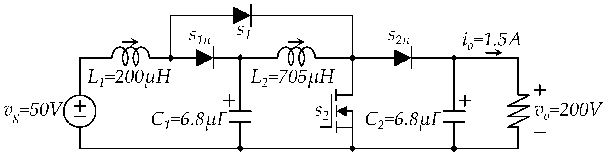
Figure 3. The quadratic boost converter with low buffer capacitor stress.
Electricity 07 00031 g003
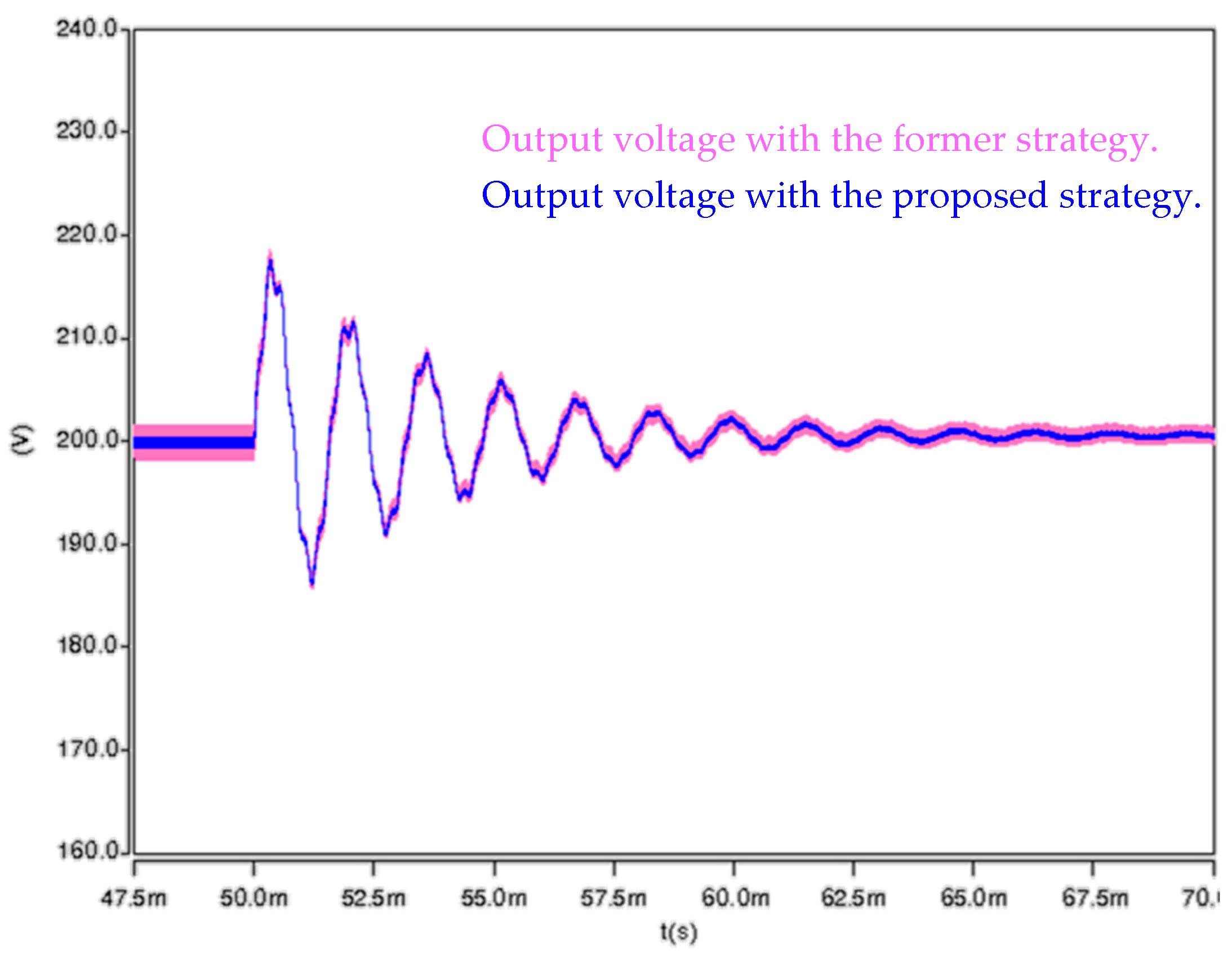
Figure 4. The low energy storage quadratic boost converter (LES-QBC).
Electricity 07 00031 g004
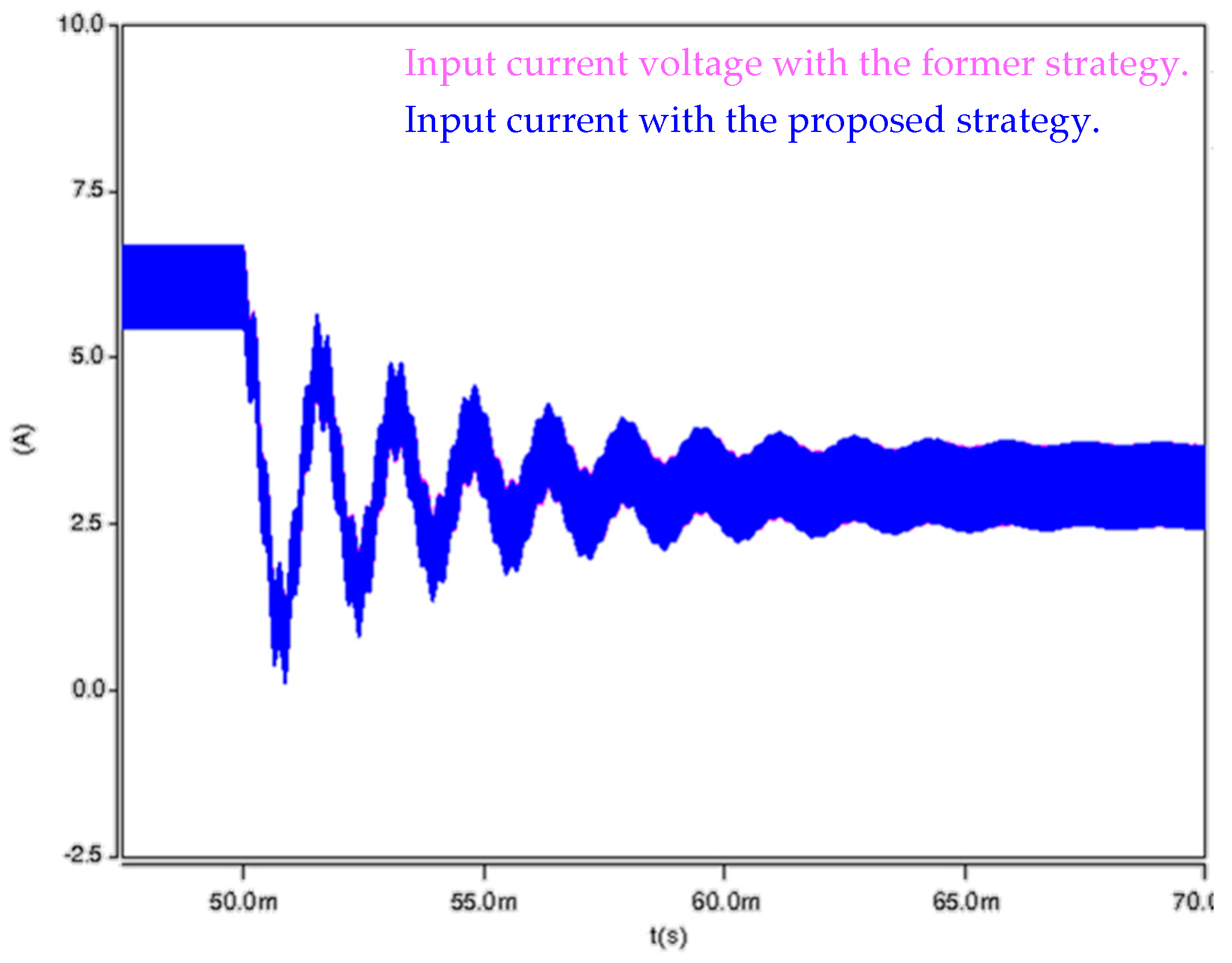
Figure 5. The Modified Quadratic Boost Converter.
Electricity 07 00031 g005
Figure 6. The SSQB Converter.
Electricity 07 00031 g006
Figure 7. The Quadratic Boost Converter based on Non-Series Energy Transfer (QBC-NSET).
Electricity 07 00031 g007
Figure 8. The interleaved boost converter.
Electricity 07 00031 g008
Figure 9. The input parallel output series connection of a boost converter and a high voltage three-switch converter.
Electricity 07 00031 g009
Figure 10. The interleaved series capacitor boost converter.
Electricity 07 00031 g010
Figure 11. The interleaved series capacitor boost converter.
Electricity 07 00031 g011
Figure 12. Switching states in the former switching strategy: (a) switches on; (b) switches off.
Electricity 07 00031 g012
Figure 13. Equivalent circuit of Figure 12b with the current through C2 indicated.
Electricity 07 00031 g013
Figure 14. The four possible switching states: (a) (0, 0), (b) (0, 1), (c) (1, 0), and (d) (1, 1).
Electricity 07 00031 g014
Figure 15. Switching behavior when D > 0.5: (a) switching signals; (b) switching states.
Electricity 07 00031 g015
Figure 16. Equivalent circuit of the state (0, 1); see Figure 15b bottom. The current through C2 is indicated.
Electricity 07 00031 g016
Figure 17. Switching behavior when D < 0.5: (a) switching signals; (b) switching states.
Electricity 07 00031 g017
Figure 18. Normalized output voltage ripple comparison.
Electricity 07 00031 g018
Figure 19. Experimental prototype.
Electricity 07 00031 g019
Figure 20. Input (blue) and output (green) voltages with (a) the former switching strategy, (b) the proposed operation with D = 0.45.
Electricity 07 00031 g020
Figure 21. Zoom into the output voltages with (a) the former switching strategy, (b) the proposed operation for D = 0.45.
Electricity 07 00031 g021
Figure 22. Input (blue) and output (green) voltages with (a) the former switching strategy, (b) the proposed operation with D = 0.50.
Electricity 07 00031 g022
Figure 23. Zoom into the output voltages with (a) the former switching strategy, (b) the proposed operation for D = 0.5.
Electricity 07 00031 g023
Figure 24. Input (blue) and output (green) voltages with (a) the former switching strategy, (b) the proposed operation with D = 0.55.
Electricity 07 00031 g024
Figure 25. Zoom into the output voltages with (a) the former switching strategy, (b) the proposed operation for D = 0.55.
Electricity 07 00031 g025
Figure 26. Inductor currents in both the former (a) and the proposed (b) switching strategy for D = 0.5.
Electricity 07 00031 g026
Figure 27. Inductor currents in both the former (a) and the proposed (b) switching strategy for D = 0.5.
Electricity 07 00031 g027
Figure 28. Voltage across capacitors in both the former (a) and the proposed (b) switching strategy for D = 0.5.
Electricity 07 00031 g028
Figure 29. Capacitors’ voltage ripple in both the former (a) and the proposed (b) switching strategy for D = 0.5.
Electricity 07 00031 g029
Figure 30. Summary of the fourth state variables in the converter in both the former (a) and the proposed (b) switching strategy for D = 0.5.
Electricity 07 00031 g030
Figure 31. Inductor currents in both the former (a) and the proposed (b) switching strategy for the output power change.
Electricity 07 00031 g031
Figure 32. Capacitors’ voltages in both the former (a) and the proposed (b) switching strategy for the output power change.
Electricity 07 00031 g032
Figure 33. Experimentally measured efficiency of the converter with both the former and the proposed switching strategy.
Electricity 07 00031 g033
Figure 34. The QBC-NSET with parameters.
Electricity 07 00031 g034
Figure 35. The cascaded boost converter with parameters.
Electricity 07 00031 g035
Figure 36. The traditional quadratic boost converter with parameters.
Electricity 07 00031 g036
Figure 37. Output voltage (voltage across capacitor C2) in the former and the proposed switching strategy.
Electricity 07 00031 g037
Figure 38. Input current (through inductor L1) in the former and the proposed switching strategy.
Electricity 07 00031 g038
Figure 39. Voltage across capacitor C1 in the former and the proposed switching strategy during the load rejection disturbance.
Electricity 07 00031 g039
Figure 40. Current through L2 in the former and the proposed switching strategy during the load rejection disturbance.
Electricity 07 00031 g040
Table 1. Normalized output voltage ripple in percentage.
Duty CycleNormalized Output Voltage Ripple in the Former StrategyNormalized Output Voltage Ripple in the Proposed Strategy
0.10.116111110.055
0.150.179558820.0825
0.20.24750.11
0.250.320833330.1375
0.30.400714290.165
0.350.488653850.1925
0.40.586666670.22
0.450.69750.2475
0.50.8250.275
0.550.974722220.42472222
0.61.1550.605
0.651.378928570.82892857
0.71.668333331.11833333
0.752.06251.5125
0.82.642.09
0.853.584166673.03416667
0.95.4454.895
Table 2. Parameters of the experimental setup.
ParameterValue
L1200 µH
L2705 µH
C1= C26.8 µF
Vo200 V
D0.45, 0.50, 0.55
Pout300 W
FS100 kHz
Disclaimer/Publisher’s Note: The statements, opinions and data contained in all publications are solely those of the individual author(s) and contributor(s) and not of MDPI and/or the editor(s). MDPI and/or the editor(s) disclaim responsibility for any injury to people or property resulting from any ideas, methods, instructions or products referred to in the content.