Article

Electro-Thermal Modeling and Thermal Analysis of High-Inertia Synchronous Condenser Converters

1
National Key Laboratory of Power Transmission and Transformation Equipment Technology, Chongqing University, Chongqing 400044, China
2
Chongqing City Management College, Chongqing 401331, China
*
Author to whom correspondence should be addressed.
Electricity 2025, 6(3), 53; https://doi.org/10.3390/electricity6030053
Submission received: 24 July 2025 / Revised: 9 September 2025 / Accepted: 12 September 2025 / Published: 15 September 2025

Abstract

High-inertia energy storage synchronous condenser (HI-ES-SC) is operated through rotor-excited variable-speed mechanisms to provide grid power support. Power devices are exposed to alternating electro-thermal stresses, with significant implications for system reliability. Therefore, an electro-thermal modeling approach is developed for the converter of HI-ES-SC during power support operation. Switching dynamics and conduction states are incorporated in the model. A theoretical framework is established to analyze loss mechanisms and junction temperature evolution. A coupled electro-thermal model is constructed, accounting for temperature-dependent thermal network parameters. A numerical solution is proposed to enable co-simulation of condenser–converter systems. The simulation results indicate that the error in thermal parameter estimation remains below 10%. Key findings are summarized as follows: Under active power support, the peak junction temperature is observed to reach 81.69 °C during synchronous speed crossing, accompanied by notable low-frequency thermal accumulation. The derived operational-thermal correlation provides critical guidance for optimal thermal design and device selection.

1. Introduction

With the large-scale development of new energy and ultra-high voltage direct current (UHVDC) in China, the trend of power system electrification is continuously intensifying. As a result, voltage and frequency problems have become increasingly prominent [1,2,3]. Compared with static reactive power compensation devices, synchronous condensers possess autonomous reactive power response characteristics during faults. Their high overload capability and high reliability enable them to better satisfy the reactive power demands of UHVDC systems and alleviate the impacts of high-penetration power system electrification on system stability [4]. However, the existing synchronous condensers cannot provide active power support to the system and lack oscillation-damping capability.
In recent years, researchers have proposed a high-inertia energy storage synchronous condenser (HI-ES-SC) [5], which has gained significant attention due to its combined capabilities in providing voltage, inertia, and frequency support. The grid-side converter of the HI-ES-SC employs a neutral-point-clamped (NPC) three-level topology [6], while the machine-side converter employs an active neutral-point-clamped (ANPC) three-level topology [7,8,9]. Its power semiconductor device is the Integrated Gate-Commutated Thyristor (IGCT). The differences in structural and operational characteristics between IGBT and IGCT are shown in Table 1. This condenser adopts a doubly fed induction machine structure, achieving power support to the system through variable-speed rotor excitation control. As a key component in the HI-ES-SC electrical system, the converter incurs substantial costs. It also exhibits high failure rates. During operation, the HI-ES-SC frequently switches operating conditions. It can operate with a large slip and under variable speed. Changes occur in active power, reactive power, rotor current, and frequency. These variations complexly affect the converter’s thermal behavior. However, few studies address the thermal characteristics of HI-ES-SC converters. Establishing a relationship between electrical quantities and junction temperature in HI-ES-SC is essential. Such a correlation would offer theoretical support for thermal design, component selection, and real-time junction temperature monitoring.
Currently, most research on electro-thermal coupling modeling of converters takes Insulated Gate Bipolar Transistors (IGBTs) as the research object. In [10], the authors investigate the loss and junction temperature distribution of an IGBT three-level converter. In [11], the authors take doubly fed wind turbines as the research object, conduct electro-thermal coupling modeling of the IGBT converter, and propose a junction temperature fluctuation suppression strategy based on the IGBT junction temperature calculation. In [12], the authors establish a lifetime assessment model for the photovoltaic inverters. In research related to synchronous condensers. In [13], the authors analyze the temporal and spatial distribution characteristics of temperature rise in a synchronous machine using a lumped-parameter method. In [14], the authors investigate the effects of different steady-state operating conditions on the transient temperature rise during single-phase short circuits in a synchronous condenser. However, the loss, thermal resistance, and heat capacity parameters in the above models are often regarded as fixed values. Less consideration is given to the fluctuations in loss, thermal resistance, and heat capacity caused by the interactions between the device’s electrical and material parameters. Moreover, the HI-ES-SC utilizes IGCT devices, and there are significant differences in its operation mode. Therefore, the aforementioned studies cannot directly reflect the temperature rise characteristics of the HI-ES-SC.
The existing methods for modeling the electro-thermal coupling of IGCT can be sorted into three types. The first type is aggregate element modeling [15,16,17,18]. It has a fast simulation speed but cannot be used to study the transient variation in HI-ES-SC electrical quantities. The second type is finite element modeling (FEM) [19,20,21]. It has higher accuracy but a slower simulation speed. The third type is the RC thermal network model. This model is based on the thermoelectric analogy principle and estimates the device junction temperature by calculating losses. It combines the advantages of fast simulation speed and relatively high accuracy. In [22], the authors propose a Temperature-sensitive Electrical Parameter (TSEP)-based junction temperature extraction method for IGCT and establish a dynamic electro-thermal coupling model. In [23], the authors propose a radial electro-thermal coupling model by segmenting the ring of the IGCT chip. In [24], the authors conduct research on accelerated aging tests for IGCT devices. In [25], the authors propose calculation methods for switching loss and conduction loss of IGCTs in three-level converters. However, most of these studies primarily focus on investigating the heat generation characteristics of devices or converters operating independently. They cannot reflect the temperature rise characteristics of the HI-ES-SC under complex operating conditions.
In summary, the main work carried out in this paper is as follows: First, based on the topology of the NPC three-level converter, the switching actions and current paths of the devices are studied. The variations in rotor current and temperature rise during HI-ES-SC power output are analyzed. Then, based on the characteristics of the IGCT, an electro-thermal coupling model of the converter is established. A calculation method for the thermal network parameters of this electro-thermal coupling model is proposed, and the solution process for the model is provided. Subsequently, the proposed model is compared and validated against a traditional linear model and an FEM to verify its effectiveness. Finally, by establishing a co-simulation model integrating HI-ES-SC dynamics and electro-thermal coupling, the temperature rise effect of the converter when the HI-ES-SC provides power support to the system is analyzed. The innovations of this paper are as follows: (1) The linkage between the junction temperature variation in the HI-ES-SC under different operating conditions and its operational parameters is analyzed by combining theoretical analysis and case studies. (2) The proposed model accounts for the interactions between the thermal network parameters and the junction temperature, improving the accuracy of junction temperature calculation. (3) Through simulation analysis, the pattern of junction temperature variation during HI-ES-SC power output is studied, revealing the heat accumulation effect generated when the HI-ES-SC speed decreases to the vicinity of the synchronous speed.

2. Operating Characteristics of HI-ES-SC

Figure 1 shows the structure of the HI-ES-SC, and its operation modes are mainly divided into two types: long-time working system and short-time working system. The long-time working system consists of two operation modes: no-load operation mode with speed control and phase regulation operation mode with reactive power control. The long-time operation system is mainly applied to the operation during the steady state of the power grid. When a power shortage or excess occurs in the grid due to faults or other reasons, the HI-ES-SC enters the short-time operation system to provide emergency support for the system. Under short-time operation, when the system has a power shortage or excess, HI-ES-SC can provide short-time active support through speed regulation, and when the system has a reactive power shortage or excess, HI-ES-SC can provide short-time high-frequency reactive power support.
The HI-ES-SC adopts a doubly fed asynchronous generator with AC excitation, and the voltage and frequency support control is realized by regulating the rotor current amplitude and phase through the excitation converter. The machine-side converter control system usually adopts vector control with stator magnetic chain orientation, and the relationship between the stator output active power and reactive power of the HI-ES-SC and the rotor d- and q-axis currents is as follows:
P s = 3 L m u s m 2 L s i r q Q s = 3 u s m ψ s m 2 L s 3 L m u s m 2 L s i r d
where L m is the excitation inductance; L s is the equivalent inductance of the stator; i r d and i r q represent the d- and q-axis components of the rotor current, respectively; u s m is the stator voltage magnitude; and ψ s m is the stator magnetic chain magnitude.
In the case of double closed-loop vector control, the reference values of d- and q-axis voltage of HI-ES-SC can be written as follows:
u r d * = k i p ( i r d * i r d ) + k i i ( i r d * i r d ) d t σ ω p L r i r q u r q * = k i p ( i r q * i r q ) + k i i ( i r q * i r q ) d t + σ ω p L r i r d
where u r d * and u r q * are the machine-side converter voltage reference value of d and q components, respectively; i r d * and i r q * are the machine-side converter current reference value of d and q components, respectively; and k i p and k i i are the proportional and integral coefficients of the inner-loop PI controller.
The rotor d-axis current reference value can be determined by the given reactive power reference value:
i r d * = k o p ( Q s * Q s ) + k o i ( Q s * Q s ) d t
where Q s * is the reactive power reference value, and k o p and k o i are the outer loop proportional and integral coefficients.
In speed control mode, the rotor q-axis current can be written as follows:
i r q * = 2 L s 3 L m ψ s m k o p ( ω r * ω r ) + k o i ( ω r * ω r ) d t
where ω r * is the reference value of rotational speed.
The converter for HI-ES-SC consists of machine-side and grid-side converters. Among them, each phase of the grid-side converter consists of the NPC three-level converter unit shown in Figure 2a, and each unit contains V T 1 , V T 2 , V T 3 , and V T 4 , four IGCT main switches; V D 1 , V D 2 , V D 3 , and V D 4 , four freewheeling diodes; and V D T 1 and V D T 2 , two clamp diodes. The converter has three switching states: when V T 1 and V T 2 are on, V T 3 and V T 4 are off, the corresponding level is 1 / 2 U d c , and the switching state is recorded as p. When V T 2 and V T 3 are on, V T 1 and V T 4 are off, the corresponding level is 0, and the switching state is recorded as O. When V T 3 and V T 4 are on, V T 1 and V T 2 are off, the corresponding level is 1 / 2 U d c , and the switching state is recorded as N. Under low-frequency conditions, the switching time of the switches on the inner side of the NPC topology is much larger than that of the outer one, and the outer switches will undergo more turn-on and turn-off, leading to uneven losses between the inner and outer switches. Therefore, the NPC three-level topology is used only in the grid-side rectifier part.
The topology of the machine-side converter is shown in Figure 2b, compared with the NPC topology, ANPC expands the freewheeling path and improves the loss distribution of the device by adding two additional switches V T 5 and V T 6 . When the ANPC switches the current level, each level switching has two current switching paths. The devices involved in the switching process are shown in Table 2. Considering the three-phase symmetry of the NPC converter and the symmetry of the four switching processes of the single bridge arm [8,12], this paper selects V T 1 , V T 2 , V T 5 , V D 3 , V D 4 , and V D T 1 as the object.
Under short-time operation, take the rotor current i r > 0 and the current switching path 1 as an example. When the switching state is P, V T 1 and V T 2 turn on and generate conduction loss. When P changes to O, V T 1 turns off and generates shutdown loss, V D 5 and V T 2 turn on. When the switching state is O, V D 5 and V T 2 conduct to generate conduction loss. When O changes to N, V T 2 and V D 5 turn off to generate a shutdown loss, and the freewheeling diodes V D 3 and V D 4 turn on. When the switching state is N, the freewheeling diodes V D 3 and V D 4 conduct to produce conduction loss. When N changes to O, the freewheeling diodes V D 3 and V D 4 turn off to produce shutdown loss, and V T 5 and V T 2 turn on to produce turn-on loss. When O changes to P, V T 5 turns off to produce shutdown loss, and V T 1 conducts to produce turn-on loss. The rotor current i r < 0 is analyzed in a similar way for current switching path 2.
When the HI-ES-SC outputs active power, the speed of the HI-ES-SC decreases, and the turn-on loss and switching loss increase with the rotor current amplitude, causing the converter junction temperature to rise. In addition, since the no-load speed of the HI-ES-SC is at supersynchronous speed, the speed drop process will pass through the low-frequency operation interval of the converter, and at this time, the too-low operation frequency of the converter will prolong the continuous rise time of the junction temperatures of V T 1 , V T 2 , V D 3 , V D 4 , and V T 5 , which will result in the junction temperature fluctuations and spikes.
Maintaining the turndown rate and machine end voltage unchanged, without changing the stator active output, the relationship between the rotor current change amount Δ I ˙ r and the stator reactive power change amount Δ Q s is as follows [25]:
Δ I ˙ r = ( R s + j X s ) 3 X m U s Δ Q s
where R s and X s are stator resistance and reactance, X m is excitation reactance, and U s is stator voltage. From Formula (5), it can be seen that when HI-ES-SC outputs reactive power, the increase in rotor current will cause the converter loss to increase, which leads to the junction temperature rise.

3. Electro-Thermal Coupling Modeling of the HI-ES-SC Converter

3.1. Calculation Model of Converter Junction Temperature

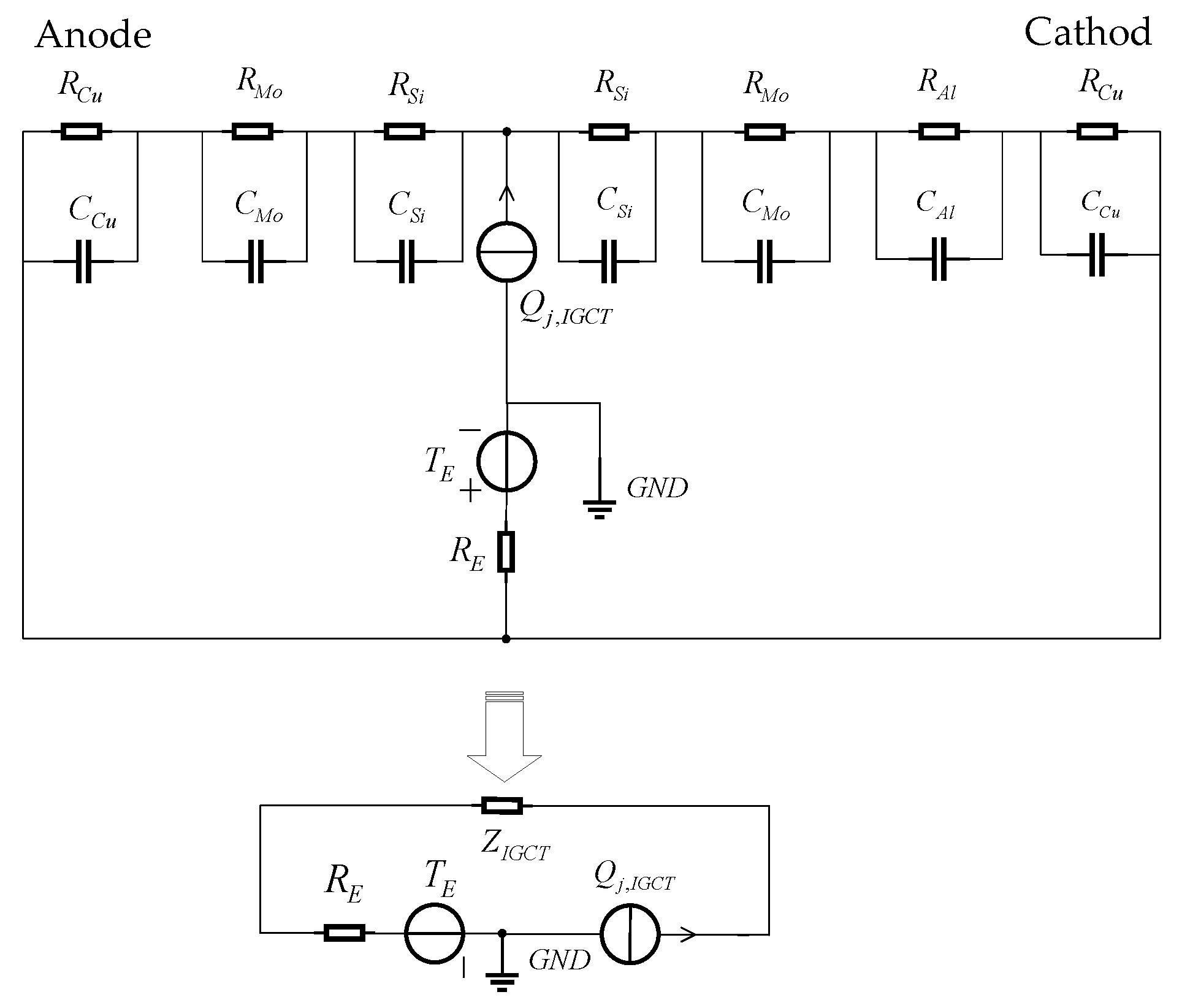
The switching device of the HI-ES-SC is an IGCT. The chip exterior of the IGCT consists of cathode/anode molybdenum plates, aluminum plates, and copper plates. Since the chip and the two-pole molybdenum plate realize electrical contact through axial pressure, the main heat dissipation direction is axial [22]. Based on this structural feature, this paper adopts the thermal network modeling method based on the first-order lumped parameters, and the established IGCT thermal network model is shown in Figure 3. Among them, R S i , R M o , R A l , R C u are the thermal resistances of silicon wafer, molybdenum plate, aluminum plate, and copper plate. C S i , C M o , C A l and C C u are the thermal capacitance of silicon wafer, molybdenum plate, aluminum plate, and copper plate. T E and R E are the ambient temperature and the thermal resistance of the heat sink. To simplify the model, the multilayer structure between points A and B (containing R S i , R M o , R A l , R C u , C S i , C M o , C A l , and C C u ) in series-parallel is equivalent to the integrated thermal impedance of the IGCT chip to the environment Z I G C T .
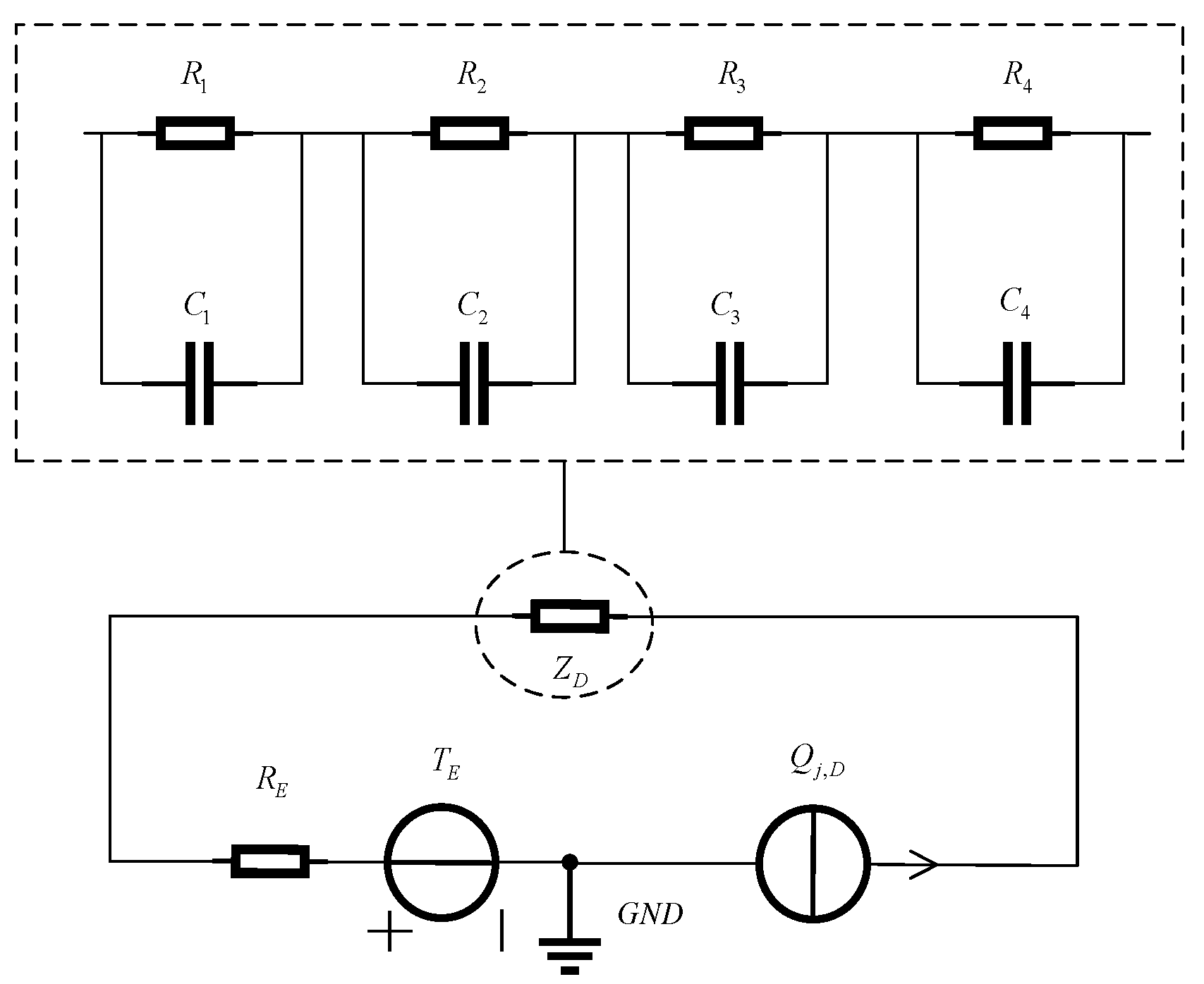
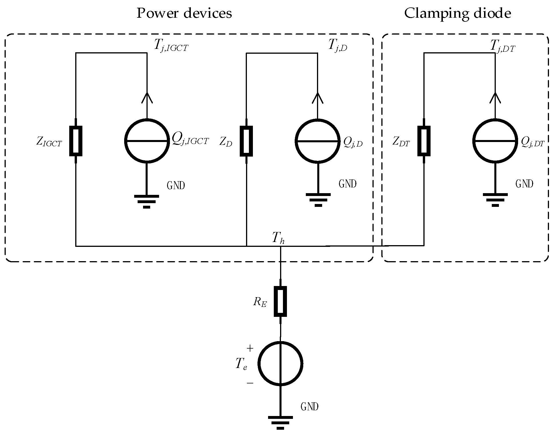
The modeling method proposed in [26] is used to model the corresponding diode thermal network for clamp diode V D T 1 and clamp diodes V D 3 and V D 4 , as shown in Figure 4. In the figure, R 1 , R 2 , R 3 , and R 4 are the thermal resistances of the diodes with four different materials from inside to outside. In the figure, C 1 , C 2 , C 3 , and C 4 are the thermal capacitances of the diode with four different materials from inside to outside. Based on the IGCT model in Figure 3 and the diode model in Figure 4, the final complete thermal network model of the converter is established as shown in Figure 5. Among them, Q j , D and Z D correspond to the loss and thermal impedance of the freewheeling diodes V D 3 and V D 4 of the converter, Q j , D T and Z D T correspond to the loss and thermal impedance of the clamp diode V D T 1 of the converter, Q j , I G C T and Z I G C T correspond to the loss and thermal impedance of the IGCT device V T 1 of the converter. T h is the heat sink temperature.
The thermoelectric analog method is used to simulate the flow of heat. The loss Q , temperature T, and thermal impedance Z t h analogous to the current I, voltage U, and impedance Z, can be obtained for the three kinds of devices of the electro-thermal coupling model:
T j , I G C T = Q j , I G C T Z I G C T + T h T j , D = Q j , D Z D + T h T j , D T = Q j , D T Z D T + T h
where T j , I G C T is the junction temperature of IGCT V T 1 , V T 2 , V T 5 ; T j , D is the junction temperature of the freewheeling diodes V D 3 and V D 4 ; T j , D T is the junction temperature of the clamp diode V D T 1 ; and T h is the heat sink temperature. In order to visualize the junction temperature of the converter and provide a reference basis for device selection, the maximum value of T j is taken as the junction temperature of the converter from T j , I G C T , T j , D and T j , D T .

3.2. Calculation Method of Converter Thermal Network Parameters

3.2.1. Heat Parameters

In the electro-thermal coupling model, the losses of the IGCT, the freewheeling diode, and the clamping diode can be expressed as the sum of the conduction loss and the switching loss, which is calculated as follows:
Q j = Q c o n , j + Q s w t i c h , j
where Q j is the device loss, Q c o n , j is the conduction loss, and Q s w t i c h , j is the switching loss.
The conduction loss of the device Q c o n , j is as follows:
Q c o n , j = α 0 π u o n , i i T d t
where u o n , i is the forward voltage and α is the duty cycle. In a single cycle, the on-state duty cycle is α = t o n / t c . t o n is the conduction time of the device.
Under the SPWM modulation strategy, the on-state duty cycle of the device is shown in Table 2. m is the modulation index, and φ is the power factor angle. i T is the load current of the converter, which can be written as follows:
i T = I r sin ( ω i t )
where I r is the HI-ES-SC rotor’s current amplitude. ω i is the current angular frequency.
When the device is conducting, the forward voltage is divided into two parts: the junction voltage u n o d e and the voltage drop u d r i f t :
u o n , j = u n o d e + u d r i f t
The junction voltage and the voltage drop each play a dominant role in different regions [22]. Near the p+n junction, the junction voltage dominates. In the n drift region, the voltage drop dominates. At this point, the formula for u n o d e is as follows:
u n o d e = k T q ln ( p L n R ) k T q ln n i 2
where k is the Boltzmann constant, which can take a typical value of 1.38 × 10⁻²³ J/K. T is the temperature. q is the electron charge, which can take a typical value of 1.6 × 10⁻¹⁹ C. pL is the hole concentration near the neutral substrate near the p+ n junction. nR is the electron density on the n+ side of the substrate. ni is the carrier concentration.
Under the effect of forward voltage, electrons diffuse from the N region to the P region and holes diffuse from the P region to the N region, and the carrier concentration in the junction region increases, forming a large injection condition. μn, μp, Dn, Dp, n i and T have a power-law relationship [23]. At this point, udrift is calculated as follows:
u d r i f t = w B 2 ( μ n + μ p ) L a tanh ( w B 2 L a ) 2 H j / q L a = D a τ H L D a = 2 D n D p D n + D p μ n = 1400 × ( T / 300 ) 2.5 μ p = 500 × ( T / 300 ) 2.5 D n = μ n k T / q D p = μ p k T / q n i = 3.88 × 10 16 × T 1.5 × e 7000 / T
where wB is the width of the n layer. μn and μp are the mobilities of free electrons and holes. La is the ambipolar diffusion length. j is the total current density. H is the emitter parameter, which can take a typical value of 2 × 10⁻¹⁴ cm4/s. Dn and Dp are the diffusion coefficients of free electrons and holes. τ H L is the carrier lifetime under high-level injection conditions.
The switching loss Q s w t i c h , j is calculated as follows:
Q s w i t c h , j = 0 t s w i t c h Q o n , j + Q o f f , j t c d t
where Q c o n , j and Q o f f , j are the turn-on loss and turn-off loss, t s w i t c h is the total time of the continuous switching region, and t c is the carrier cycle.
From the chip datasheet, the switching loss has a linear relationship with the load current i T :
Q o n , j = k k _ o n i T + k c _ o n Q o f f , j = k k _ o f f i T + k c _ o f f
where k k _ o n , k c _ o n , k k _ o f f , and k c _ o f f can be obtained from the chip datasheet, and the values of 3.33 × 10 4 , 0.533, 8.5 × 10 3 , 0.4 are adopted in this paper.

3.2.2. Thermal Capacitance Parameters

Calculated according to the definition of heat capacity:
C = ρ c A l
where C , ρ , and c are the heat capacity, density, and specific heat capacity of the converter material at the node of the thermal network. The specific heat capacity of the material is affected by the temperature, which can be obtained by checking Table 2 to obtain the value of the corresponding temperature. l and A are the length of the material and the radial cross-sectional area.

3.2.3. Thermal Resistance Parameters

According to the definition, the thermal resistance of the material is as follows:
R = l A λ
where R and λ are the thermal resistance and thermal conductivity of the converter at the thermal network node. The thermal conductivity of the material is affected by temperature, and the value corresponding to the temperature can be obtained by looking up Table 3.
Heat sink thermal resistance R E includes three parts: substrate thermal conductivity thermal resistance R c o n d , convection thermal resistance R c o n v , and substrate diffusion thermal resistance R s p :
R E = R c o n d + R c o n v + R s p
The heat generated by the device is transferred to the fins through the thermal conductive resistance of the substrate, and R c o n d is expressed as follows:
R c o n d = t b B c o n d k A l
where t b is the thickness of the IGCT base plate, B c o n d is the contact area between the heat sink and the fins, and k A l is the thermal conductivity of aluminum.
The thermal resistance between the surface of the fin base of the heat sink and the air R c o n v is given by:
R c o n v = 1 η h x B c o n d
where η is the heat dissipation efficiency, and h x is the convective heat transfer coefficient. The convective heat transfer coefficient of the heat sink is complicated and is calculated by the following formula:
h x = k f N v s s N v s = f / 8 R e s 1000 P r 1 + 12.7 f / 8 0.5 P r 2 / 3 1 R e s = ρ v s D h μ D h = 2 s l w s + l w f = 0.79 ln R e s 1.64 2
where k f is the air thermal conductivity, N v s is the Nusselt number, s is the fin spacing, f is the friction coefficient, P r is the Prandtl number, R e s is the Reynolds coefficient, v s is the air flow rate, D h is the coefficient of channel structure, and l w is the length of the fins.
The expression of diffusion thermal resistance R s p is as follows:
R s p = 1 ε π k A l r 1 tanh π + 1 ε π t b r 2 + π + 1 ε π B i 1 + π + 1 ε π B i tanh π + 1 ε π t b r 2
where ε is the characteristic radius, r 1 is the heat source equivalent radius, r 2 is the substrate equivalent radius, and B i is the Biot number. The calculation is as follows:
ε = r 1 r 2 r 1 = B c o n d π r 2 = B π B i = h x r 2 k A l
The loss of the electro-thermal coupling model is affected by the forward voltage, rotor current, and rotational speed, in which the rotor current and rotational speed depend on the HI-ES-SC working condition, and the forward voltage is affected by the parameters of the IGCT chip itself and the external temperature. At the same time, the forward voltage, resistivity and heat capacity of the electro-thermal coupling model are all affected by the external temperature, which are important influencing factors of the model nonlinearity. The geometry and airflow parameters of Equations (17)–(22) are shown in Table 4.

3.3. Real-Time Calculation Method of Junction Temperature of Converter Electro-Thermal Coupling Model

The HI-ES-SC converter has a large capacity and complex structure, with variable operating conditions, making it difficult to conduct temperature rise experiments. In addition, the traditional electro-thermal coupling model solution is often based on the determined loss, thermal resistance, and thermal capacitance parameters for junction temperature calculation. However, as shown in Formulas (12), (15) and (16), it can be realized that the conduction loss, thermal resistance, and thermal capacitance of the actual device are affected by the temperature. Therefore, the above parameters are fluctuating during the operation of HI-ES-SC. Based on the above considerations, this paper adopts a nonlinear iterative method to solve the electro-thermal coupling model. The specific flow is shown in Figure 6. The values of Δ t = 1 ms and ε = 0.001 are adopted in this paper.
To ensure the accuracy of the proposed electro-thermal model, a nonlinear iterative computation process is implemented until all parameters achieve full convergence. The procedure is initiated by assigning the preset ambient temperature and the rotor current measured during the startup of the High-Inertia Electro-thermally Synchronous Condenser (HI-ES-SC) as the initial inputs. These values are substituted into Equations (7) to (22) to compute the initial power loss, thermal resistance, and thermal capacitance parameters of the lumped parameter thermal network. Using these derived parameters, the updated temperature vector T(s) is obtained by solving the governing thermal equation given in Formula (6).
In the subsequent step, the power loss, thermal resistance, and thermal capacitance are recalculated and adjusted according to the new temperature distribution T(s). These updated values are again substituted into Formula (6) to solve for the next temperature state vector T(s + 1). This correction–iteration loop continues until the element-wise absolute difference between consecutive temperature vectors T(s) and T(s + 1) falls below a predefined convergence threshold ε.
Once the iterative process converges, the model proceeds to compute real-time junction temperature across the power module. The final temperature result T(s + 1) from the iteration serves as the initial state for the subsequent transient temperature rise simulation. During this phase, the thermal network parameters are dynamically updated according to real-time variations in operational conditions, including junction temperature, heat sink airflow velocity, and rotor current magnitude. The simulation advances with a fixed time step Δt until the entire designated duration T (representing the total transient process time) is completed, ultimately yielding the transient temperature profile of the converter thermal network.

4. Simulation of Electro-Thermal Coupling Model and Temperature Rise in HI-ES-SC

4.1. Validation of the Electrical-Thermal Coupling Model of the Converter

To verify the proposed model’s accuracy, this paper compares and analyzes the proposed model with the traditional linear model [27] and the FEM [28]. Under the test conditions of ambient temperature of 30 °C and wind rate of 0, the results of RC parameter calculations of the three models are shown in Table 5. The comparison results show that the accuracy of the proposed model in thermal resistance calculation is significantly better than that of the linear model, and the accuracy of heat capacity calculation is also improved compared with the linear model. The linear model has a deviation of up to 84.67% in the thermal resistance calculation of silicon because it does not take into account the interactions of temperature, electrical parameters, and material parameters. In contrast, the deviations in thermal resistance and heat capacity parameters of the model proposed are less than 10%.
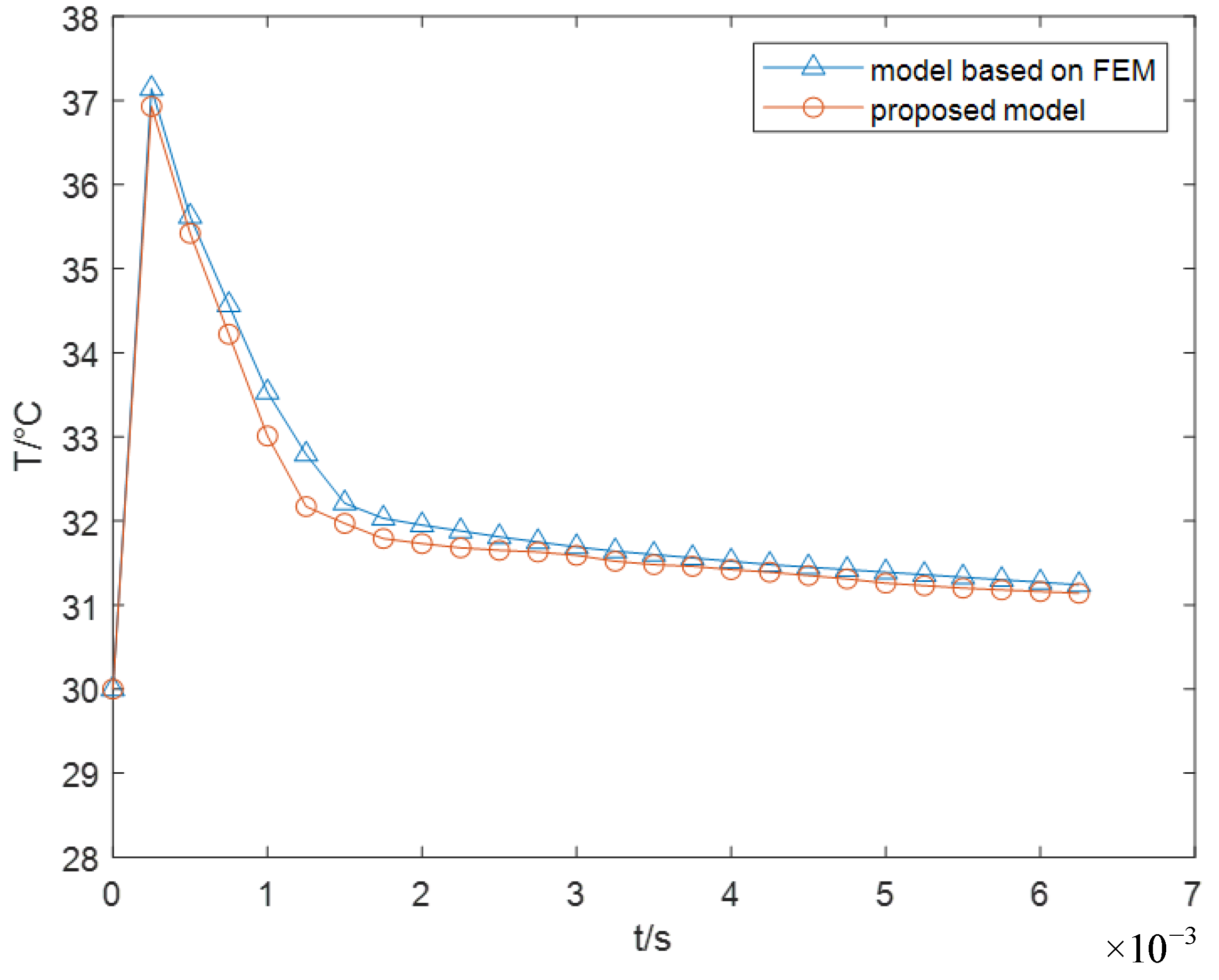
Under the same ambient temperature with 160 Hz switching frequency, junction temperature curves of the proposed and FEM are shown in Figure 7. During the single switching test, since switching loss of IGCT is more significant than conduction loss, junction temperature curve shows a phenomenon of rapid rise followed by gradual cooling. In terms of accuracy, the deviation in junction temperature of the proposed model from FEM is less than 2%. Combined with thermal resistance and heat capacity data in Table 3, thermal resistance of the proposed model is larger than that of FEM, so the peak value is slightly higher; heat capacity is smaller, so the temperature change rate is slightly faster than FEM. Figure 8 shows the peak temperatures and the temperatures corresponding to the maximum deviation in both the proposed model and the finite element model under different wind speeds. At wind speeds of 0, 0.5, 1, 1.5, and 2 m/s, the peak deviations in junction temperature are 0.57%, 0.19%, 0.20%, 0.68%, and 0.84%, respectively, while the maximum deviations are 1.89%, 2.6%, 1.58%, 1.13%, and 1.68%. These results indicate that despite deviations of less than 10% in the thermal resistance and thermal capacitance parameters of the proposed model, both the peak and maximum deviations remain below 3%. This demonstrates the model’s low sensitivity to parameter variations and its ability to accurately reflect the junction temperature of the device under varying wind conditions.

4.2. Model Validity Verifications of Junction Temperature

To enhance the relevance of the proposed method to practical engineering applications, additional on-site experimental comparisons were included. This paper compares the proposed model with the experimental results reported in References [22,29].

4.2.1. Single Switch Test

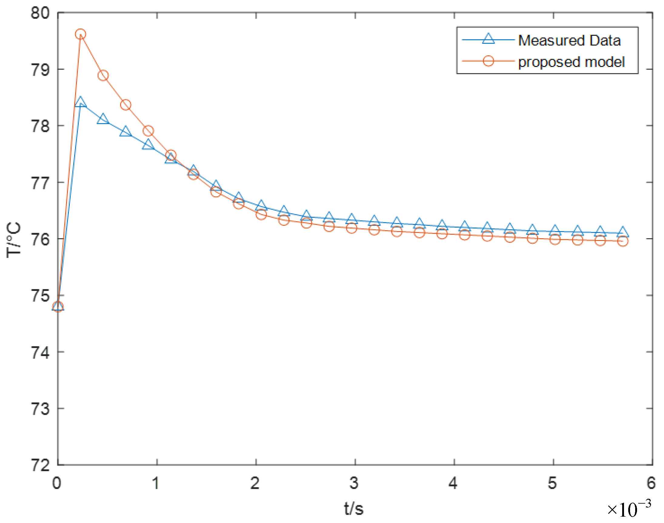
Reference [22] employed an IGCT model 5SHY35L4521 and conducted a single switching test at 175 Hz under the following conditions: UDC = 2.2 kV, Ir = 1.5 kA, initial temperature = 74.8 °C, and vs. = 0 m/s. Using the same IGCT device parameters from Reference [22] as inputs in Figure 6, the junction temperature during the single switching event was calculated by substituting these into Equations (7) to (22), following the identical testing procedure outlined in Section 4.1. Figure 9 shows the junction temperature measured in the experiment from Reference [22] together with that calculated by the proposed method using the same experimental parameters. The proposed method achieved both a maximum error and a peak error of 1.6% during the single switching test.

4.2.2. 3-H Junction Temperature Test

For validation based on Reference [24], a CAC 5000-45 Plus IGCT device was used. Its dimensions were taken from the corresponding datasheet, and a chip junction temperature test was performed under the same conditions as in Reference [24]: vs. = 0 m/s, UDC = 2.5 kV, switching frequency = 150 Hz, and ambient temperature = 30 °C. These parameters were used as inputs in Figure 6 and substituted into Equations (7) to (22). The same test method described in Section 3.3 was applied to calculate the peak junction temperature continuously for 3 h. The results summarized in Table 6 show that after 3 h of continuous operation under rotor currents of 3.5 kA and 4 kA, the junction temperature errors were 0.5% and 3.3%.

4.3. Analysis of Converter Loss and Junction Temperature

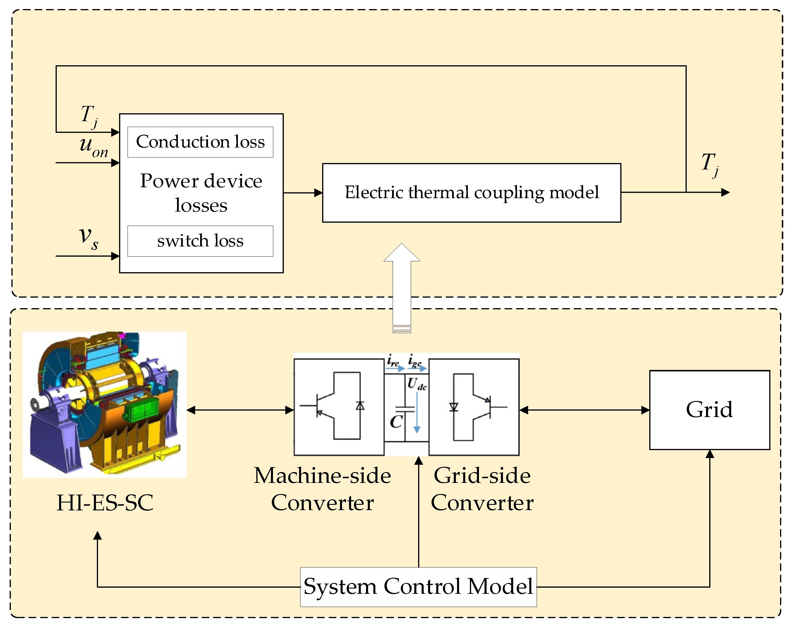
To analyze electrical characteristics and temperature rise patterns under different operating conditions, a Simulink-PLECS co-simulation model, as shown in Figure 10, was established. In the figure, when the Simulink model outputs active power/reactive power to the grid through HI-ES-SC, the rotor current amplitude, frequency, and other electrical signals of the converter are connected to the PLECS model, which completes the calculation of junction temperature and loss based on the material parameters of the device and the electrical signals of the converter obtained. The parameters of the HI-ES-SC simulation model used are shown in Table 7. The device parameters are provided by the manufacturer [29], and the heat sink is adopted from the literature [30], with the heat sink parameters of the same packaged module. Considering the energy storage requirement of the HI-ES-SC, the no-load speed is usually set at a supersynchronous speed. Meanwhile, in order to be more favorable for releasing the effective stored energy and exploiting the asynchronous torque characteristics, the rotational speed should be set in the interval of higher asynchronous torque [4]. Therefore, the no-load speed of the HI-ES-SC is set at 1.05 p.u.
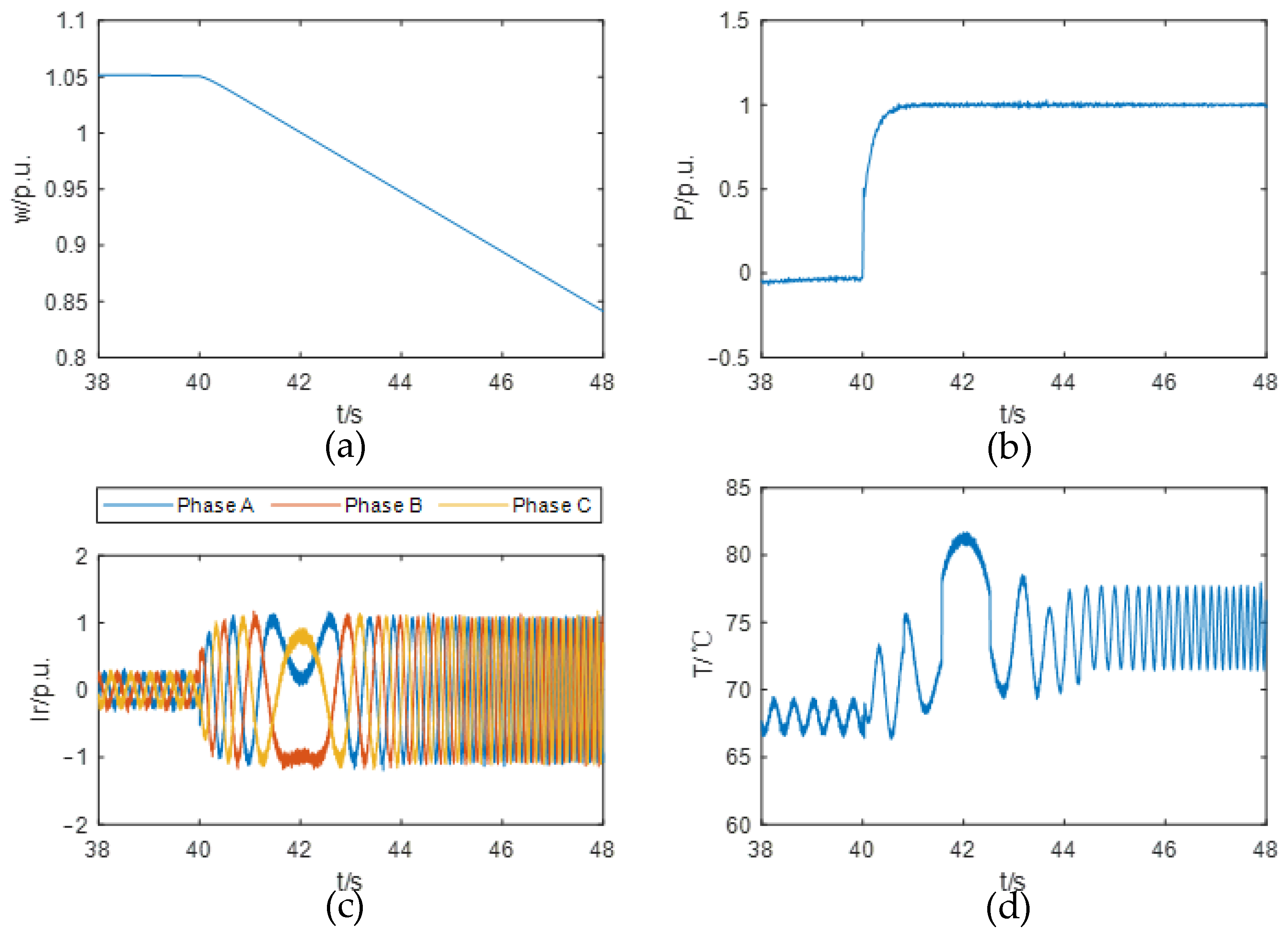
Figure 11 shows the curves of rotational speed, active power, rotor current, and junction temperature of the converter when the HI-ES-SC continuously outputs 1.0 p.u. active power. The rotational speed decreases from 1.05 to 0.85 p.u. when the HI-ES-SC continuously outputs 1.0 p.u. active power starting from 40 s. The rotational speed decreases from 1.05 to 0.85 p.u. during this period. During the speed drop, the amplitude of rotor current gradually increases, and the amplitude of converter junction temperature fluctuation increases. At about 42 s, the HI-ES-SC speed decreases to near the synchronous speed, the converter operates at low frequency, the frequency of junction temperature fluctuation becomes smaller, and the converter junction temperature reaches a maximum value of 81.69 °C.
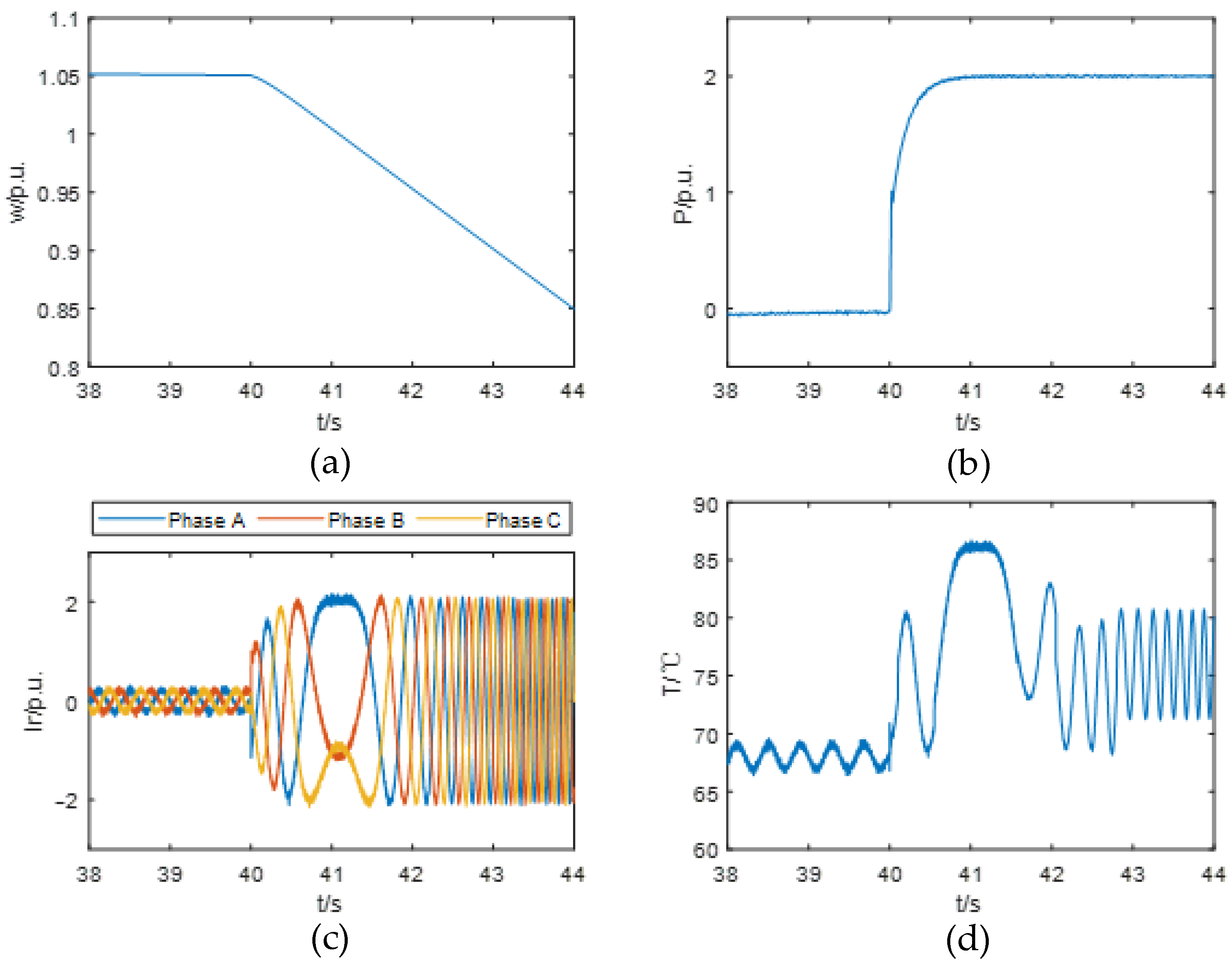
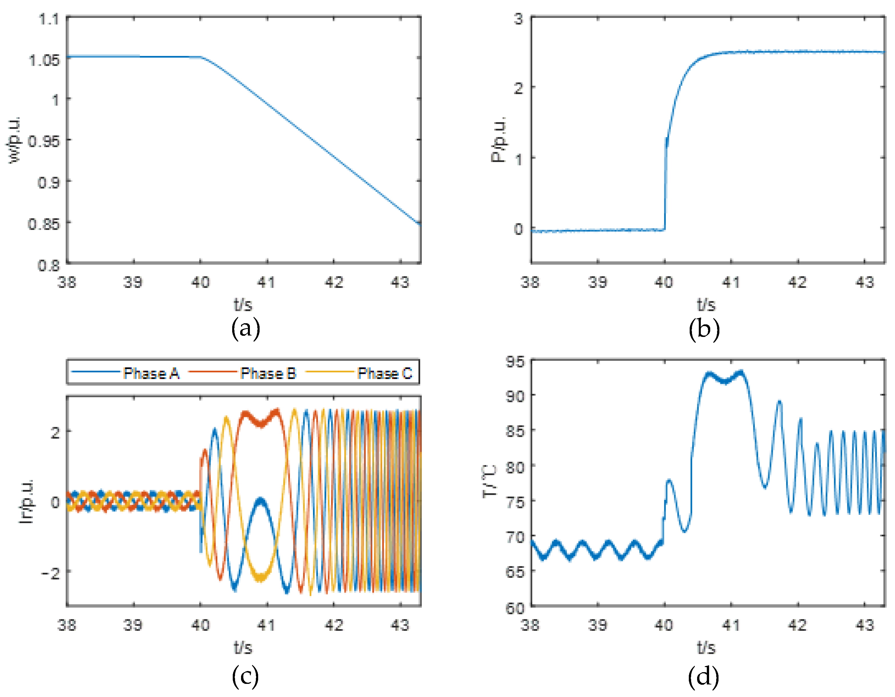
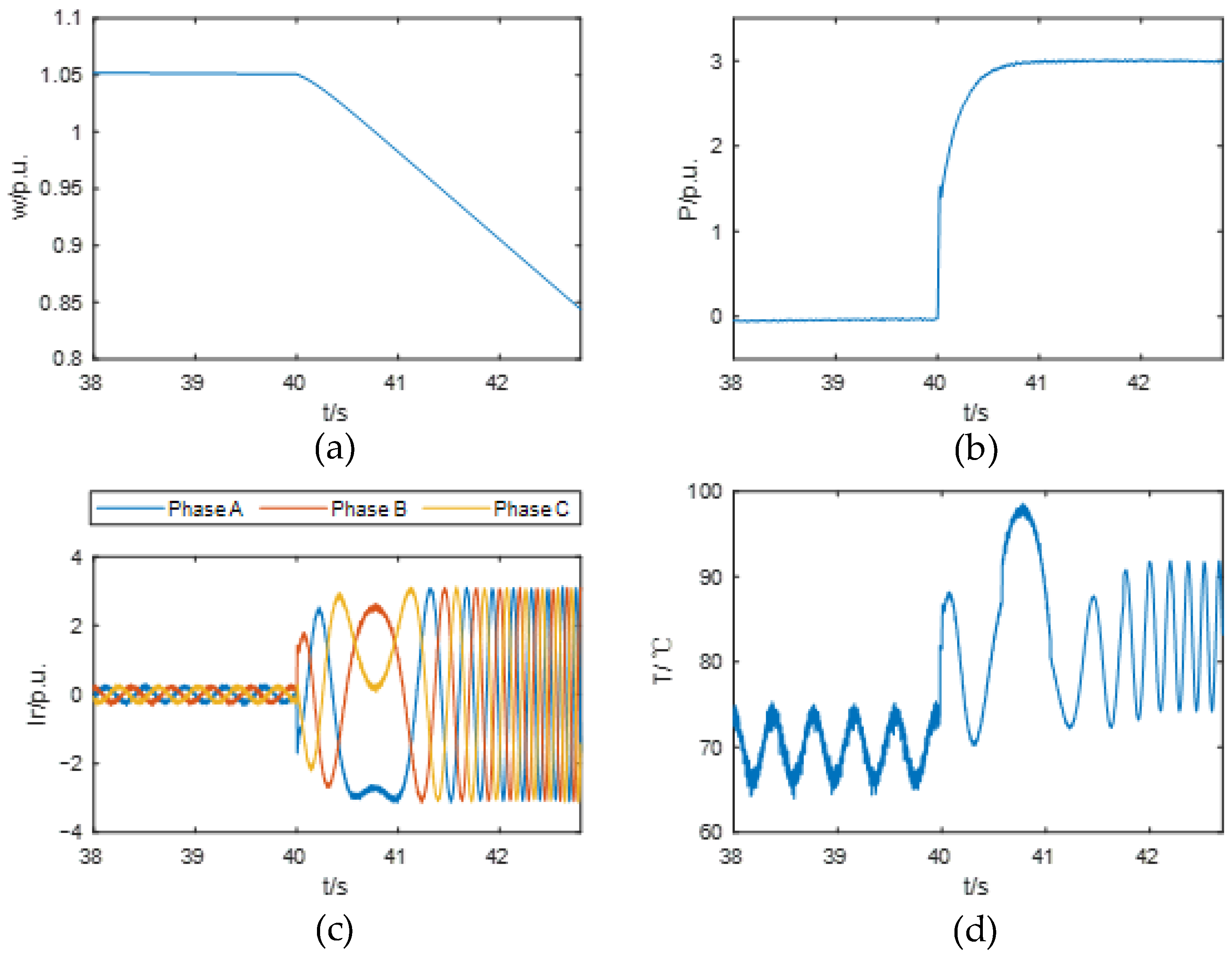
To further study the effect of different levels of active support of HI-ES-SC on junction temperature, active power outputs of HI-ES-SC are set to 1.0, 1.5, 2.0, 2.5, and 3.0 p.u. until speed decreases from 1.05 p.u. to 0.85 p.u. Maximum junction temperature and active power output duration are shown in Figure 12, Figure 13, Figure 14 and Figure 15. As the active output to the grid increases, the increase in current flowing through the converter causes an increase in the junction temperature maximum. However, increasing the output active power significantly shortens the speed reduction process from 8 s to 2.8 s. This reduction in duration decreases heat accumulation time. As a result, the maximum junction temperature rises only marginally: from 81.69 °C to 83.46 °C, 85.23 °C, 92.74 °C, and 98.50 °C.
Figure 16 shows the curves of speed, active and rotor currents, and junction temperature of the converter when the HI-ES-SC continuously outputs 1.0 p.u. of reactive power. Keeping the rotational speed constant, the HI-ES-SC starts to continuously output 1.0 p.u. reactive power at 40 s. Compared with the rotor current and junction temperature curves in Figure 11, during the reactive power output period, the HI-ES-SC rotational speed is maintained constant, and the frequency of rotor current and junction temperature fluctuation changes less. During 40 s~43 s, compared with the active output, the transition process of reactive power output is smoother, and there is no significant junction temperature peak. After 44 s, the maximum and minimum junction temperatures of the HI-ES-SC active and reactive outputs are relatively close to each other. This can be obtained, HI-ES-SC output reactive power can maintain a relatively constant speed, and the impact on the junction temperature is less than the same value of the active output under the working conditions.
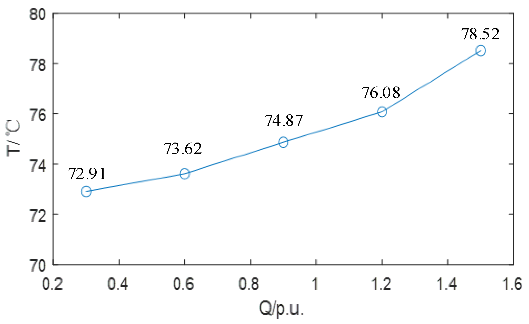
Figure 17 shows the effect of different degrees of reactive power support of HI-ES-SC on the junction temperature. Keeping the HI-ES-SC speed at 1.05 p.u. makes the HI-ES-SC active output 0.3 p.u., 0.6 p.u., 0.9 p.u., 1.2 p.u., and 1.5 p.u. for 8 s, respectively. As the reactive power output increases, the maximum value of junction temperature and fluctuation of the converter increase. From Formula (5), it can be seen that the increase in reactive power output from the doubly fed motor of the HI-ES-SC causes an increase in reactive current, and the maximum value of junction temperature rises. Compared with Figure 11, Figure 12, Figure 13, Figure 14 and Figure 15, the maximum value of junction temperature changes with the increase in reactive power by a small amount because the process of rotor current change does not involve speed change during the process of reactive power output from the HI-ES-SC, and the transition time is short.

5. Conclusions

This paper focuses on the machine-side three-level converter of HI-ES-SC, establishes an electro-thermal coupling model for the converter, and analyzes the evolution of electrical quantities and temperature rise patterns of HI-ES-SC during active and reactive power outputs through Simulink-PLECS co-simulation. Main conclusions are as follows:
  • The proposed model demonstrates low sensitivity to parameter variations and achieves high simulation accuracy across multiple time scales. Although the thermal resistance and thermal capacitance parameters exhibit errors in the range of approximately 2.8% to 9.6%, experimental results indicate a simulation deviation of about 1.6% in the single switching test. Under a prolonged 3 h test at rotor currents of 3.5 kA and 4 kA, the simulation deviations are approximately 0.5% and 3.3%, respectively. The model performs consistently well across different studies and parameter sets, demonstrating its strong potential to serve as a theoretical basis for device parameter selection in practical converter design.
  • When the HI-ES-SC provides high-level active power support (e.g., up to 3.0 p.u.), the junction temperature rises significantly as the rotor speed crosses the synchronous speed. This phenomenon is primarily caused by thermal accumulation effects in the converter during low-frequency operation. Under 3.0 p.u. active power support, the peak junction temperature reaches 98.50 °C.
  • In contrast, reactive power support has a minor impact on the junction temperature variation in the converter. Since the HI-ES-SC can maintain a relatively constant speed during reactive power output, it avoids low-frequency operation of the converter, which is the main contributor to significant temperature rise. Under 1.5 p.u. reactive power support, the peak junction temperature is only 78.52 °C.
However, the proposed model still has certain limitations, which will be addressed in our future work regarding the following aspects:
  • It is applicable only to air-cooled heat sinks. For water-cooled systems, modeling and analysis must account for specific thermal dissipation structures.
  • Further research is needed to investigate the impact of more factors on the accuracy of the model.

Author Contributions

Conceptualization, J.O.; methodology, J.O.; software, Y.L.; validation, Y.L.; formal analysis, Y.L.; investigation, J.O.; resources, Z.Y.; data curation, Y.D.; writing—original draft preparation, Y.L.; writing—review and editing, Y.L.; visualization, Z.Y.; supervision, J.O.; project administration, J.O.; funding acquisition, Y.D. All authors have read and agreed to the published version of the manuscript.

Funding

This research was funded by the National Key Research and Development Program, Ministry of Industry and Information Technology of the People’s Republic of China, number: 2023YFB2406800.

Data Availability Statement

Data are contained within the article.

Conflicts of Interest

The author declares no conflicts of interest. The funders had no role in the design of the study; in the collection, analyses, or interpretation of data; in the writing of the manuscript; or in the decision to publish the results.

Abbreviations

The following abbreviations are used in this manuscript:
HI-ES-SCHigh-Inertia Energy Storage Synchronous Condensers
UHVDCUltra-High Voltage Direct Current
NPCMid-Point Clamped
ANPCActive Mid-Point Clamped
IGCTIntegrated Gate-Commutated Thyristor
IGBTInsulated Gate Bipolar Transistors
FEMFinite Element Model
TSEPTemperature-Sensitive Electrical Parameter

References

  1. Ouyang, J.; Pan, X.; Ye, J.; Xiao, C.; Diao, Y.; Zhang, Q. An Improved Prediction Method of Subsequent Commutation Failure of an LCC-HVDC Considering Sequential Control Response. Prot. Control. Mod. Power Syst. 2023, 8, 1–11. [Google Scholar] [CrossRef]
  2. Ouyang, J.; Chen, J.; Li, A.; Chen, Y.; Xiao, C. Fault Ride-Through Control Method for VSC-HVDC Balancing between DC Voltage Security and Reactive Power Support. Trans. China Electrotech. Soc. 2024, 39, 6129–6144. [Google Scholar] [CrossRef]
  3. Muniappan, M. A Comprehensive Review of DC Fault Protection Methods in HVDC Transmission Systems. Prot. Control. Mod. Power Syst. 2021, 6, 1–20. [Google Scholar] [CrossRef]
  4. Xu, G.; Wang, L.; Li, Z.; Li, Z.; Zhao, H.; Zhan, Y.; Zhang, Y. Improvement of Reactive Power Consumption Ability for Dual-Excited Synchronous Condenser. IEEE Trans. Ind. Appl. 2024, 60, 6056. [Google Scholar] [CrossRef]
  5. Guo, Q.; Li, Z. Summarization of Synchronous Condenser Development. Proc. CSEE 2023, 43, 6050–6064. [Google Scholar]
  6. Lee, I.; Lee, K. Junction Temperature Estimation of SiC MOSFETs in Three-Level NPC Inverters. J. Electr. Eng. Technol. 2024, 19, 1607–1617. [Google Scholar] [CrossRef]
  7. Li, Z.; Jiang, W.; Wang, Y.; Li, W.; Li, C.; Xian, Z. Key Technical Parameters and Optimal Design of New Types of Large Capacity Synchronous Condenser. Large Electr. Mach. Hydraul. Turbine 2017, 4, 15–22. [Google Scholar]
  8. Zhang, B.; Wang, Z.; Gu, M. An Improved Si/SiC Hybrid Three-Level ANPC Inverter with Optimized Thermal Distribution-Based Modulation Scheme. In Proceedings of the 27th International Conference on Electrical Machines and Systems, Fukuoka, Japan, 26–29 November 2024; pp. 1012–1017. [Google Scholar]
  9. Woldegiorgis, D.; Mantooth, H. Precise Electro-thermal Power Loss Model of a Three-level ANPC Inverter with Hybrid Si/SiC Switches. Chin. J. Electr. Eng. 2022, 8, 76–89. [Google Scholar] [CrossRef]
  10. Zhang, Y.; Zhou, J.; Zhou, S.; Li, S.; Wen, Z.; Ji, Y. Loss Analysis and Junction Temperature Prediction for Modular Multilevel Converters. In Proceedings of the 9th International Conference on Power And Renewable Energy, Guangzhou, China, 20–23 September 2024; pp. 156–161. [Google Scholar] [CrossRef]
  11. Musarrant, M.N.; Islam, M.R.; Muttaqi, K.; Sutanto, D.; Rahman, M.A. Improving the Thermal Performance of Rotor-Side Converter of Doubly Fed Induction Generator Wind Turbine While Operating Around Synchronous Speed. IEEE J. Emerg. Sel. Top. Ind. Electron. 2022, 3, 298–307. [Google Scholar] [CrossRef]
  12. Charalambous, A.; Hadjidemetriou, L.; Polycarpou, M.M. Junction Temperature Control for Lifetime Extension of Multi-Functional Photovoltaic Inverters. IEEE Trans. Ind. Appl. 2024, 60, 4125–4137. [Google Scholar] [CrossRef]
  13. Ding, S.; Jiang, X.; Zhu, M.; Liu, W. Starting and Steady Temperature Rise Investigation for Permanent Magnet Synchronous Motor Based on Lumped-Parameter Thermal-Network. Electr. Mach. Control. 2020, 24, 143–150. [Google Scholar] [CrossRef]
  14. Xu, G.; Hu, P.; Li, Z.; Zhan, Y.; Zhao, H. Influence of Different Steady State Conditions on Transient Temperature Rise of Synchronous Condenser After Single-phase Short-circuit. Proc. CSEE 2024, 44, 1587–1597. [Google Scholar] [CrossRef]
  15. Liu, J.; Liu, Y.; Wen, C.; Qiu, D.; Guo, T.; Li, J. A Real-Time Junction Temperature Evaluation Method Based on the Reduction Thermal Model for IGBT Module of Traction Converter. IEEE Trans. Transp. Electrif. 2025, 11, 9319–9331. [Google Scholar] [CrossRef]
  16. Wu, J.; Wei, Y.; Wu, Y.; Wang, Z.; Li, X.; Wei, X. Research on Junction Temperature Smooth Control of SiC MOSFET Based on Body Diode Conduction Loss Adjustment. Energies 2024, 17, 6175. [Google Scholar] [CrossRef]
  17. Zhang, Q.; Zhang, P. A Junction Temperature Smoothing Control Method for SiC MOSFETs Based on the Gate Driving Signal Delay. IEEE Trans. Ind. Electron. 2023, 71, 3122–3132. [Google Scholar] [CrossRef]
  18. Fu, X.; Jin, M.; Huang, Y.; Du, J.; Wei, K. On-Line Junction Temperature Identification of Converter Power Devices. J. Phys. Conf. Ser. 2025, 2840, 012026. [Google Scholar] [CrossRef]
  19. Cho, S.; Song, S. A Study on the Power Loss of the High Voltage IGBT for Voltage Type HVDC MMC System. J. Korean Inst. Illum. Electr. Install. Eng. 2021, 35, 31–35. [Google Scholar] [CrossRef]
  20. Wang, Y.; Liang, Z.; Jin, B.; Pang, J. A Thermal Impedance Model for IGBT Modules Considering the Nonlinear Thermal Characteristics of Chips and Ceramic Materials. Electronics 2024, 13, 4465. [Google Scholar] [CrossRef]
  21. Zhang, X.; Mu, W.; Lv, C.; Shi, M.; Yu, X.; Wu, K.; Li, J. A Thermal Network Model for Monitoring IGBT Chip Solder Degradation Based on Feedback PI Control. Microelectron. Reliab. 2022, 138, 114617. [Google Scholar] [CrossRef]
  22. Xu, C.; Zhao, B.; Zhang, X.; Chen, Z.; Liu, J.; Zhou, W. Full-Time Junction Temperature Extraction of IGCT Based on Electrothermal Model and TSEP Method for High-Power Applications. IEEE Trans. Ind. Electron. 2021, 68, 47–58. [Google Scholar] [CrossRef]
  23. Yan, X.; Yu, Z.; Qu, L.; Gan, Z.; Huang, Y.; Feng, J. Electro-Thermo-Mechanical Analysis and Modeling of High-Power Intergrated Gate Commutated Thyristors. IEEE Trans. Power Electron. 2024, 39, 6654–6663. [Google Scholar] [CrossRef]
  24. Zhu, H.; Wu, J.; Wang, P.; Liu, J.; Chen, Z. Study on Accelerated Aging Test Topology for High Power Semiconductor IGCT Devices Targeting MMC Applications. Proc. CSEE. 2025, 45, 266–277. [Google Scholar] [CrossRef]
  25. Okilly, A.; Harmony, P.; Kim, C.; Kim, D.; Beak, J. Estimation of Peak Junction Hotspot Temperature in Three-Level TNPC-IGBT Modules for Traction Inverters Through Chip-Level Modeling and Experimental Validation. Energies 2025, 18, 3829. [Google Scholar] [CrossRef]
  26. Ouyang, J.; Yu, J.; Long, X.; Diao, Y.; Wang, J. Coordination Control Method to Block Cascading Failure of a Renewable Generation Power System Under Line Dynamic Security. Prot. Control. Mod. Power Syst. 2023, 8, 12. [Google Scholar] [CrossRef]
  27. Liu, H.; Xiang, C.; Du, J.; Zhang, X. Multi-Objective Cooperative Control of a Junction-Temperature-Orientated Three-Level Traction Converter. Transp. Saf. Environ. 2025, 7, tdaf017. [Google Scholar] [CrossRef]
  28. Guo, C.; Zhu, Y.; Tong, L. Junction Temperature Prediction for Multi-Chip IGBT Modules Based on An Improved 3D Thermal Network Model and Experimental Results. Results Eng. 2025, 27, 106072. [Google Scholar] [CrossRef]
  29. ABB. IGCT 5SHX 26L4503 datasheet, Doc. No. 5SYA 1230-01; ABB: Lenzburg, Switzerland, 2020; Available online: https://www.5scomponents.com/PDF/5SHX-26L4503_5SYA1230-01Feb-02.pdf (accessed on 1 September 2025).
  30. Hu, J. An H∞ Observer-based 3-D Thermal Monitoring Method for Multi-chip IGBT Modules with Robustness to Model Parameter and Power Loss Uncertainty. Prot. Control. Mod. Power Syst. 2025, 10, 125–145. [Google Scholar] [CrossRef]
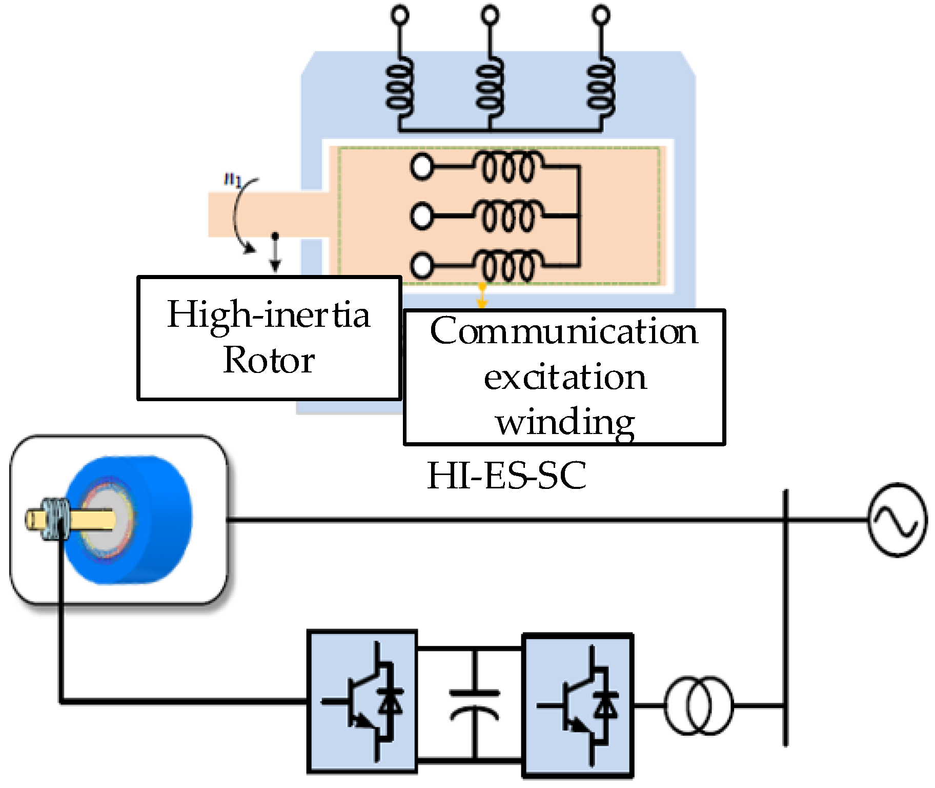
Figure 1. Structure of HI-ES-SC.
Electricity 06 00053 g001
Figure 2. Topology of converter for HI-ES-SC: (a) grid-side converter; (b) machine-side converter.
Electricity 06 00053 g002
Figure 3. Thermal network model of IGCT.
Electricity 06 00053 g003
Figure 4. Thermal network model of diode.
Electricity 06 00053 g004
Figure 5. Thermal network model of converter.
Electricity 06 00053 g005
Figure 6. IGCT nonlinear iterative temperature calculation method.
Electricity 06 00053 g006
Figure 7. Comparison of junction temperature curves for single switching test.
Electricity 06 00053 g007
Figure 8. Temperatures at peak and maximum deviation in the proposed model and FEM under different wind speeds.
Electricity 06 00053 g008
Figure 9. Comparison of junction temperature curves for single switching test with measured data.
Electricity 06 00053 g009
Figure 10. Converter electro-thermal coupling co-simulation model.
Electricity 06 00053 g010
Figure 11. Key characteristics of HI-ES-SC at 1.0 p.u. active power output: (a) rotational speed; (b) active power; (c) rotor current; (d) junction temperature.
Electricity 06 00053 g011
Figure 12. Key characteristics of HI-ES-SC at 1.5 p.u. active power output: (a) rotational speed; (b) active power; (c) rotor current; (d) junction temperature.
Electricity 06 00053 g012
Figure 13. Key characteristics of HI-ES-SC at 2.0 p.u. active power output: (a) rotational speed; (b) active power; (c) rotor current; (d) junction temperature.
Electricity 06 00053 g013
Figure 14. Key characteristics of HI-ES-SC at 2.5 p.u. active power output: (a) rotational speed; (b) active power; (c) rotor current; (d) junction temperature.
Electricity 06 00053 g014
Figure 15. Key characteristics of HI-ES-SC at 3.0 p.u. active power output: (a) rotational speed; (b) active power; (c) rotor current; (d) junction temperature.
Electricity 06 00053 g015
Figure 16. Key characteristics of HI-ES-SC at 1.0 p.u. reactive power output: (a) rotational speed; (b) active power; (c) rotor current; (d) junction temperature.
Electricity 06 00053 g016
Figure 17. Maximum converter junction temperature under different reactive power outputs.
Electricity 06 00053 g017
Table 1. IGBT and IGCT’s structures and characteristics.
DeviceIGBTIGCT
Chip structureSmall-sized chips with complex cellsWhole crystal chip with relatively simple cell structure
Package formComplex multi chip parallel packagingSimple and reliable whole wafer packaging
Production costComplex structure and high costSimple structure and low cost
Switching frequencyHigh, above several kilohertzLower, several hundred hertz
Shutdown capabilitystrongstronger
Dynamic tolerancedi/dt is controllable through drivingdi/dt controlled by loop inductance
Working lossHigh tolerance of dv/d under black startHigh tolerance of dw/dt under black start
Drive powerHigh opening and conduction lossesLow opening and conduction losses
Capacity characteristicsHigh shutdown loss after low-frequency optimizationHigh shutdown loss
Security featureslowerSignificant decrease at high and low frequencies
Table 2. On-duty ratio of switching device.
Switch StateVoltage Level StateDuty CycleConducting Device of Current Switching Path 1Conducting Device of Current Switching Path 2
Ir > 0Ir < 0Ir > 0Ir < 0
P-O level change1/2Udcm sin(ωit + φ)VT1, VT2VD1, VD2VT1, VT2VT6, VD3
01 − msin(ωit + φ)VD5, VT2VT5, VD2VD1, VD2VT3, VD6
O-N level change01 + msin(ωit + φ)VD5, VT2VD6, VT3VD3, VT6VD2, VT5
−1/2Udcm sin(ωit + φ)VD3, VD4VT4, VT3VD3, VD4VT3, VT4
Table 3. Parameters of the IGCT thermal model.
IGCTSi(IGCT Wafer)Al(Electrode) *Mo(Mo Piece)Cu(Case Bolock)
Material
Parameter
C (J/gK)0.70.760.250.39
ρ (g/cm3)2.333.9710.28.96
λ (W/cmK)1.480.361.384.01
Cathode
Parameter
D (cm)8.98.98.910.16
A (cm2)62.2162.2162.2181.07
L (cm)0.050.00120.251.015
R (K/W)0.000544.47 × 10−50.00290.0031
C (J/K)5.070.18839.66283.86
Anode
Parameter
D (cm)8.9/8.99.5
A (cm2)62.21/62.2170.88
L (cm)0.025/0.251.015
R (K/W)0.0003/0.0030.0036
C (J/K)2.54/39.66248.18
* there is no anode Al electrode in IGCT.
Table 4. Parameters of the RE.
ParameterValueParameterValue
tb13.7 mms5.6 mm
kAl255 W/(m K) ρ 1.0926 kg/m3
Bcond1.312 × 105 mm2 μ 1.961 × 10⁻⁵ kg/ms
η 0.89 P r 0.7124
kf0.0277 W/(m K) l w 76 mm
Table 5. Calculated RC parameters of the three models.
RC
Parameters
Model Based on FEMLinear Thermal ModelError of Linear Thermal ModelModel Proposed in This PaperError of the Model Proposed
RSi
(K/W)
5.74 × 10−41.06 × 10−3+84.67%5.83 × 10⁻⁴+1.57%
RMo
(K/W)
3.02 × 10−33.42 × 10−3+13.24%3.31 × 10⁻³+9.60%
RAl
(K/W)
4.65 × 10−56.20 × 10−5+33.33%4.91 × 10⁻⁵+5.59%
RCu
(K/W)
3.28 × 10−34.49 × 10−3+36.89%3.40 × 10⁻³+3.66%
CSi
(J/K)
5.905.23−11.36%5.62−4.75%
CMo
(J/K)
45.2342.97−5.00%42.26−6.57%
CAl
(J/K)
0.2280.206−9.65%0.219−3.95%
CCu
(J/K)
311.24289.06−7.13%302.45−2.82%
Table 6. Comparison of junction temperature with different Ir.
UDCIrJunction Temperature (Proposed Method)Junction Temperature (Experiment)
2.5 kV3.5 kA80.7 °C81.1 °C
4 kA92.3 °C95.5 °C
These results confirm that the proposed method maintains high accuracy under various operating conditions, in both short-term switching tests and long-term junction temperature evaluations.
Table 7. Parameters of the co-simulation model.
ParameterValueParameterValue
Solver choiceFixed-step, ode3Stator resistance0.074 Ω
Signal-exchange rate115,200Total stator leakage inductance6.11 mH
Rated capacity11.11 MVAExcitation inductance234.93 mH
Rated stator voltage10.5 kVRotor resistance0.0275 Ω
Rated rotor voltage3.3 kVTotal rotor leakage inductance6.4 mH
Pole-pair number1Stator/Rotor turns ratio0.6
No-load rated rotational speed3150 r/minDC bus voltage7000 V
Inertia time constant20.3 sDC bus capacitance30 mF
Rated slew rate±0.2%Inlet reactor inductance0.4 mH
Maximum slew rate3.5 kVInlet reactor resistance0.00298 Ω
Disclaimer/Publisher’s Note: The statements, opinions and data contained in all publications are solely those of the individual author(s) and contributor(s) and not of MDPI and/or the editor(s). MDPI and/or the editor(s) disclaim responsibility for any injury to people or property resulting from any ideas, methods, instructions or products referred to in the content.