Article

Controller Hardware-in-the-Loop Validation of a DSP-Controlled Grid-Tied Inverter Using Impedance and Time-Domain Approaches

by
Leonardo Casey Hidalgo Monsivais
1,
Yuniel León Ruiz
1,
Julio Cesar Hernández Ramírez
1,
Nancy Visairo-Cruz
1,
Juan Segundo-Ramírez
1,* and
Emilio Barocio
2,*
1
Center for Research and Graduate Studies, Universidad Autónoma de San Luis Potosí, San Luis Potosi 78290, Mexico
2
Graduate Program in Electrical Engineering, Universidad de Guadalajara, Guadalajara 44430, Mexico
*
Authors to whom correspondence should be addressed.
Electricity 2025, 6(3), 52; https://doi.org/10.3390/electricity6030052
Submission received: 10 July 2025 / Revised: 21 August 2025 / Accepted: 2 September 2025 / Published: 6 September 2025

Abstract

In this work, a controller hardware-in-the-loop (CHIL) simulation of a grid-connected three-phase inverter equipped with an LCL filter is implemented using a real-time digital simulator (RTDS) as the plant and a digital signal processor (DSP) as the control hardware. This work identifies and discusses the critical aspects of the CHIL implementation process, emphasizing the relevance of the control delays that arise from sampling, computation, and pulse width modulation (PWM), which also adversely affect system stability, accuracy, and performance. Time and frequency domains are used to validate the modeling of the system, either to represent large-signal or small-signal models. This work shows multiple representations of the system under study: the fundamental frequency model, the switched model, and the switched model controlled by the DSP, are used to validate the nonlinear model, whereas the impedance-based modeling is followed to validate the linear representation. The results demonstrate a strong correlation among the models, confirming that the delay effects are accurately captured in the different simulation approaches. This comparison provides valuable insights into configuration practices that improve the fidelity of CHIL-based validation and supports impedance-based stability analysis in power electronic systems. The findings are particularly relevant for wideband modeling and real-time studies in electromagnetic transient analysis.

1. Introduction

Increasing integration of electronic devices within power grids has posed novel challenges concerning system stability. A significant emerging concern arises from the uncontrolled surplus energy in elements of power electronics-based systems, which manifests in rapid oscillations of stored energy between electric and magnetic fields [1]. These oscillations lead to swift fluctuations in electrical and control variables. This phenomenon is particularly pronounced in grids that incorporate controlled power electronics converters. The modeling and simulation of these systems is indispensable for the identification, evaluation, and analysis of such phenomena. Hence, it is imperative to execute these simulations with precision, incorporating the necessary parameters, controls, and elements. Typically, dynamic simulations are conducted to examine stability phenomena, including transient, voltage, and frequency stability. Control and protection applications can also be evaluated in specific simulation environments to better understand primary system behaviour. However, the complete effects of hardware implementation are not fully considered in offline simulations. This is especially true for power electronic converters, controls, and protection mechanisms that have a fast response. Consequently, the control hardware must be evaluated along with the simulation model of the system, particularly in advanced stages of test development. These simulation approaches, combining control hardware and real-time simulators, are known as controller hardware-in-the-loop simulations. Despite the advantages that CHIL simulations offer, such as a more realistic test environment, detailed models, safe operative conditions, and automation and repetitiveness of tests, there are still several challenges behind the successful implementation of this approach.
Various studies have implemented CHIL in different contexts. In [2], a passive method for detecting islanding based on the phase angle of overlapping negative sequence components is validated. Although the detection method is implemented in a dSPACE 1104 and the RTDS is used to develop a benchmark IEEE-34 bus network, none of the control systems of the generation units is dumped into an external hardware, and consequently the impact of the pulse width modulation strategy on the power system is not documented. The authors in [3] designed a robust controller to cope with network impedance variations and evaluates it in a CHIL environment. In this environment, the plant consisting of a high-voltage direct current (HVDC) link and a modular multilevel converter (MMC) was modeled in an RTDS and coupled to a controller implemented in a Xilinx Zynq XC7Z030-3FBG676E DSP/FPGA. Validation was performed by analyzing the system admittance. However, the impact of switching delays was not evaluated, nor was a comparison between the analytical model and the results obtained in CHIL presented. The work proposed in [4] developed a real-time co-simulation platform for grid-forming storage system controllers. This advanced simulation ecosystem allows for rapid control testing of an experimental test bench using an RTDS and an FPGA controller. Despite using powerful tools in the context of a CHIL setup, the proposal fails to provide guidelines for the control hardware implementation to mitigate instability caused by the inherent delays of the feedback loop. The work described in [5] proposes a comprehensive validation framework for power electronics systems that integrates SIL, HIL, CHIL, PHIL, and RCP. The framework is exemplified by a two-stage cascade conversion plant: a boost stage that controls the maximum power extracted from the photovoltaic panel and an inverter stage under control in the synchronous d–q frame, which maintains the DC bus voltage constant and regulates the reactive power injected into the grid. The methodology includes offline simulations, real-time simulations, and finally, a CHIL simulation. The real-time simulation is run entirely on the F28379D DSP; the CHIL is implemented on an Opal-RT OP-4510, separating the power and control circuits into different processors and considering the communication delays between them. The latencies in both configurations are analyzed and the resulting signals are compared. However, although aspects of the delays and the implementation of the PWM are discussed, the study does not address guidelines for external control hardware or evaluate the impact of these delays on controller performance. Finally, ref. [6] proposes a real-time testing method for digital power electronics controllers. The platform implements real-time simulation in an RTDS, coupled to an external controller based on a TI TMS320C28x DSP. Different representative cases are evaluated, including a buck type DC-DC converter and a DC-AC converter, and the duty cycle, the plant structure within the RTDS, and the control algorithm executed in the DSP are discussed. It also briefly addresses the switching frequency limitation imposed by the plant integration step in the RTDS and compares the results obtained between the configurations. Although it demonstrates the feasibility of the CHIL implementation, the study does not present comparisons with analytical models or experimental results.
This article addresses challenges in simulating a grid-connected three-phase inverter with an LCL filter. It uses a real-time digital simulator (RTDS) to model the plant and a digital signal processor (DSP) for control, and provides insights into the process of closing the loop via the control hardware. In the experience of the authors, these observations are valuable for less-experienced users and beginners as they can help save time in the debugging stages of the testing process. Preliminary results, figures, and models presented in the article were initially developed as part of the first author’s master’s thesis [7]. The remainder of this article is organized as follows. Section 2 discusses the main features of CHIL simulation. Section 3 presents the inverter model used in the real-time simulator, along with the PI control and phase-locked loop (PLL) used to manage power flow. Section 4 outlines a methodology for implementing CHIL. Section 5 discusses the test results and compares them with the mathematical model.

2. Introduction to Control Hardware-in-the-Loop Simulation

Hardware-in-the-loop (HIL) simulations involve integrating physical components into the simulation environment, rather than relying solely on digital mathematical models. When the controller is the physical component in the HIL setup, this configuration is referred to as controller hardware-in-the-loop (CHIL) [8,9]. CHIL simulations do not imply power transferred between the real-time simulation and the hardware. The interchange of signals between the digitally modeled plant and the hardware is performed only for communication protocols or low-power signals (voltage or currents). This method is generally used to test newly developed controllers. Figure 1 illustrates a basic implementation of CHIL, in which the power electronic converter is represented within the real-time simulator environment, while the controller interacts through the simulator’s interfaces. These concepts are better explained in [10].

3. Modeling of Three-Phase Inverter and Control

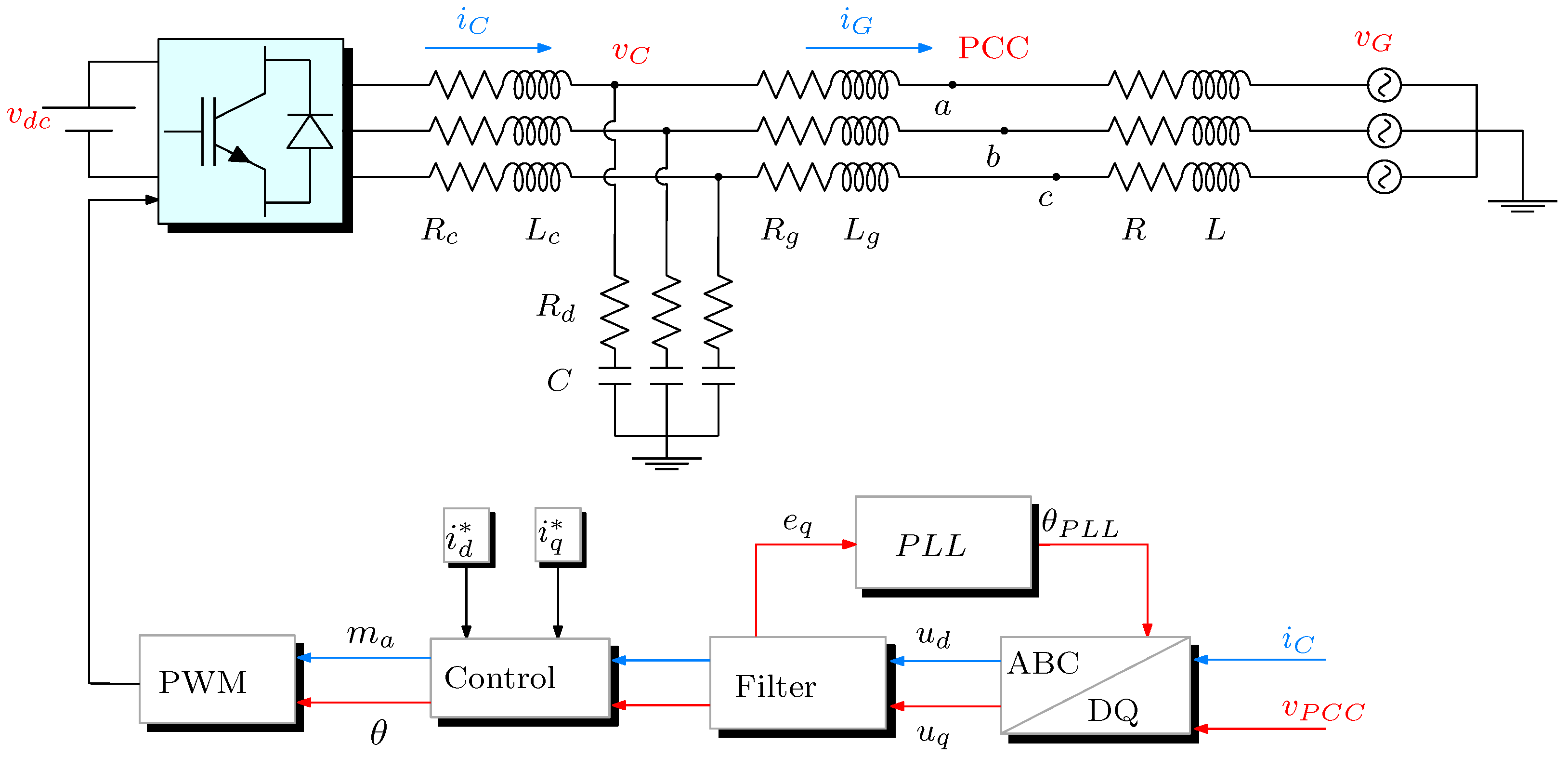
This section presents the test system used to validate and show the CHIL simulation approach. It briefly mentions the elements involved in the simulation, the plant, the control laws, and the synchronization control in the time domain. Moreover, a linear model of the system around the steady-state operating point is presented. For this purpose, the impedance model is derived in the d q framework by considering only the positive sequence in the frequency domain, assuming a balanced system.

3.1. Three-Phase Grid-Connected Inverter

Figure 2 shows the control implementation diagram for the three-phase inverter. By expressing the current and voltage components in dq coordinates, the control strategy is simplified since it allows for setting independent current references for the d and q components.

3.2. Phase-Locked Loop

To implement the control in the dq reference frame, the transformation from abc to dq must be carried out. This transformation relies on the usage of the phase obtained from the phase-locked loop (PLL) as a reference frame. The PLL illustrated in Figure 3 is capable of obtaining the phase of a signal; in this way, the PLL acquires information from the electrical network, thus synchronizing the voltage and current signals between the converter and the electrical network.

3.3. Control Scheme

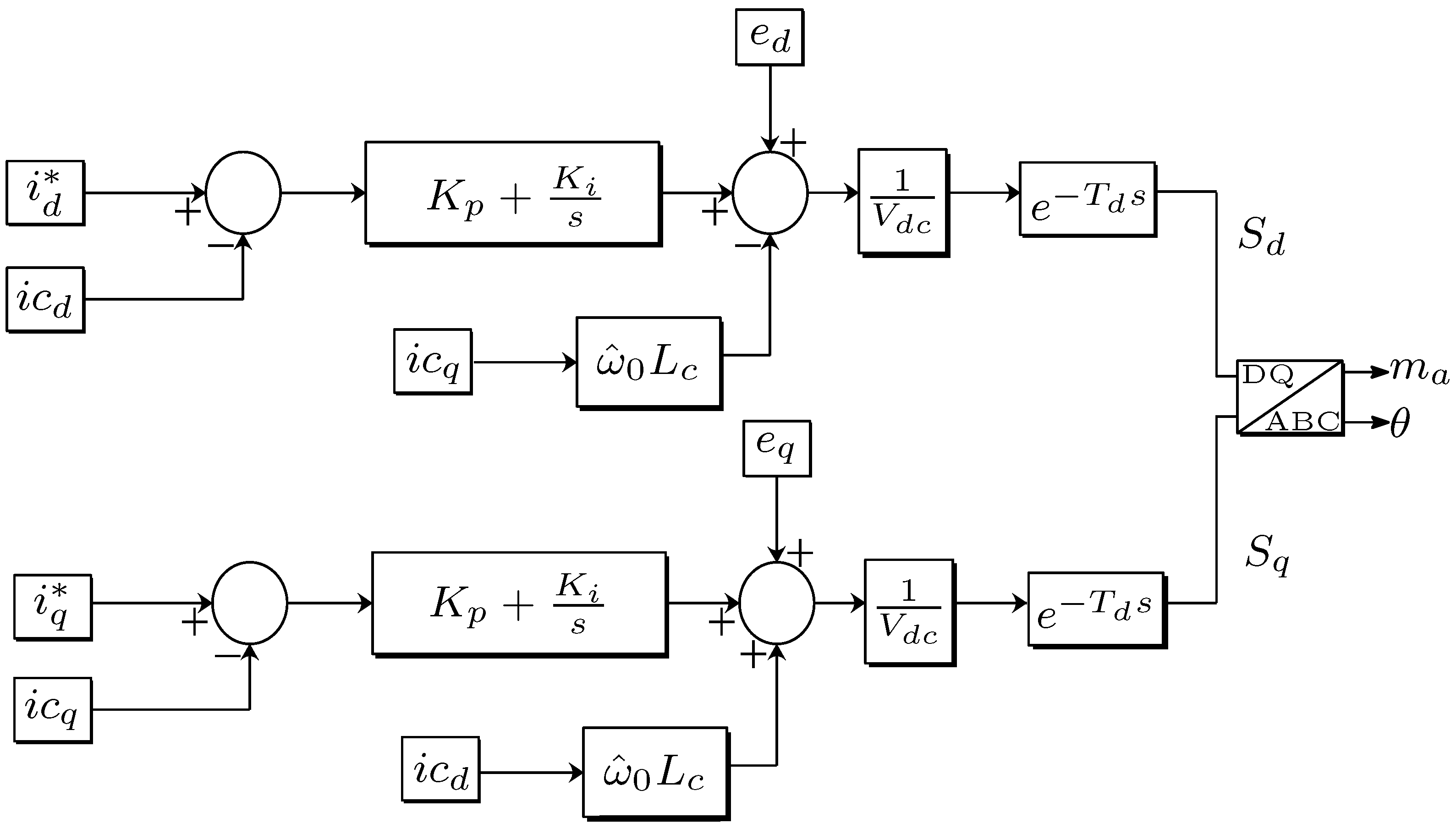
Currently, various control strategies are employed in voltage-source converters (VSCs), providing the flexibility to select the most suitable one based on system requirements. Some of these strategies regulate the grid voltage and frequency, and control the exchange of active and reactive power between the converter and the grid. In this study, a grid-following mode is adopted, which enables direct control of active and reactive power. The control scheme proposed in [11] is illustrated in Figure 4, which assumes ideal decoupling of the d and q components, allowing independent regulation of the current and voltage along each axis. In practice, however, some degree of coupling remains due to system dynamics and hardware limitations.

3.4. PI Controller Tuning

To calculate K p and K i , frequency response tuning is used, as it is a technique used in the design of controllers for control systems. It consists of adjusting the controller parameters so that the frequency response of the closed-loop system meets certain performance requirements, such as gain margin and phase margin [12]. Consider the following open-loop model:
L ( s ) = C ( s ) D ( s ) F ( s ) G ( s )
where C ( s ) = K p T n s + 1 T n s is the PI; D ( s ) = 1 1.5 T s w i t c h i n g s + 1 groups the effects of digitization as if it were 1.5 times the switching period ( T s w i t c h i n g ) of the PWM; F ( s ) = 1 τ s + 1 is the digital filter; and G ( s ) is the plant. Given the crossover frequency ω c ( r a d s ) and the desired phase margin (PM) in degrees, the following conditions apply:
  • Phase condition for calculating T n is
    PM = 180 + C + D + F + G
  • Module condition for calculating K p in ω c requires that L ( j ω c ) = 1 , i.e.,
    1 = C ( j ω c ) D ( j ω c ) F ( j ω c ) G ( j ω c )

3.5. Three-Phase Closed-Loop Inverter Model

The time-domain model of the three-phase closed-loop inverter used in this study is based on the approach presented in [13], where a generalized framework for n parallel inverters connected to the grid was developed. The closed-loop control law adopts the formulation proposed in [11]. The models detailed in [14] provide the basis for deriving the impedance model discussed in the following subsection. See Appendix A for the equations that characterize the closed-loop inverter dynamics.

3.6. Small-Signal Impedance Model

The 2 × 2 source-side impedance matrix of the test system shown in Figure 2, denoted by Z s ( s ) , is expressed in the Laplace domain as follows:
Z s ( s ) = I + RD + Y 1 Z 1 Z 1 G e 1 × RD + Y 1 I Z 1 G d
In the matrix Z s ( s ) , the diagonal elements Z s d d ( s ) and Z s q q ( s ) correspond to the impedances along the d- and q-axes, respectively. The off-diagonal terms Z s d q ( s ) and Z s q d ( s ) represent the cross-coupling between these axes. This matrix is arranged by
Z s ( s ) = Z s d d ( s ) Z s d q ( s ) Z s q d ( s ) Z s q q ( s )
The matrices involved in Equation (4) are briefly described below. Key components include the diagonal matrices C i , RD , G f f v , and G f f i , representing the PI current controller, damping resistor, voltage filter, and current filter, respectively. Variables with a subscript zero, x 0 , denote their corresponding steady-state values. Z is part of the filter impedance in the dq reference frame. The diagonal elements include R c and L c ω b s , while the off-diagonal terms capture the cross-coupling induced by L c .
C i = K p d q + K i d q s 0 0 K p d q + K i d q s
RD = R d 0 0 R d
G f f v = 1 τ f f v s + 1 0 0 1 τ f f v s + 1
G f f i = 1 τ f f i s + 1 0 0 1 τ f f i s + 1
Z = R c + L c ω b s L c L c R c + L c ω b s
Y represents the admittance of the filter capacitor, also expressed in dq coordinates. The diagonal elements contain the capacitive term C ω b s , while the off-diagonal elements account for the capacitive coupling:
Y = C ω b s C C C ω b s
Park’s transformation matrix T is used to transform the three-phase ( a b c ) system into the rotating d q reference frame:
T = cos ( δ ) sin ( δ ) sin ( δ ) cos ( δ )
G a models the dynamics associated with the PLL and the voltage filter. It incorporates the PLL gain G p l l , voltage filter gain G f f v , and the transformation matrices T and its time derivative T ˙ , evaluated at the operating point v P C C 0 .
G a = 1 ω b s G p l l G f f v T ˙ v P C C 0 1 ω b s G p l l G f f v T
G b captures the contribution of the voltage filter to the system, combining the filter gain G f f v with the effects of coordinate transformation and PLL dynamics via G a .
G b = G f f v T + T ˙ v P C C 0 G a
G c incorporates the current controller C i , the compensation gain G L c , the current filter G f f i , and the PLL-related dynamics.
G c = C i + G L c G f f i T ˙ I D Q 0 G a + G b
G d reflects the impact of the digital delay e T s s introduced by the switching frequency, as well as the dynamics of the current controller. The DC bus voltage V d c scales the overall gain.
G d = V d c T 1 e T s s V d c C i + G L c G f f i T
G e is a composite expression that aggregates several system effects, including delay, controller dynamics, and interactions with the network impedance ( RD + Y 1 ) .
G e = V d c T 1 e T s s V d c C i + G L c G f f i T RD + Y 1 1 + T 1 e T s s V d c G c + T ˙ 1 e d q 0 G a

4. Insights into DSP-Based Control Integration with RTDS

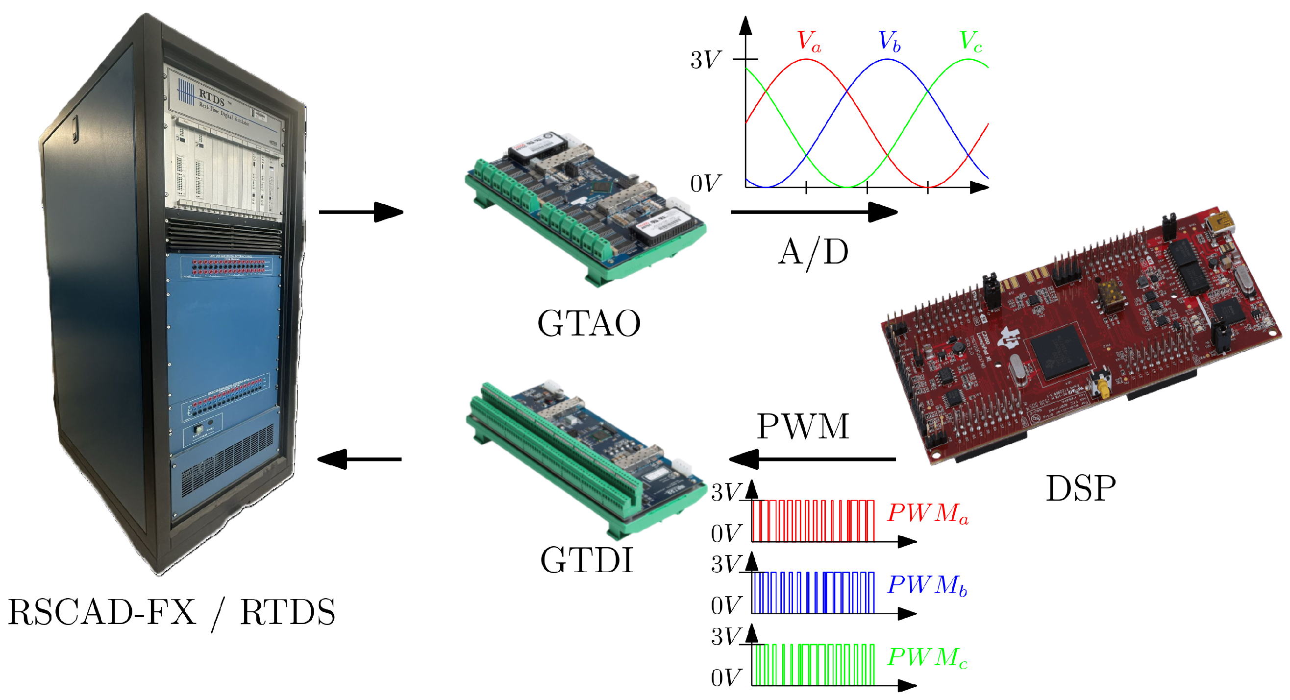
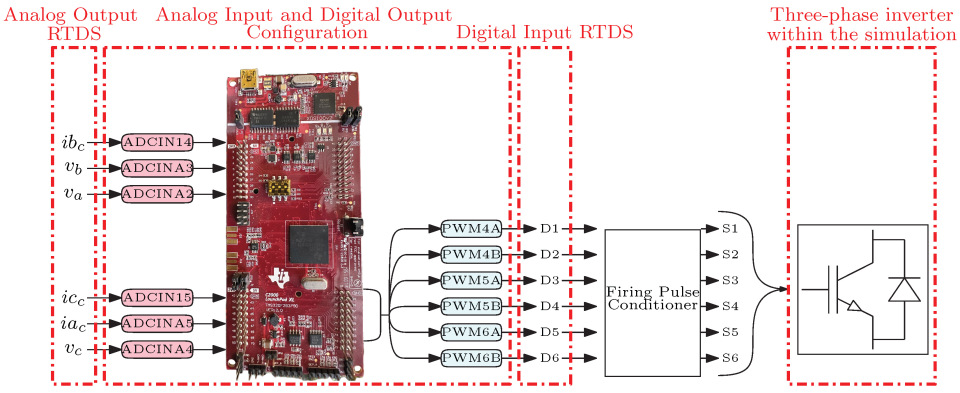
The implementation of CHIL allows the performance of the controller to be verified under realistic conditions prior to its practical application. In this context, the RTDS is used as the plant, while the DSP is the hardware responsible for controlling the inverter switching, as visualized in Figure 5.

4.1. Procedure

For a proper implementation of CHIL, the following steps are recommended:
  • Define the system to be controlled: Identify the system to be controlled and establish clear objectives.
  • Select system components: Choose necessary elements such as the real-time simulator and data processing board.
  • Configuring the simulation environment: Set up the simulator as a plant and configure all the necessary parameters.
  • Calibrate the inverter parameters: Adjust the three-phase inverter parameters within the simulation, including the gigabit transceiver digital output (GTAO) and the gigabit transceiver digital input (GTDI) settings.
  • Integrate hardware and software: Connect DSP to RTDS, ensuring correct signal transmission.
  • Perform initial tests: Perform preliminary tests to verify the correct operation and effectiveness of communication.
  • Execute the CHIL simulation: Conduct simulations under different operating conditions to evaluate controller performance.
  • Analyze results and adjust: Review the results obtained and make adjustments to the controller as necessary.
Following the above steps helps to avoid conflicts during CHIL implementation. Clearly defining the system to be controlled is fundamental; for instance, a three-phase inverter capable of transferring power to the grid with high efficiency is required, implementing control laws that adjust the current via proper switching of the inverter [15].

4.2. Timing and Digital Control Implementation

The selection of system components demands careful consideration of their distinct characteristics, particularly regarding delay and accuracy in the GTAO, GTDI, and DSP cards. For the GTAO card, a write delay of approximately 9.203 μ s is presented in the simulation, due to its interface with the simulator [16]. While these delays from data transfer cards are inherent and unavoidable, they must be accounted for in test design to avoid compromising result accuracy. Proper hardware and software integration is crucial. If signals from the simulation are not correctly scaled or exhibit offsets, control laws in the DSP will not execute properly, producing inconsistent PWM signals. To accurately capture each switching transition and avoid missing SPWM pulses, at least N time steps per switching period is required. Thus, the maximum admissible switching frequency is f sw , max = 1 N Δ t s . Using Δ t s = 1.5 μ s and N = 10 gives f sw , max = 1 10 × 1.5 μ s 66.7 kHz . However, the maximum recommended switching frequency for modeling voltage-source converters in RTDS is 3 kHz. Beyond this threshold, the RTDS model experiences significant power losses. In order to implement continuous-time control laws within the DSP, it is necessary to discretize them using appropriate techniques that ensure accurate real-time execution. The method selected due to its numerical stability is bilinear transformation. This method can be briefly summarized by the following rule: given a continuous-time transfer function H ( s ) , its discrete equivalent is obtained using H T ( z ) = H ( s ) with s = 2 T z 1 z + 1 , according to [12]. This transformation helps to convert continuous transfer functions into difference equations that the DSP executes at fixed sampling intervals. The sampling frequency ( f s ) must be chosen according to the processing capacity of the DSP. For example, if the maximum clock frequency of the device is 100 kHz and a sampling frequency of 150 kHz , the processor will not be able to perform the calculations in the time available, which will degrade the controller’s performance and may make it unstable. In order to efficiently couple the control loop implemented within the DSP with the real-time simulation in the RTDS, it is essential to apply two constraints:
  • Frequency coverage. The sampling frequency within the RTDS must be sufficiently small to capture the dynamics of the controller, i.e., if the closed-loop control bandwidth ( f B W ) is 100 Hz , the rule applies f s 10 f B W ; therefore, it is sufficient for the sampling period of the real-time simulation to be less than 1 ms [17].
  • Deterministic synchrony. The DSP sampling period must be an integer multiple of the RTDS time step. This will prevent fluctuations because it ensures that each control interruption coincides exactly with a moment in the simulation [18].
Open-loop testing is recommended for each component and can be structured into three cases:
  • Evaluate only real-time simulation, either by implementing the control within the RTDS or by using constant values for the variables needed to construct the PWM signal that controls the power flow.
  • Evaluate only the DSP, making sure that the control laws are properly executed with constant current values and verifying that the generated PWM signals are coherent.
  • Connect the DSP to the RTDS, but control the system only by means of a PWM with predefined variables. This allows us to verify that the results obtained in the simulation are correct and to validate that each component is properly configured.
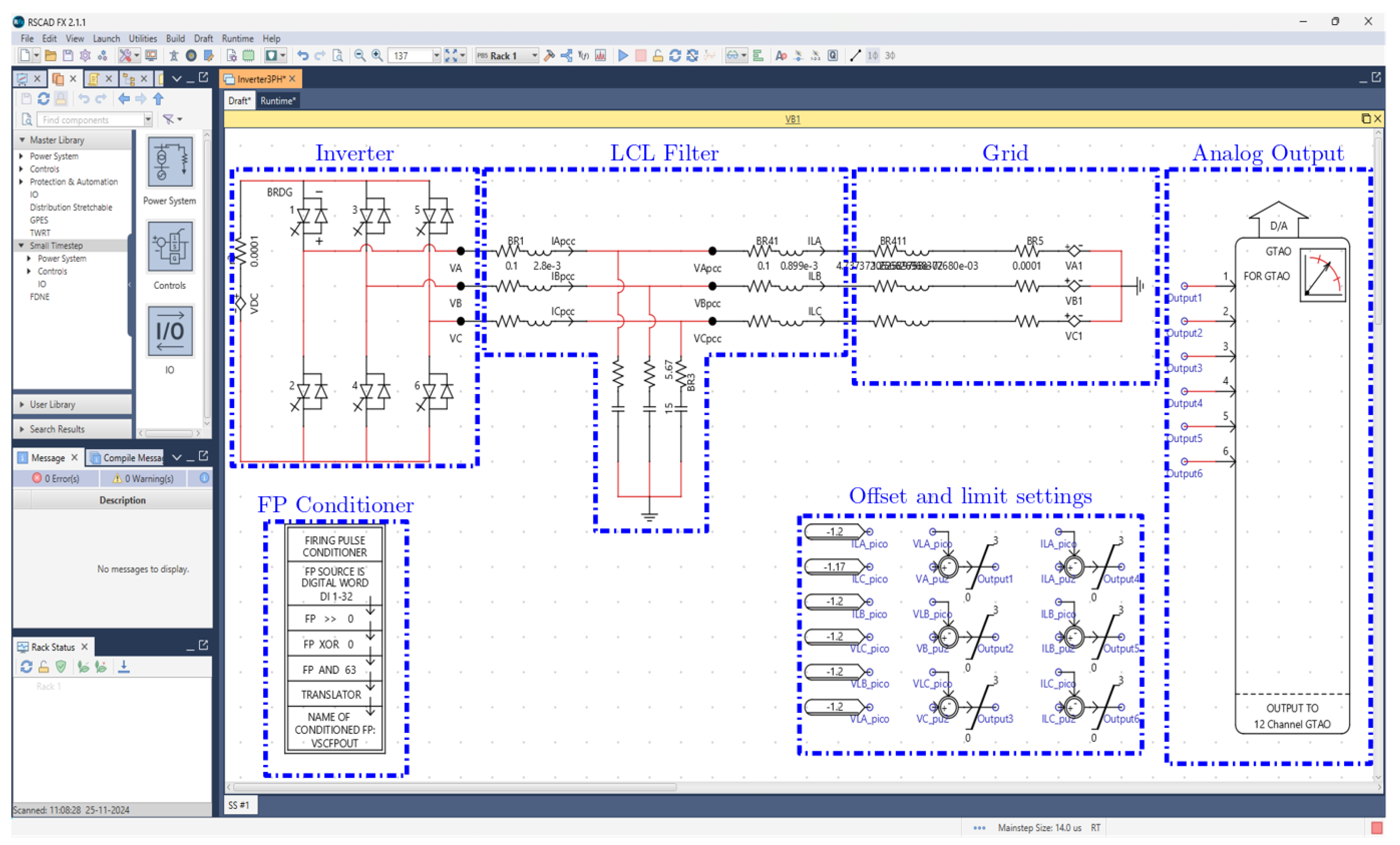
When running the CHIL simulation, it is necessary to perform additional tests to verify that the control laws are properly tuned to the inverter parameters. This is performed by changing reference variables and adjusting the DSP-clock timing to ensure the control can drive the three-phase inverter to different operating points. Figure 6 shows key parts of the simulation. The inverter must be configured to receive switching signals from each switch via the GTDI, ideally conditioned with a trigger pulse filter. The LCL filter must be accurately calculated, as CHIL would be ineffective without accounting for factors like power flow limits, direction, and resonant frequency. Lastly, the grid is selected according to the power capacities.

4.3. Methodology

An effective way to recognize inconsistencies or errors in the CHIL simulation is through understanding the implementation methodology. By properly understanding each component of the simulation, it is easier to identify mismatches in the system. Key steps in achieving this include the following:
  • Obtaining current and voltage signals from the system: This step is crucial to ensure that the initial conditions are representative of the real system.
  • Normalization and proper signal transmission to the DSP: Correct normalization ensures that the signals are correctly interpreted by the digital processor.
  • Implementation of the control laws within the DSP: It is critical that the control laws are implemented accurately to maintain the desired system performance.
  • Construction of PWM signals using control laws: PWM signals are essential for effective hardware control.
  • Reception of PWM signals in the RTDS: Correct reception and processing in the RTDS allows for the validation of the performance of the simulated system.

4.4. Analog I/O Path and DSP Integration

The signals acquired from the RTDS comprise the source-side currents and the grid-side voltages in the three-phase schematic. These are transmitted to the GTAO card. Upon measurement with an oscilloscope, an offset was detected, prompting the decision to attenuate it within the simulation. To comply with the development board’s security protocols, the signals were also constrained to a 0– 3 V range. Once correctly configured, it is possible to adjust various parameters in the software’s analog output block, including scaling, oversampling, and delay [19]. As shown in Figure 7, this process uses the voltage and current signals from the inverter in Figure 6 during real-time simulation. These signals, normalized to per-unit system, allow scaling within the DSP, enabling more effective control of system variables. After computing the phase and modulation amplitude for PWM generation, the control outputs the pulses through the DSP digital channels to the GTDI card, regulating the inverter in simulation. Analog inputs in Figure 7 are configured to ensure that changes to control reference variables do not affect the DSP analog output.

4.5. Timing and Delay Compensation

Several key factors must be considered. Delays from the GTAO board output are critical, as they can impair PLL synchronization and control precision. Even with concurrent system initiation, GTAO delays hinder accurate phase synchronization without a PLL. This highlights the importance of accounting for delays in systems requiring precise synchronization. Proper DSP-based control implementation in real-time simulation depends on all these aspects. These considerations are essential to ensure fidelity and performance.

5. Results

5.1. Test Bench and Operating Conditions

This section presents the results of the CHIL implementation of the inverter with the LCL filter. The plant is modeled in RTDS and the control is executed on a DSP F28379D, closing the loop using CHIL. As a preliminary validation, Model-in-the-Loop (MIL) simulations of the plant and controller are performed entirely in RSCAD/RTDS, without hardware or physical I/O, in two variants: averaged model and switched model of the converter. Based on this, the CHIL simulation is run with the switched model in RTDS and the control in the DSP. Then, the impedance response of the grid side obtained in CHIL is compared with the small-signal analytical model and the MILs, considering different scenarios of short-circuit capacity (SCC) and short-circuit ratio (SCR). Finally, the sensitivity of the CHIL signals with respect to the time step used in the RTDS is analyzed. All cases use the same three-phase inverter parameters and control laws. The control hardware operates with a sampling period of 30 μ s, a phase margin of 60 , and an approximate bandwidth of 75 Hz, in accordance with previously established guidelines.
The LCL filter parameters are listed in Table 1. The system operates at 60 Hz with a switching frequency of 2340 Hz. The inverter delivers 100 kVA to a 690 V grid. PLL gains were set to K p p l l = 12.25 and K i p l l = 1950 , and filter resistances R c and R g were both 0.1 Ω . Table 1 also includes three grid scenarios with different short-circuit capacities to assess performance under varying grid strengths.

5.2. Preliminary MIL and CHIL Validation

Figure 8a,b illustrate the dynamics of the voltage and current signals in the d q scheme of the RTDS implementation of the average model; since it is an average model, no oscillations due to switching or other factors that may affect the system are observed. Note that V d = 1.0203 pu and V q = 7.5885 × 10 6 pu .
Figure 9a,b represent the voltage and current signals in the d q scheme of the implementation of the switched model in RTDS; in this case, oscillations related to the switching of the PWM implemented in the system can be observed. To evaluate the performance of the model acurately, the root mean square error (RMSE) is computed for a steady state condition. The switched model achieves an RMSE of 0.0078 for the d axis and 0.0088 for the q axis. Similarly, for the currents, the RMSE reaches 0.0006 for both the d and q axes.
In the previous cases, the control laws were implemented within the same simulator. In Figure 10a,b, the dynamics of the voltage and current signals in the d q scheme were derived from the real-time simulation of the switched model, which incorporates the controller within the DSP and transmits PWM signals to the RTDS through the GTDI. For this scenario, the RMSE is calculated, yielding 0.0133 and 0.0095 for the d- and q-axis voltages, and 0.0089 and 0.0074 for the d- and q-axis currents. The analysis reveals that modeling under the CHIL concept is accurate, with a maximum error of 1.33% in the worst case.

5.3. Frequency Response Comparison

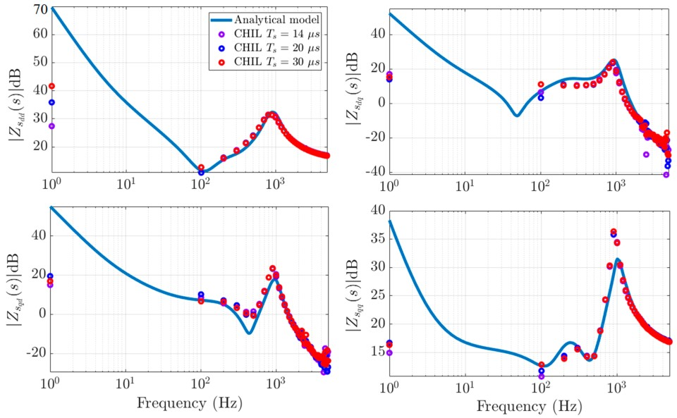
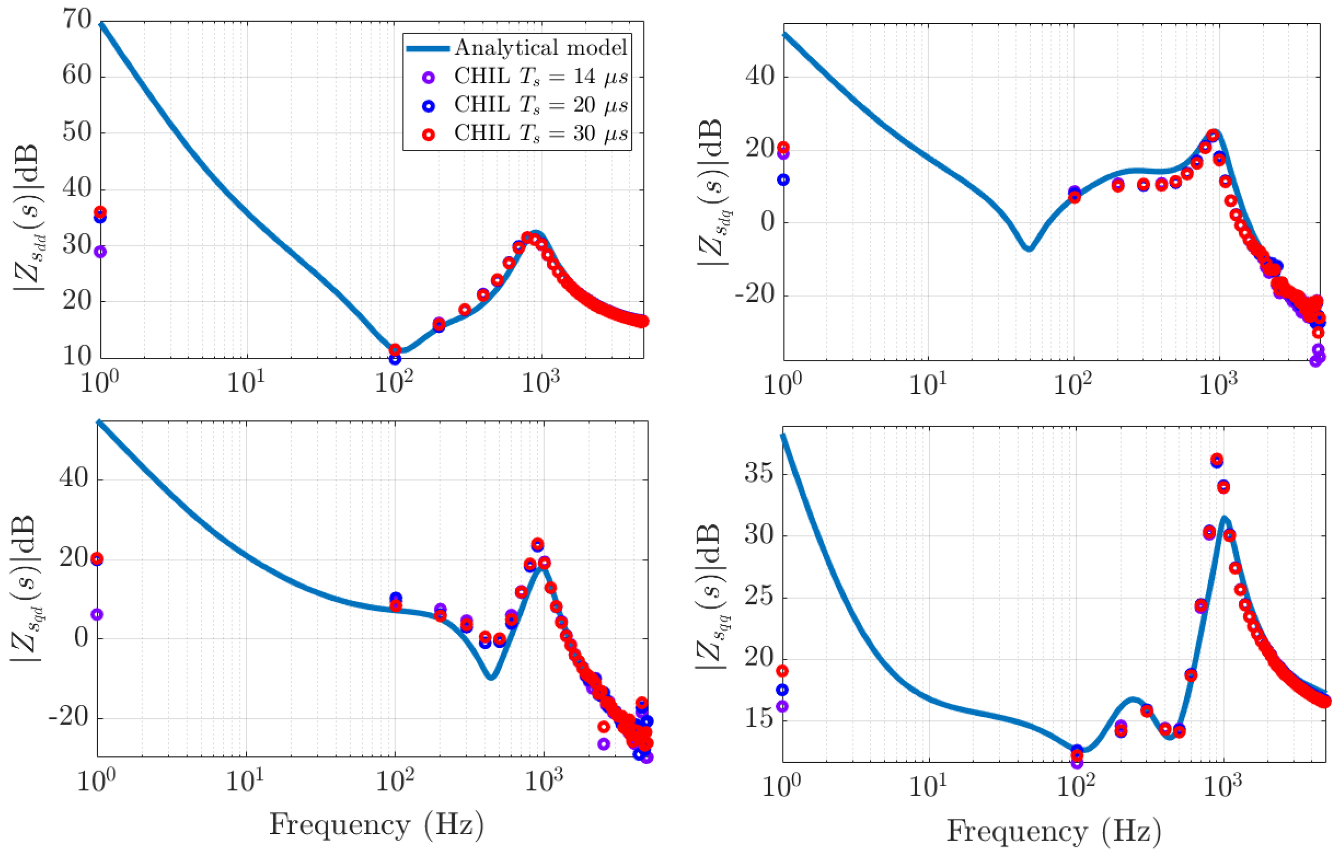
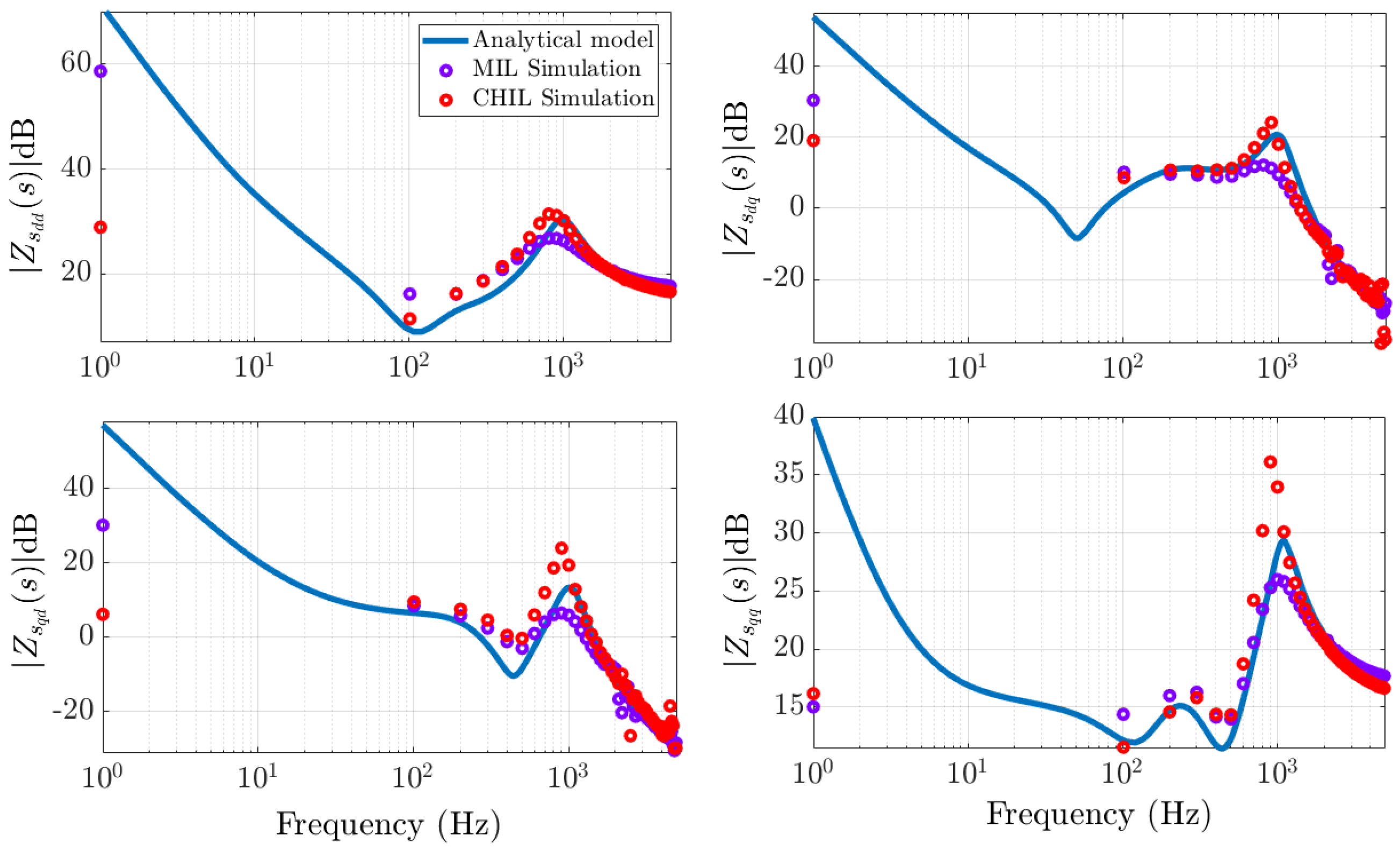
Impedance response is crucial for characterizing the operation and control of grid-connected converters [20,21]. A comprehensive evaluation of the CHIL setup with RTDS and a DSP card is conducted by comparing the impedance obtained via the perturbation method against that computed by the RTDS impedance computation module. This comparison employs the analytical model given by Equation (5) as a baseline. Three environments are assessed: (i) the analytical model, integrating the full set of differential equations; (ii) an MIL case, with plant and control running in RTDS; and (iii) a CHIL case, with the plant in RTDS and the controller on a DSP. In CHIL, three RTDS time steps ( 14 μ s , 20 μ s , and 30 μ s ) are analyzed to quantify step-size effects and contextualize performance relative to the analytical model and MIL. All cases use a switching frequency of 2340 Hz , with sampling times chosen to avoid missing PWM pulses. The model controlled by the development board (red circles) is compared with the analytical method (blue) and the RTDS implementation (purple circles). This comparison highlights differences in impedance response between the CHIL implementation and the other methods. Results show that, although all methods yield similar responses under ideal conditions, differences emerge under varying conditions. These indicate that CHIL may offer advantages in terms of stability and efficiency.As shown in Figure 11, the CHIL response is more accurate than that obtained with the control laws implemented in the RTDS.
As illustrated in Table 2, CHIL and MIL yield analogous RMSEs. CHIL demonstrates the lowest error in the d d channel, while in d q , q d , and q q , its RMSE is slightly higher than that of MIL. The RMSE was calculated in relation to the analytical model using only samples with frequencies greater than 100 Hz to mitigate low-frequency bias.
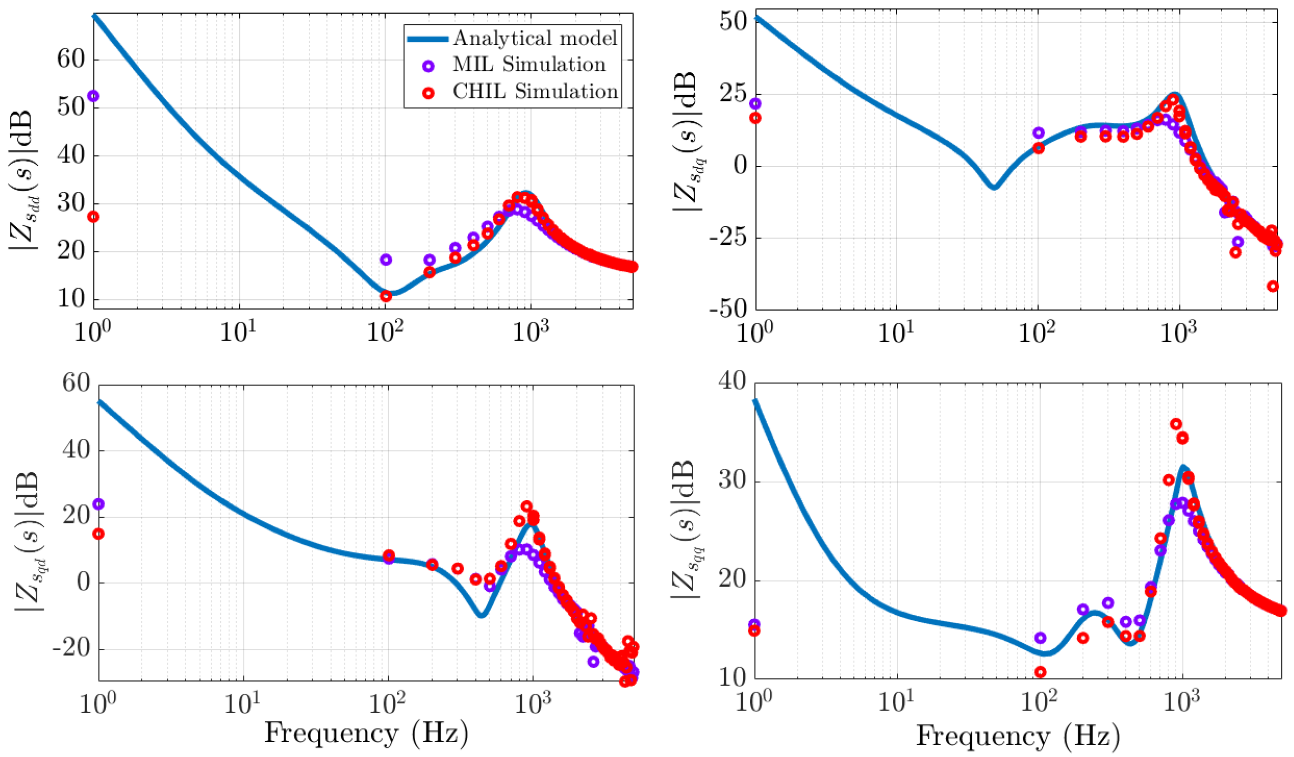
Further analysis is recommended to explore the practical implications of these results. Having compared frequency responses across different simulation types—and confirmed that the CHIL approach performs best, as seen in Figure 12, 14, and 16—an additional test was performed by increasing the RTDS simulation time step while keeping the DSP clock fixed at 30 μ s . In Figure 12, the same system is compared, but changes T s in the simulation within RTDS. As the time step increases, the response of the system remains the same, suggesting that, within this range of sampling times, the system is robust and is not significantly affected by changes in T s .
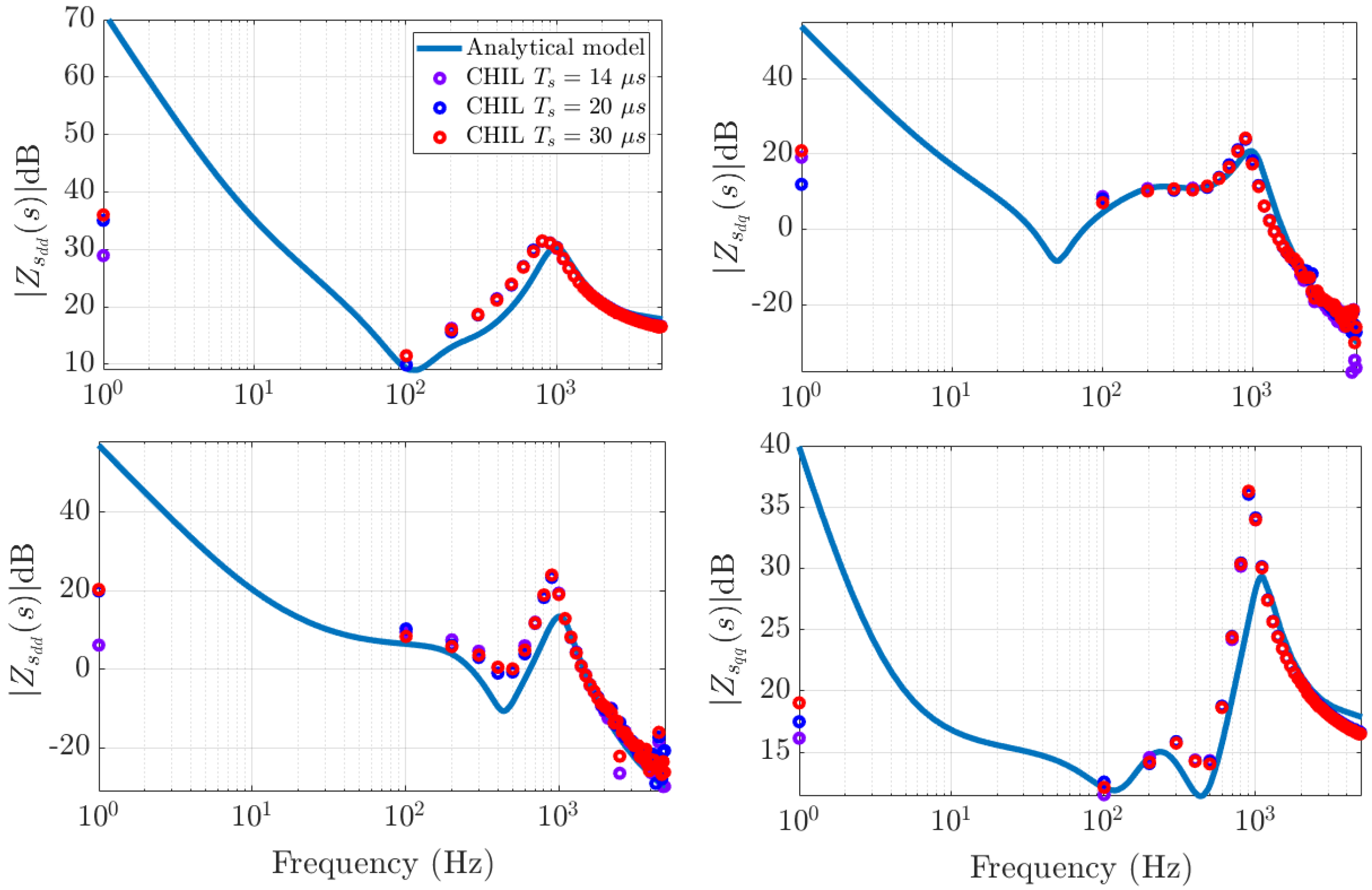
Figure 13 presents a comparison of the frequency responses derived from simulations executed with a system possessing a short-circuit capacity of 2.5 MVA. The data acquired from the CHIL simulation indicate that the system’s response remains satisfactory despite variations in short-circuit capacity.
Table 3 summarizes the RMSE between the analytical model and the MIL/CHIL simulations for a network with an SCC of 2.5 MVA. Overall, MIL and CHIL are comparable: CHIL achieves the lowest error in the d d channel, whereas its RMSE is slightly higher than that of MIL in d q , q d , and q q .
In Figure 14, it can be seen that the system maintains the same dynamics despite the large changes in T s and short-circuit capacity. This consistency suggests that the system is robust and capable of adapting to various operating conditions without compromising its performance.
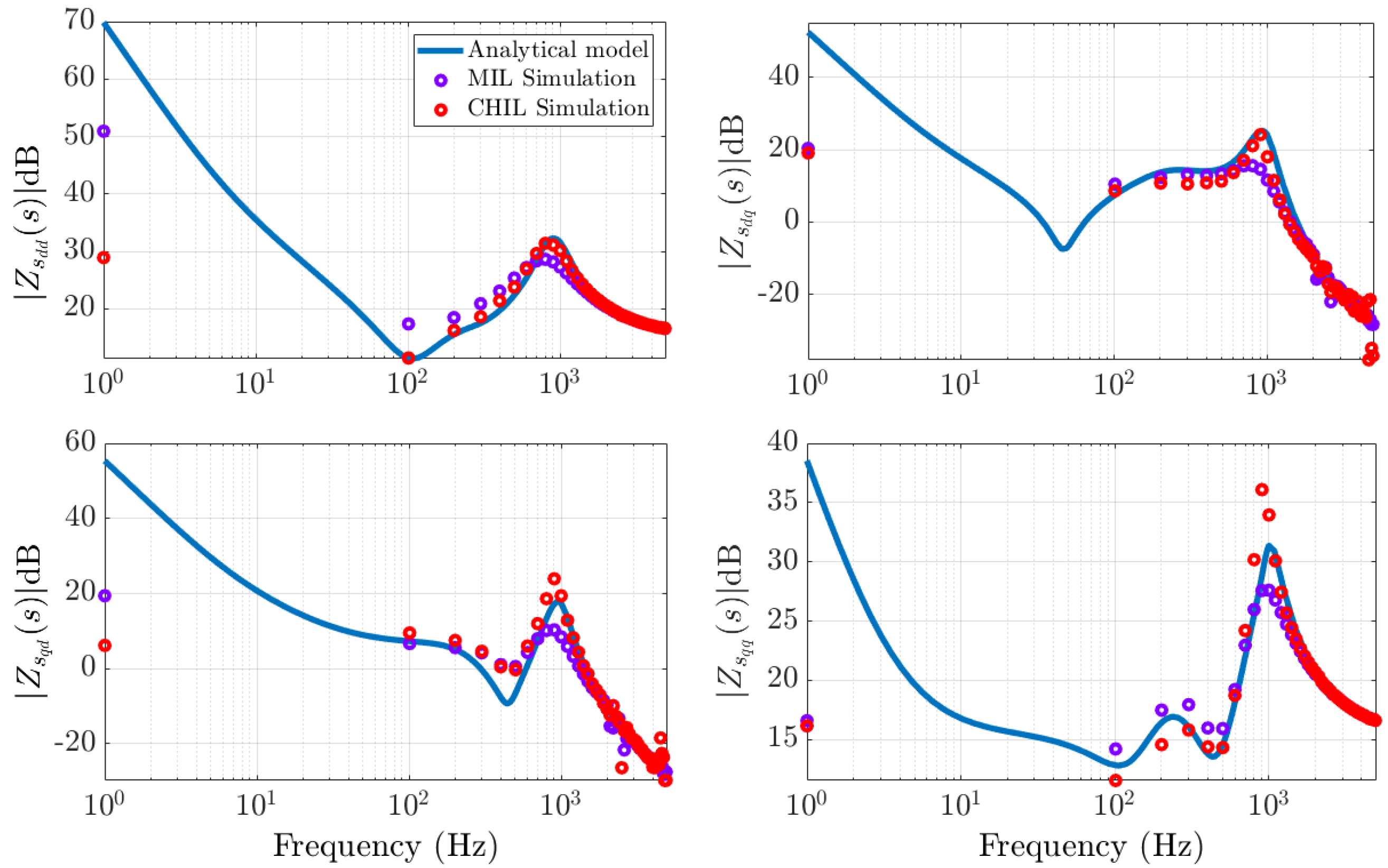
Finally, a comparison of the system with an SCC of 1 MVA is carried out. In Figure 15 and Figure 16, values very similar to those obtained earlier are obtained. Considering this, compared to the average model, the values obtained are stable and do not show abrupt changes when varying T s .
Table 4 summarizes the RMSE between the analytical model and the MIL and CHIL simulations for a network with SCC = 1.0 MVA. In general, the performance is comparable. In the d q element, CHIL has a smaller error than MIL. In d d , CHIL is slightly inferior to MIL, while in q d and q q , it is considerably superior. These figures quantify the difference in performance per element in the d-q framework.
Modifying the simulation time step alters the delay in the CHIL setup. Each compilation introduces a fixed delay of 9.203 μ s for signal transmission (GTAO to DSP) and 1.433 μ s for DSP processing and feedback (GTDI). These delays slightly affect the system response, as illustrated in Figure 12, Figure 14, and Figure 16.

6. Conclusions

Real-time simulators such as Typhoon, RTDS, Opal-RT, and dSPACE are widely used in power system analysis and testing due to their ability to simulate dynamic systems in real time. These simulators differ significantly in terms of accuracy and communication delays, which makes them suitable for various types of analyses. The main objective of this paper was to implement CHIL using a digital signal processor in a real-time simulation of a three-phase inverter interconnected to the grid. After the validation of the system response under the implemented control, a software tool was used to obtain the frequency responses. In general terms, the simulations performed were satisfactory, since the voltage and current signals showed a behavior in accordance with the theoretical expectations. Likewise, the frequency responses obtained from the average model and the real-time switched model showed consistent results, close to the values predicted by the analytical model. Comparison of results of the implementation of the control by means of the DSP allows us to demonstrate that the implementation of CHIL presents some differences in the impedance response in comparison with the other methods. However, the response of the CHIL implementation is the most accurate of the three approaches, since the DSP and its control are not just a model, but constitute a real device with its control implemented. This even considers the accuracy and speed limitations of the DSP, as well as the error introduced by control discretization and communication challenges. Our findings demonstrate that the CHIL approach with control implemented on a DSP accurately reproduces real dynamics by incorporating practical limitations on computational precision and speed, control discretization, and communication latencies. The comparison using RMSE against the analytical model shows that, although CHIL has lower error than MIL in several bands and channels, in other scenarios, the error increases. These discrepancies are attributed to quantization effects, unwanted sampling noise, and I/O delays. Despite this, when taking MIL as a reference and considering the positive correlation between the frequency responses of the averaged and switched models with the analytical formulation, the overall performance is deemed satisfactory.

Author Contributions

Conceptualization, J.S.-R. and L.C.H.M.; methodology, J.S.-R., J.C.H.R., Y.L.R. and L.C.H.M.; software, L.C.H.M., J.C.H.R. and Y.L.R.; validation, J.S.-R., L.C.H.M. and J.C.H.R.; formal analysis, J.S.-R., L.C.H.M. and J.C.H.R.; investigation, J.S.-R., L.C.H.M. and J.C.H.R.; resources, J.S.-R., N.V.-C. and E.B.; writing—original draft preparation, J.S.-R. and L.C.H.M.; writing—review and editing, J.S.-R., Y.L.R., N.V.-C. and E.B.; visualization, J.S.-R., E.B. and N.V.-C.; supervision, J.S.-R. and N.V.-C.; project administration, J.S.-R. and E.B.; funding acquisition, J.S.-R., N.V.-C. and E.B. All authors have read and agreed to the published version of the manuscript.

Funding

This research was funded by SECIHTI through the projects CF-2019/1311344, Faculty of Engineering at the Universidad Autonoma de San Luis Potosí.

Institutional Review Board Statement

Not applicable.

Informed Consent Statement

Not applicable.

Data Availability Statement

The code scripts and data can be obtained from the corresponding author upon request.

Acknowledgments

The authors want to acknowledge the Universidad Autónoma de San Luis Potosí through the Facultad de Ingeniería for the facilities granted to carry out this investigation. Leonardo Casey Hidalgo Monsiváis acknowledges the financial support received from SECIHTI through scholarship No. 836767 for his MSc studies, and scholarship No. 4042197 for his PhD studies. During the preparation of this work, the authors used Writefull and ChatGPT in order to improve language and readability, but not for text generation. After using these tools, the authors reviewed and edited the content as needed and take full responsibility for the content of the publication.

Conflicts of Interest

The authors declare no conflicts of interest.

Appendix A

Appendix A.1

The mathematical equations used to represent the dynamics of the closed-loop inverter are provided. Equations (A1) and (A2) define the currents on the source side, whereas Equations (A3) and (A4) pertain to the grid side.
d i C d t d t = ω 0 i C q t R c L c i C d t + V d c 2 L c v d m t 1 L c v C d t + R d L c i C q t i G d t
d i C q t d t = ω 0 i C d t R c L c i C q t + V d c 2 L q v q m t 1 L c v C q t + R d L c i C q t i G q t
d i G d t d t = ω 0 i G q t R g L g i G d t + 1 L g v C d t + 1 L g v G d t R d L g i C d t i G d t
d i G q t d t = ω 0 i G d t R g L g i G q t + 1 L g v C q t + 1 L g v G q t R d L g i C q t i G q t

Appendix A.2

The equations to express the behavior of the control laws shown in Figure 4 are the following [11]:
S d t = 2 V d c ω L c i C q t + u d t + e d t
S q t = 2 V d c ω L c i C d t + u q t + e q t
u d t = k p i d * t i C d t + x d t
u q t = k p i q * t i C q t + x q t
d x d t d t = k i i d * t i C d t
d x q t d t = k i i q * t i C q t

References

  1. Salas, A.B. Control Interactions in Power Systems with Multiple VSC HVDC Converters. Ph.D. Thesis, Faculty of Engineering Science, Leuven, Belgium, 2018. [Google Scholar][Green Version]
  2. Bashir, J.; Jena, P. Enhanced islanding detection scheme in distributed generation using phase angle analysis of negative sequence superimposed components. IEEE Trans. Ind. Electron. 2025, 1–10. [Google Scholar] [CrossRef]
  3. Avdiaj, E.; Lee, D.; Sakinci, Ö.C.; Beerten, J. Passivity-based design methodology for current-controlled grid-forming MMCs. IEEE J. Emerg. Sel. Top. Ind. Electron. 2025, 1–12. [Google Scholar] [CrossRef]
  4. Gupta, S.; Basumatary, K.; Shukla, A.; Gonzalez-Longatt, F. Real-Time Co-Simulation Platform for Grid-Forming BSS Using RTDS and FPGA. In Proceedings of the 2024 IEEE International Conference on Power System Technology (PowerCon), Kathmandu, Nepal, 4–6 November 2024; pp. 1–5. [Google Scholar]
  5. Basu, R.; Kuldip, C.; Kumar, M.; Lakshminarasamma, N. A Comprehensive Multi-stage Validation Approach for Development of Power Electronic Systems. In Proceedings of the 2024 IEEE 11th International Conference on E-Learning in Industrial Electronics (ICELIE), Chicago, IL, USA, 3–6 November 2024; pp. 1–5. [Google Scholar]
  6. Cha, S.T.; Wu, Q.; Nielsen, A.H.; ∅stergaard, J.; Park, I.K. Real-time hardware-in-the-loop (HIL) testing for power electronics controllers. In Proceedings of the 2012 Asia-Pacific Power and Energy Engineering Conference, Shanghai, China, 27–29 March 2012; pp. 1–6. [Google Scholar]
  7. Hidalgo Monsiváis, L.C. Three-Phase Inverter Control in Power Systems: Modeling, Simulation, and Hardware-in-the-Loop Validation. Master’s Thesis, Universidad Autónoma de San Luis Potosí, San Luis Potosí, Mexico, 2024. Available online: https://ciep.ing.uaslp.mx/alumnosPos/getTesis.php?f=20994246972202.pdf&c=246972 (accessed on 9 July 2025).
  8. Soomro, J.B.; Chachar, F.A.; Munir, H.M.; Ahmed Ansari, J.; Zalhaf, A.S.; Alqarni, M.; Alamri, B. Efficient hardware-in-the-loop and digital control techniques for power electronics teaching. Sustainability 2022, 14, 3504. [Google Scholar] [CrossRef]
  9. Kim, Y.J.; Wang, J. Power hardware-in-the-loop simulation study on frequency regulation through direct load control of thermal and electrical energy storage resources. IEEE Trans. Smart Grid 2016, 9, 2786–2796. [Google Scholar] [CrossRef]
  10. Faruque, M.O.; Strasser, T.; Lauss, G.; Jalili-Marandi, V.; Forsyth, P.; Dufour, C.; Dinavahi, V.; Monti, A.; Kotsampopoulos, P.; Martinez, J.A.; et al. Real-time simulation technologies for power systems design, testing, and analysis. IEEE Power Energy Technol. Syst. J. 2015, 2, 63–73. [Google Scholar] [CrossRef]
  11. Yazdani, A.; Iravani, R. Voltage-Sourced Converters in Power Systems: Modeling, Control, and Applications; John Wiley & Sons: Hoboken, NJ, USA, 2010. [Google Scholar]
  12. Franklin, G.F.; Powell, J.D.; Emami-Naeini, A. Feedback Control of Dynamic Systems, 8th ed.; Pearson Education Limited: Harlow, UK, 2019. [Google Scholar]
  13. Ramírez, J.C.H. Estabilidad Armónica en Microrredes de Corriente Alterna Interconectadas a la Red. Master’s Thesis, Universidad Autónoma de San Luis Potosí, San Luis Potosí, Mexico, 2017. [Google Scholar]
  14. Hernández-Ramírez, J.; Segundo-Ramírez, J.; Visairo, N.; Nuñez, C. Application of the Impedance-Based Method in Power Electronics: A Step-by-Step Review. In Proceedings of the 2021 IEEE International Autumn Meeting on Power, Electronics and Computing (ROPEC), Ixtapa, Mexico, 10–12 November 2021; Volume 5, pp. 1–6. [Google Scholar]
  15. Kazmierkowski, M.P.; Malesani, L. Current control techniques for three-phase voltage-source PWM converters: A survey. IEEE Trans. Ind. Electron. 1998, 45, 691–703. [Google Scholar] [CrossRef]
  16. RTDS Technologies Inc. RTDS—Real-Time Digital Simulator; RTDS Technologies Inc.: Winnipeg, MB, Canada, 2021; Available online: https://www.rtds.com (accessed on 1 October 2024).
  17. Åström, K.J.; Wittenmark, B. Computer-Controlled Systems: Theory and Design; Courier Corporation: Chelmsford, MA, USA, 2013. [Google Scholar]
  18. Popovici, K.; Mosterman, P.J. Real-Time Simulation Technologies: Principles, Methodologies, and Applications; CRC Press: Boca Raton, FL, USA, 2017. [Google Scholar]
  19. Texas Instruments. TMS320F2837xD Dual-Core Real-Time Microcontrollers; Texas Instruments: Dallas, TX, USA, 2024; Available online: https://www.ti.com/lit/ds/symlink/tms320f28379d.pdf (accessed on 3 November 2024).
  20. Gu, H.; Guo, X.; Wang, D.; Wu, W. Real-time grid impedance estimation technique for grid-connected power converters. In Proceedings of the 2012 IEEE International Symposium on Industrial Electronics, Hangzhou, China, 28–31 May 2012; pp. 1621–1626. [Google Scholar]
  21. Sun, J. Impedance-based stability criterion for grid-connected inverters. IEEE Trans. Power Electron. 2011, 26, 3075–3078. [Google Scholar] [CrossRef]
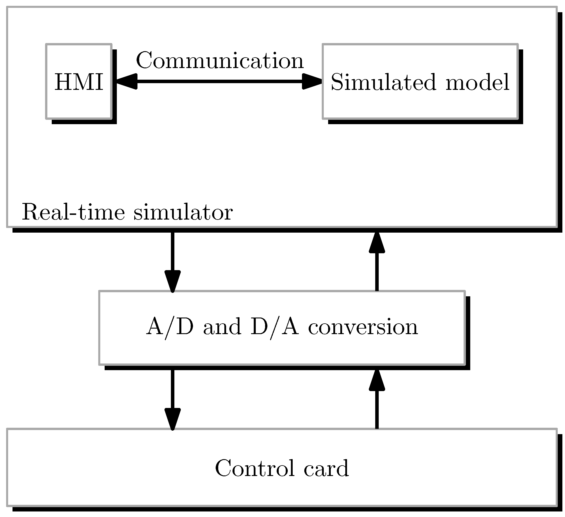
Figure 1. Basic CHIL simulation concept, including the human–machine interface (HMI), and digital-to-analog (D/A) and analog-to-digital (A/D) converters [10].
Electricity 06 00052 g001
Figure 2. Three-phase grid-connected inverter.
Electricity 06 00052 g002
Figure 3. PLL block diagram.
Electricity 06 00052 g003
Figure 4. Block diagram of the implemented control.
Electricity 06 00052 g004
Figure 5. Scheme implemented in laboratory.
Electricity 06 00052 g005
Figure 6. Implementation within the software.
Electricity 06 00052 g006
Figure 7. Implementation of the TMS320F28379D board.
Electricity 06 00052 g007
Figure 8. Voltages and currents in the dq reference frame of the average model in RTDS. (a) Voltages. (b) Currents.
Electricity 06 00052 g008
Figure 9. Voltages and currents on the source side in the d q scheme of the RTDS switched model (a) Voltages. (b) Currents.
Electricity 06 00052 g009
Figure 10. Voltages and currents at the PCC in the d q scheme of the switched model in RTDS and control hardware in DSP. (a) Voltages. (b) Currents.
Electricity 06 00052 g010
Figure 11. Source-side impedance transfer functions (5 MVA SCC).
Electricity 06 00052 g011
Figure 12. Time step impact on source-side impedance responses: CHIL study (5 MVA SCC).
Electricity 06 00052 g012
Figure 13. Source-side impedance transfer functions (2.5 MVA SCC).
Electricity 06 00052 g013
Figure 14. Time step impact on source-side impedance responses: CHIL study (2.5 MVA SCC).
Electricity 06 00052 g014
Figure 15. Source-side impedance transfer functions (1 MVA SCC).
Electricity 06 00052 g015
Figure 16. Time step impact on source-side impedance responses: CHIL study (1 MVA SCC).
Electricity 06 00052 g016
Table 1. System parameters.
ParameterScenario 1Scenario 2Scenario 3
SCC5 MVA2.5 MVA1 MVA
L c 3.54 mH 3.52 mH 2.8 mH
L g 2.37 mH 7.93 mH 2.15 mH
R d 5.09 Ω 4.88 Ω 5.67 Ω
C13.5 μ F13.88 μ F15 μ F
K p d q 2.992.862.51
K i d q 105.22110.11125.08
S C R 502510
Table 2. RMSE per d-q element of Z s , comparing analytical model with MIL and CHIL simulations (SCC = 5 MVA, f 100 Hz).
ChannelRMSE MIL SimulationRMSE CHIL Simulation
d d 1.81470.67422
d q 4.06764.1725
q d 1.13611.4164
q q 3.2643.7677
Table 3. RMSE per d-q element of Z s , comparing the analytical model with MIL and CHIL simulations (SCC = 2.5 MVA, f 100 Hz).
ChannelRMSE MIL SimulationRMSE CHIL Simulation
d d 1.76440.66472
d q 3.85373.776
q d 3.15283.3321
q q 1.1621.4195
Table 4. RMSE per d-q element of Z s comparing analytical model with MIL and CHIL simulations (SCC = 1 MVA, f 100 Hz).
ChannelRMSE MIL SimulationRMSE CHIL Simulation
d d 1.84321.7482
d q 4.12073.7659
q d 1.2052.4042
q q 3.27564.764
Disclaimer/Publisher’s Note: The statements, opinions and data contained in all publications are solely those of the individual author(s) and contributor(s) and not of MDPI and/or the editor(s). MDPI and/or the editor(s) disclaim responsibility for any injury to people or property resulting from any ideas, methods, instructions or products referred to in the content.