Article

Low-Cost Active Power Filter Using Four-Switch Three-Phase Inverter Scheme

Electrical Engineering Department, Yanbu Industrial College, Yanbu 46452, Saudi Arabia
Electricity 2025, 6(1), 16; https://doi.org/10.3390/electricity6010016
Submission received: 4 February 2025 / Revised: 7 March 2025 / Accepted: 11 March 2025 / Published: 17 March 2025

Abstract

:
Shunt active power filters (SAPFs) have been around for a long time. They improve the quality of a current drawn from the grid when feeding non-linear loads formed by old-fashioned power electronic converters such as uncontrolled and controlled rectifiers. Most SAPFs are implemented using the well-known six-switch three-phase inverter (SSTPI) topology. This paper investigates the capability of adopting the four-switch three-phase inverter (FSTPI) scheme to develop low-cost SAPFs, mainly for low-power ranges. The performance of the proposed SAPF using the FSTPI topology is compared with the conventional scheme of an SAPF formed by the six-switch three-phase inverter (SSTPI) topology. Qualitative and quantitative analyses are conducted. The performance of the proposed FSTPI-based SAPF is investigated under different loading conditions. The obtained results indicate the validity and effectiveness of the FSTPI scheme in improving the quality of currents drawn from the AC grid. The SAPF scheme investigated is also feasible and results in cost reduction when the SAPF power circuit is constructed with modern WBG devices, such as SiC-based MOSFETs, which are relatively expensive (approximately three times the price of the equivalent Si IGBTs).

1. Introduction

The concept and idea of active power filters (APFs) based on current injection into the grid to offset undesired load harmonics were proposed several decades ago [1]. However, this topic is still of considerable interest for investigation [2,3,4,5,6,7,8,9,10,11,12,13]. The main idea of APFs is to inject a current into the electric grid (AC source) at the point of common coupling (PCC) to cancel out the undesired harmonics caused by non-linear loads which are fed from the AC source. The compensating currents injected by the APF must have the same amplitude and the opposite phase to the undesired harmonic components of the non-linear load. Consequently, the resultant grid currents are sinusoidal waveforms and in-phase with the grid voltages for unity PF operation [2,3]. Mainly, the control system of the APF should guarantee a good current tracking capability and low total harmonic distortion (THD) in the grid currents. In addition to this, it should provide good DC bus voltage regulation. Therefore, successful APFs accomplish harmonic standards, such as IEEE 519, improving the power quality requirements [2]. Several efforts have been carried out to study and investigate the performance of active power filters. In Ref. [1], detection and control techniques for harmonic currents were addressed. It also introduced modeling and stability analysis methods for the multi-parallel SAPF system. In Ref. [3], a shunt hybrid active power filter for 1 kV mining applications was implemented. The control technique involved time delay compensation and voltage distortion compensation. Refs. [4,5] presented various control techniques for APFs. In Ref. [4], a feedback-linearization-type approach to control the currents of an APF was presented. It included a DC-side voltage control loop beside the current control loop. The main feature of the proposed control method was the compensation of the time delay caused by microcontroller computation using a finite impulse response predictor.
In Ref. [5], a deadbeat-based direct power control method to generate a reference current and control of the active power filter was proposed. The THD of the steady-state grid current was reduced from 22% to 3%. In [6], an adaptive DC-link voltage control for shunt active power filters was proposed. The method was based on the model predictive current control approach. The proposed control method could regulate the DC-link voltage according to grid voltage fluctuations. In references [7,8,9], active power filters were controlled under unbalanced electric grid conditions. The control technique in [7] relies on the modular fundamental element detection method, which can manage the mitigation of harmonic currents under an unbalanced and/or distorted grid. In [8], a Kalman filter was employed to obtain the fundamental sequence component of the grid voltage. Meanwhile, in [9], the controller of the shunt active power filter required only current measurements without any voltage measurements. The THD of the grid currents was reduced to a satisfactory level. On the other hand, evolutionary search algorithms have been employed for the control of active power filters, as investigated in [10]. Recently, an artificial intelligence approach was employed for the control of active power filters. Ref. [11] proposed a machine learning-based controller for a shunt active power filter. It can be considered as a universal machine learning controller that can generate reference currents for an active power filter. Moreover, the sliding mode control technique was applied for the control of active power filters, as presented in [12]. On the other hand, the pioneer contributions and early works of the four-switch three-phase inverter (FSTPI) topology were addressed in references [13,14,15,16,17,18], where modulation techniques for the FSTPI scheme were proposed. The results demonstrated that the FSTPI topology would be competitive compared to the commonly used six-switch three-phase inverter (SSTPI) scheme in the low-power range. Recently, the FTPI topology was utilized to develop active power filters, as indicated in [19]. Authors in [19] adopted the fundamental positive sequence extraction method, which does not require a phase-locked loop or complex coordinate transformation. On the other hand, generation methods for reference currents for SAPFs have received great attention from researchers. Various methods have been developed to operate shunt active power filters [20,21,22,23,24]. All research activities aim to accomplish the existing IEEE standards of [25,26,27]. Thus, the current injected by APFs should result in an overall current drawn from the AC mains that satisfies the criteria of these IEEE standards.
The DC bus voltage is well-regulated using conventional or improved PI controllers, where the output of the voltage controller represents the reference signal of the grid current. References [28,29,30] addressed some efficient harmonic extraction algorithms and methods to generate reference grid current signals based on the extraction of the first harmonic of the load currents.
The rest of the paper is organized as follows: Section 2 summarizes the main objectives and contributions of the paper. Section 3 presents the principles and main concept of the shunt active power filter. Section 4 explains the generation methods for reference grid currents. Section 5 addresses the principle of operation of the FSTPI. Section 6 presents the investigated schemes of the SAPF, while Section 7 presents some simulation results of different operating conditions, including qualitative and quantitative assessments. Section 8 includes the conclusions and findings. Tables of abbreviations and symbols are provided as well. Finally, a list of references is provided.

2. Objective and Contribution of the Paper

2.1. Main Objective

This paper investigates the performance of a shunt active power filter (SAPF) using a four-switch three-phase inverter (FSTPI) topology to develop a high-performance SAPF with reduced cost. A comparison between the conventional six-switch three-phase inverter (SSTPI) scheme is carried out. Based on the results, the feasibility of such an SAPF scheme can be assessed.

2.2. Main Contribution

The FSTPI-based SAPF system is studied in different operating conditions, including a highly inductive nonlinear load, highly distorted load, and unbalanced nonlinear load. A comprehensive performance analysis of the investigated SAPF scheme, including qualitative and quantitative assessments, is made. In addition, the proposed SAPF scheme is compared with the conventional SSTPI-based SAPF topology to determine to which degree the proposed scheme is successful and feasible.

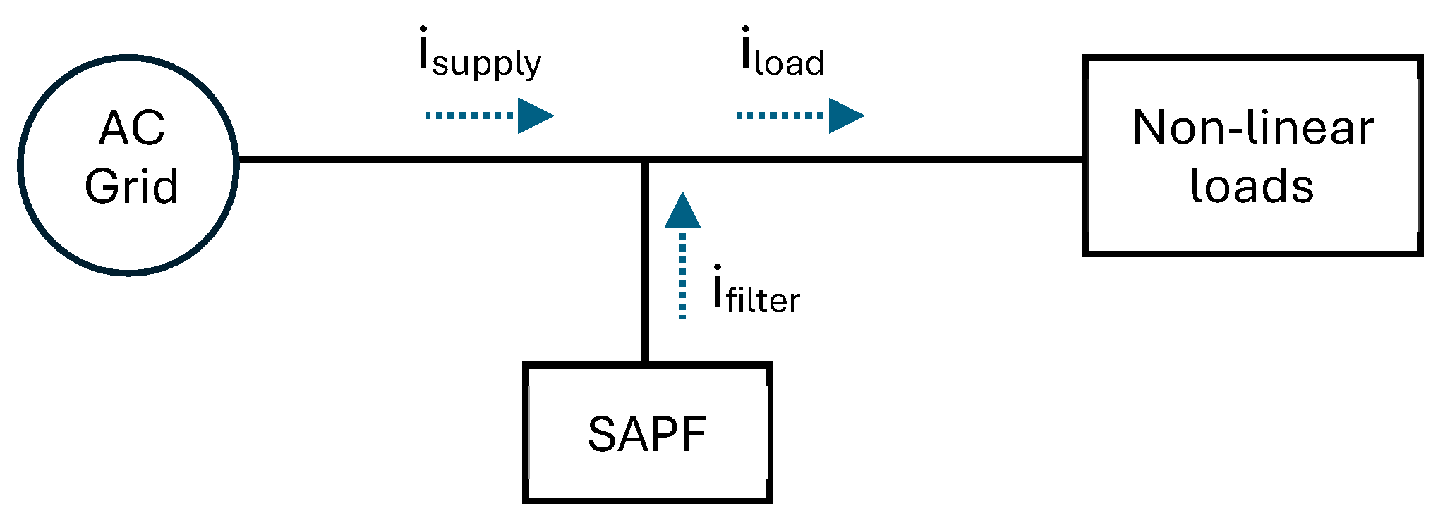
3. Concept of Shunt Active Power Filter

The three-phase SAPF injects currents into the electric grid that cancel out undesired harmonics caused by non-linear loads fed from the AC source [3]. The SAPF compensating currents have the same amplitude and are out of phase with the harmonic components caused by the non-linear load. Consequently, this results in a sinusoidal grid current by the power quality standards. A simplified block diagram of the shunt active power filter is illustrated in Figure 1, where the SAPF injects currents into the grid that compensate for or eliminate the effect of non-linear loads such that the net currents drawn from the AC supply are near sinusoidal waveforms with a minimum possible THD.
Thus, Equations (1) and (2) are valid, as follows:
i s u p p l y + i f i l t e r = i l o a d
i f i l t e r = i l o a d i s u p p l y
A circuit diagram of a typical SAPF system is shown in Figure 2, where the power circuit of the SAPF is based on the conventional SSTPI (B6) topology. The non-linear load would be equipment or an appliance that is fed from an uncontrolled rectifier. Also, it can be a DC drive, fed from a SCR phase-controlled converter. Such non-linear loads deteriorate the power quality of the AC grid in terms of the line current harmonic content, high THD of the line currents, and spikes superimposed on the grid voltage. The reference filter currents are computed using Equation (3), as follows:
i f a i f b i f c = i L a i L b i L c i s a i s b i s c
where i f a ,   i f b , and i f c are the reference filter currents; i L a , i L b , and i L c are the instantaneous values of the load currents; and i s a ,   i s b , and i s c are the reference grid currents. The actual SAPF filter currents can be controlled using hysteresis current controllers to track (follow up) their corresponding reference values. The hysteresis current controller can be a conventional ON–OFF controller with a tolerance band or a PI controller incorporated with a PWM to operate at a fixed switching frequency (to be discussed later in Section 6).
If the reference grid currents are sinusoidal signals with optimum amplitudes, the corresponding reference filter currents will be the difference between the load currents and the reference grid currents (sinusoidal signals). Hence, the instantaneous values of the filter currents that are injected into the grid result in sinusoidal grid currents with a satisfactory THD and well attenuated harmonic content that matches the existing standards [25,26].

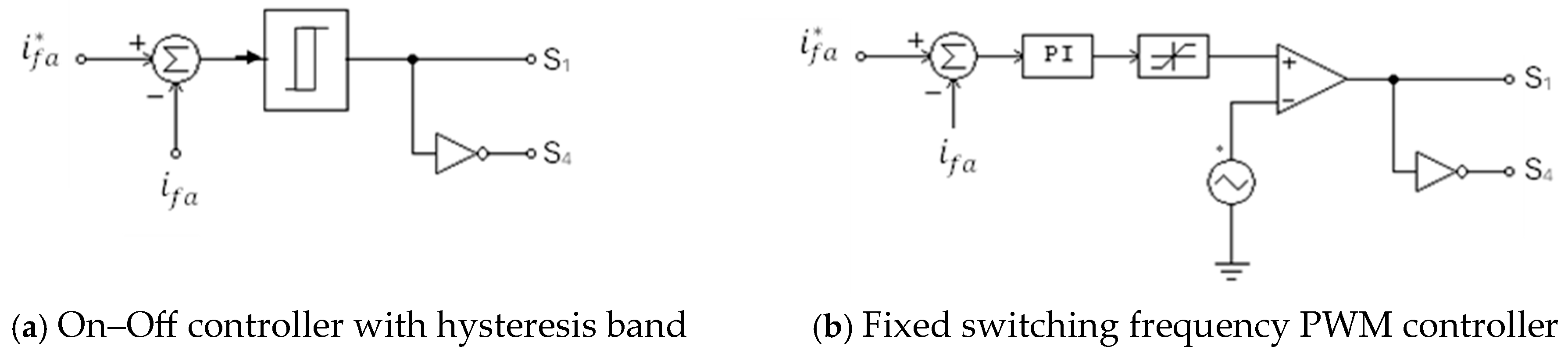
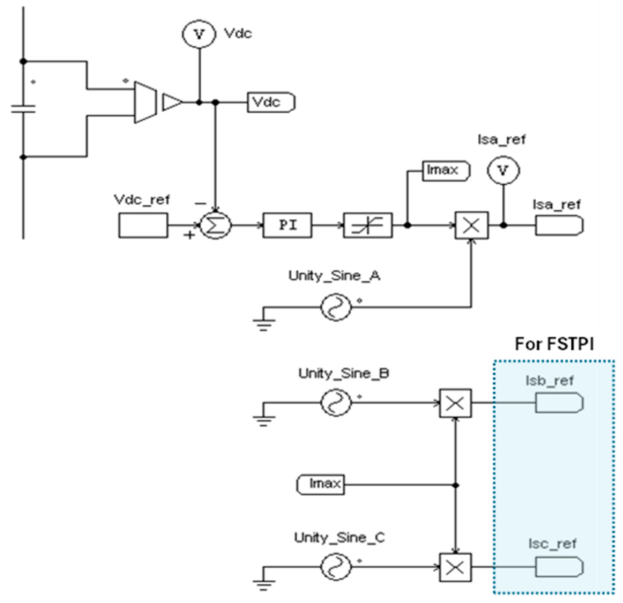
4. Reference Grid Currents Generation Methods

The control system of the SAPF consists of the following parts (units): (1) the generation of the reference grid (supply) current; (2) the generation of the reference compensating current of the SAPF; (3) current controllers of the voltage source PWM converter; and (4) the voltage controller of the DC bus voltage of the voltage source PWM converter (when the DC bus is a DC capacitor not a DC supply). The generation of reference compensating current plays an important role that affects the filtering performance, since any reference compensating currents with an inaccurate phase or magnitude can result in degradation in the compensation process. Various methods have been proposed to generate these reference signals. Harmonic current detection techniques and harmonic current control techniques were addressed in [1], where the advantages and disadvantages of various algorithms were presented.
One main approach is based on the closed-loop control of the DC link voltage of the SAPF, as explained in [20,21,22]. Others generate reference signals based on the extraction of the first harmonic of the load currents, as proposed in [28,29,30].

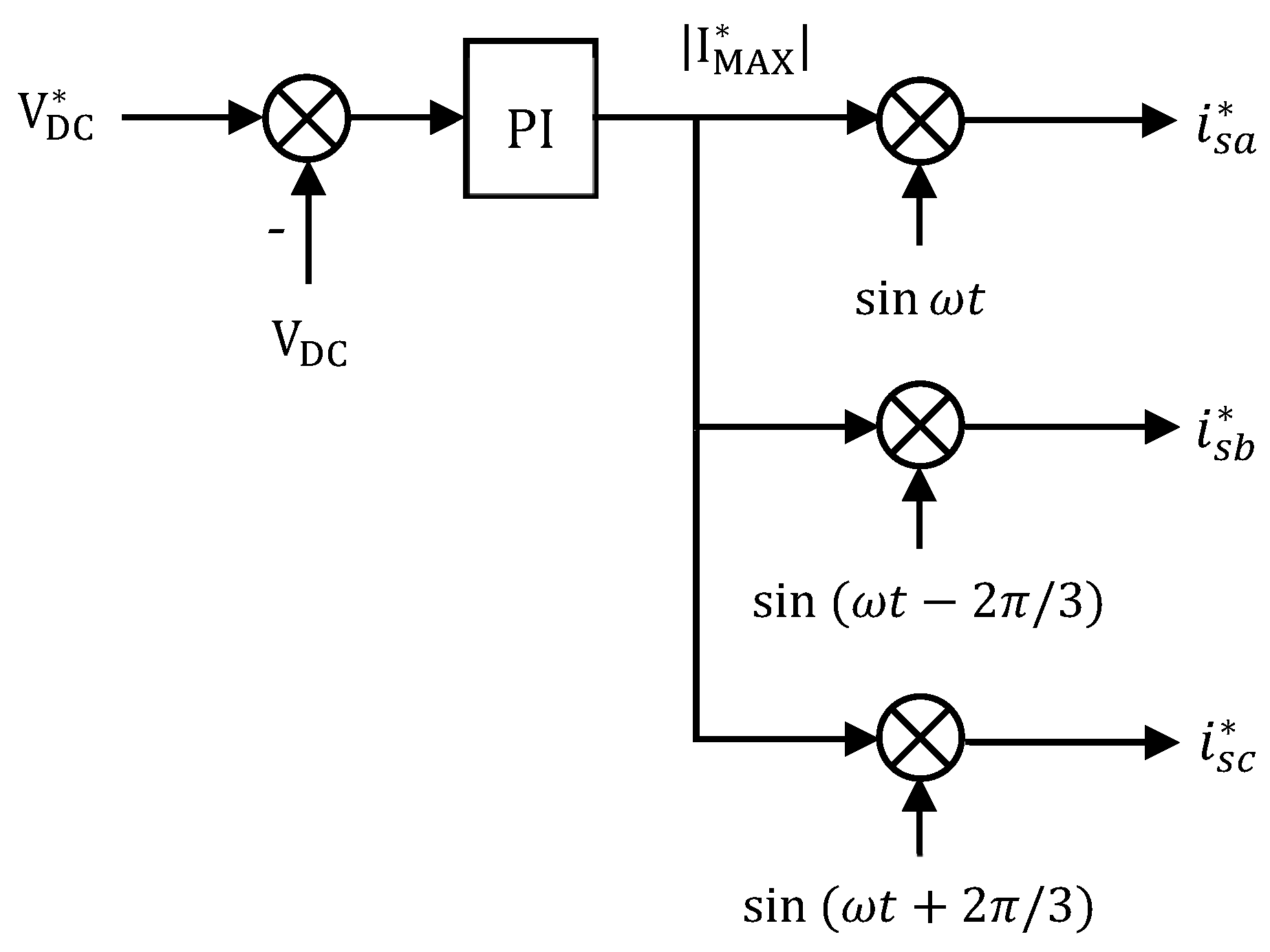
4.1. Based on Closed-Loop Control of DC Link Voltage of the SAPF

The DC link side of the SAPF “capacitor voltage” is regulated using a closed-loop controller. Well-known PI controllers with a limited output are usually employed. Recently, fractional-order PI controllers can be employed as well. The output of the voltage controller is considered the reference amplitude, with the “maximum value” of the current to be drawn from the supply. To generate the three-phase sinusoidal reference signals, three-phase unity sinusoidal waveforms are employed, as illustrated in Figure 3.
The method shown in Figure 3 is simple to implement. However, in the case of severe supply voltage distortion, PLLs can be utilized to generate the reference sinusoidal waveforms of the grid currents. Once the reference grid currents are calculated, they can be utilized to generate the reference filter current owing to Equation (3).

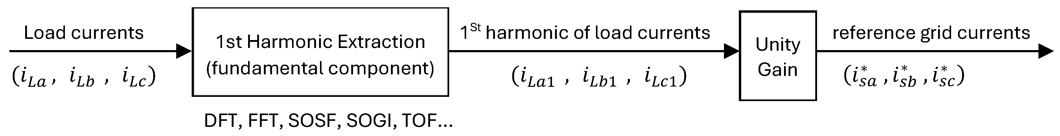
4.2. Based on Calculation of the First Harmonics of the Load Current

The reference grid current is computed based on the extraction of the fundamental component of the non-linear load current, where the reference grid currents ( i s a   ,   i s b   ,   i s c ) equal the calculated fundamental components of the load current ( i L a 1   ,   i L b 1   ,   i L c 1 ) , respectively, as shown in Figure 4. Several efficient harmonic extraction algorithms with good accuracy have been proposed, such as the methods of references [29,30].
Harmonic extraction techniques are carried out in the time domain or the frequency domain [31]. The well-known or commonly used frequency domain-based methods are Discrete Fourier Transform (DFT) or the Fast Fourier Transform (FFT), Second-Order Sequence Filter (SOSF), Second-Order Generalized Integrator (SOGI), and others. Time-domain-based methods such as Instantaneous Reactive Power Theory (IRPT) and Synchronous Reference Frame are also applied in SAPFs.
Recently, a method based on Trigonometric Orthogonal Function (TOF) was proposed [29].
Apart from the method employed for reference grid current generation, current controllers are used to control the operation of SAPFs. Figure 5 demonstrates two types of current controllers that are commonly used in the control of the operation of three-phase VSI inverters and active power filters.
The first type shown in Figure 5a is an ON–OFF controller with a predefined hysteresis (tolerance) band that can be set to any desired value. With this controller, the resultant switching frequency is not constant. If the hysteresis band is set to a value of zero or a small value, the resultant switching frequency will be very high, which increases the switching losses. Sometimes, it can burn the power transistors. The second type shown in Figure 5b provides an operation of PWM controller at a fixed switching frequency based on the frequency of the carrier signal (triangle waveform). Thus, this type provides a better performance.

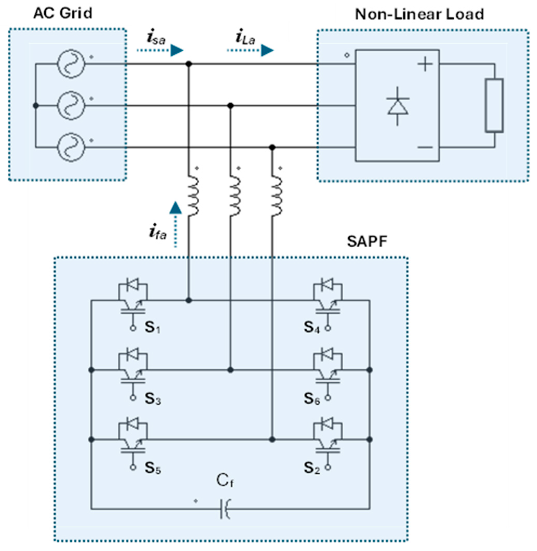
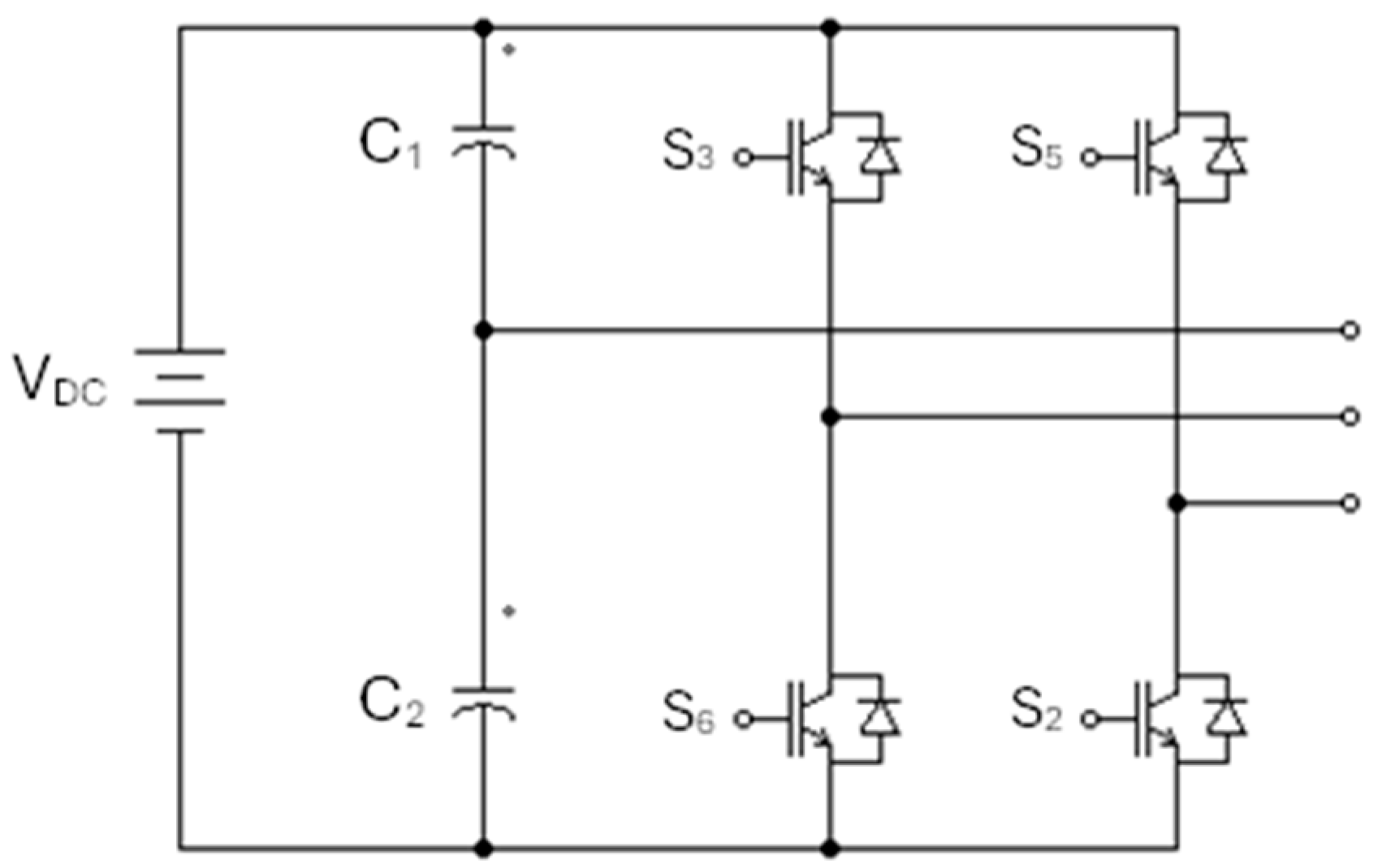
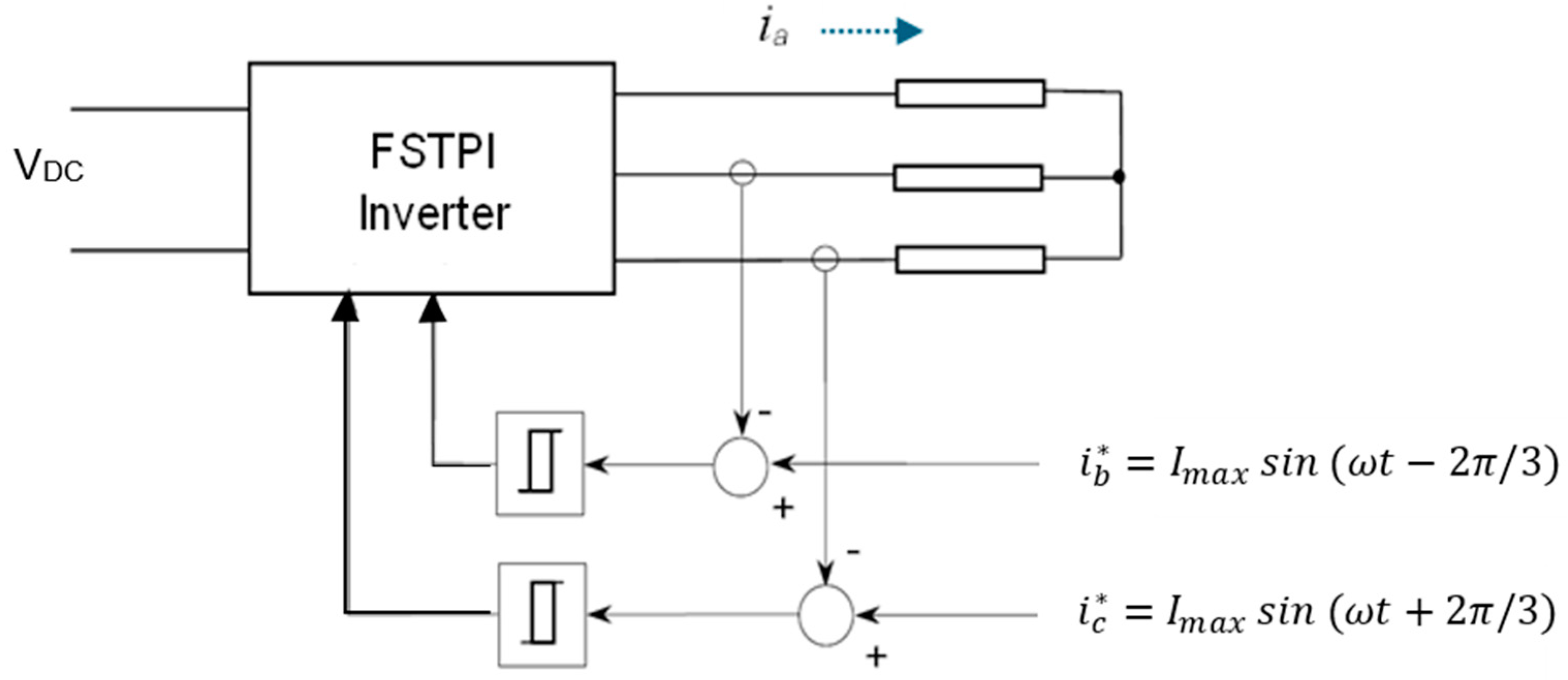
5. Principle of Operation of FSTPI

The FSTPI (B4) topology is composed of four power switches (transistor and antiparallel diode) forming two branches, while the third branch is formed by two identical capacitors. Figure 6 illustrates a circuit diagram of the FSTPI.
From the current point of view, for a balanced three-phase load, if the currents in the second and third phases (ib and ic) are controlled to be sinusoidal with a phase shift of 120° electrically from each other (See Figure 7), i.e., when i b and i c are sinusoidal, the current in the first phase (ia), which is connected to the capacitors, will be forced to be sinusoidal owing to the Equations (4) and (5) given as follows:
i a + i b + i c = 0
i a = ( i b + i c )
Thus, theoretically, the function and operation of the SAPF can be carried out successfully using the FSTPI topology. In this case, the currents i f b and i f c (injected from the SAPF) are controlled using hysteresis current controllers. Hence, the current in the first phase ( i f a ) is indirectly regulated to have the same waveform as the two other phases b and c.
Adopting the FSTPI scheme in SAPFs results in a reduction in the number of the required isolation/driver circuits and isolated power supplies from six to four circuits. Thus, a saving of 33% in the number of power switches and the corresponding auxiliary electronic circuits is achieved. Moreover, the system will require a reduced number of Hall effect current transducers, which reduces the overall cost of the SAPF as well. The extent of savings is clear when SiC power transistors are utilized to construct the SAPF power electronic circuit (converter power circuit) due to their relatively higher prices (almost three times the price of Si-based counterparts with the same rating). The voltage space vector of the four-switch 3-Φ inverter is computed using Equation (6), as follows:
V ¯ S = 2 3 V D C 0.5 + e j 2 π / 3 S 3 + e j 4 π / 3 S 5
When the previous equation is resolved in the (α–β) system of coordinates, the following components in the stationary reference frame are obtained by Equations (7) and (8):
v α = V D C 3 1 S 3 S 5
v β = v b c 3 = V D C 3 S 3 S 5
Since the inverter is composed of four switches, only four switching states are available. Applying the Park transformation to the inverter output voltage yields the following facts:
  • The inverter provides only four active vectors [17].
  • The vectors are not equal. They have different magnitudes.
  • The vectors are displaced by 90 degrees electrically from each other [18].
  • The inverter does not provide any zero/nil vectors [17,19].

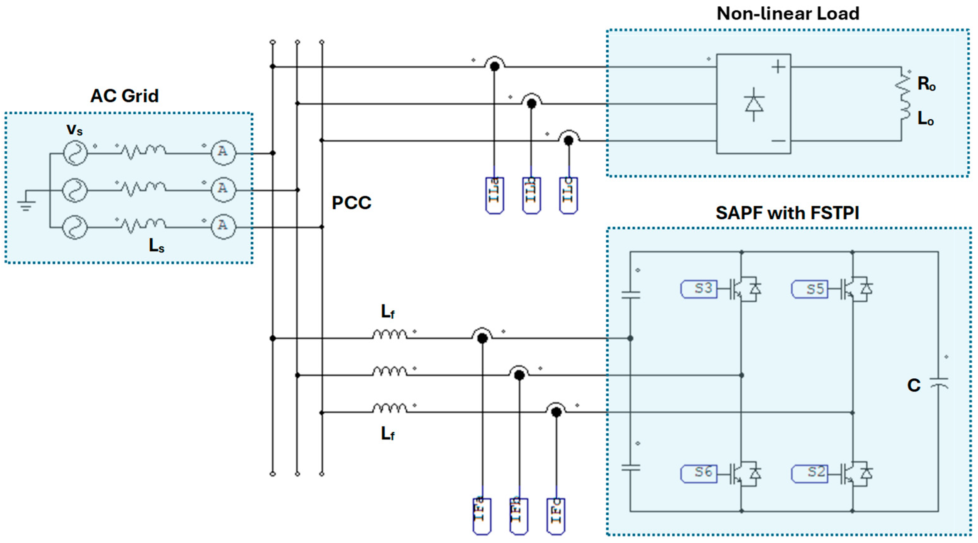
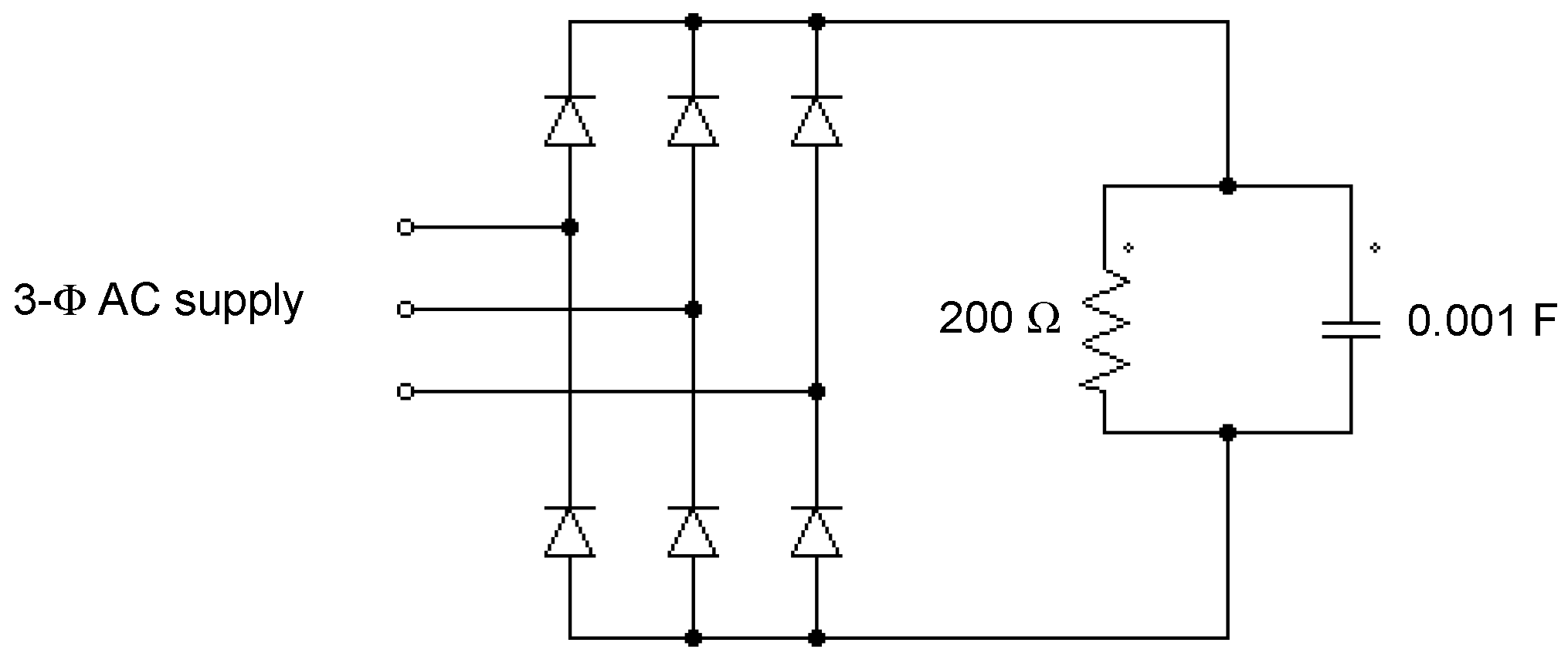
6. Investigated Schemes of SAPFs with FSTPI and SSTPI Using PSIM

6.1. Hardware Modeling in PSIM

This paper utilized PSIM hardware simulation and design software to study and investigate the FSTPI-based SAPF. The power circuit of the system is illustrated in Figure 8. It is composed of the following three main parts: AC supply including grid impedance, non-linear load (3-Φ uncontrolled rectified feeding R-L load), and the SAPF formed by the FSTPI scheme, including a DC bus capacitor.
The closed-loop control unit of the DC link voltage of the SAPF, including the reference current generation of the AC grid, is shown in Figure 9, while the corresponding SAPF reference currents’ generation and current controllers are illustrated in Figure 10. In this paper, the individual current controller is based on a PI controller and SPWM unit to generate the switching signals of the power transistors.
Both units of Figure 9 and Figure 10 are designed and developed in PSIM to operate with both types of inverters, SSTPI and FSTPI, as the paper performs a comparison between both SAPF schemes. Accordingly, in the upper part of Figure 9, the signal label (Isa_ref) is the reference grid current of phase A when the SSTPI scheme is utilized. Similarly in Figure 10, the signal labels (S1 and S4) represent the generated switching signals of the first arm of the SSTPI. This means that the operation of the FSTPI needs only four switching signals (S3, S6, S5, and S2), as illustrated in the lower part of Figure 10. The gains of the PI controllers are determined as explained in the next sub-section.

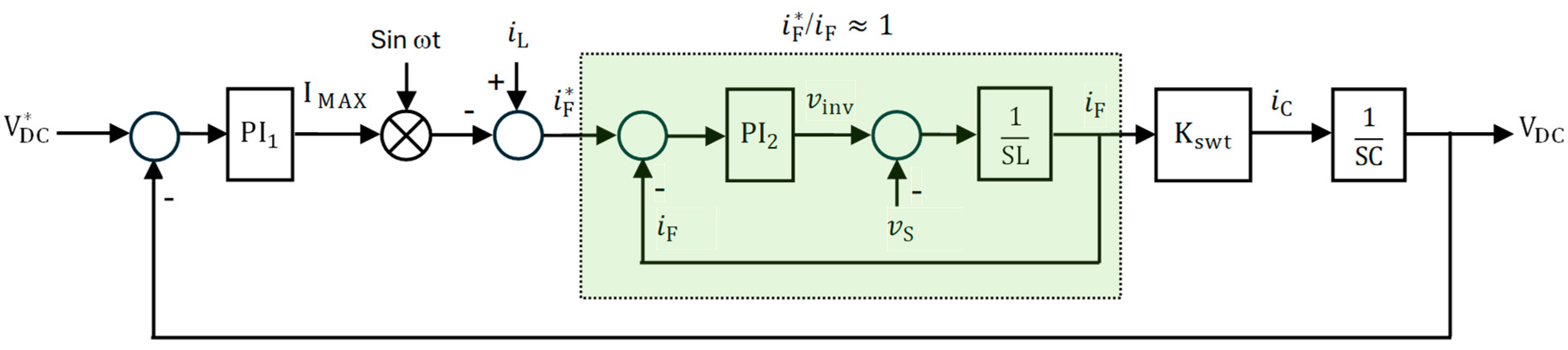
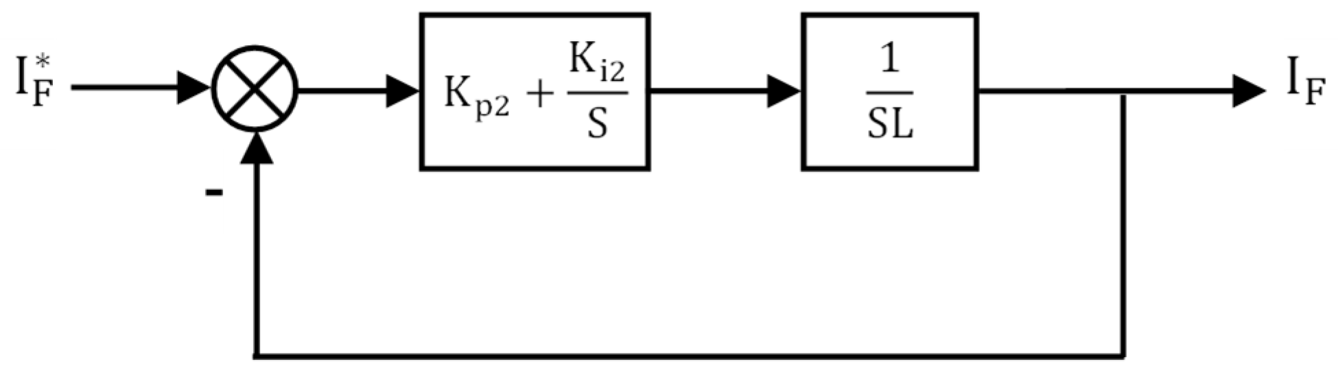
6.2. Design of PI Controllers

From Figure 9 and Figure 10, it can be indicated that the SAPF system has two control loops, a DC link voltage control loop (outer loop) and SAPF currents control loop (inner loop). A block diagram of the SAPF control system is illustrated in Figure 11. The system has the following two main controllers: a DC link voltage controller and SAPF current controllers. In the case of the FSTPI, the SAPF has two similar current controllers (to control the two phases’ currents i F b and i F c ), while in the case of the SSTPI, the SAPF has three similar controllers (to control the three phase currents i F a , i F b , and i F c ). In general, several types of controllers can be employed to regulate both the outer and inner control loops. Conducting a comparative study of different types of controllers to determine which type is the best is outside of the scope of this paper.
a. Outer control loop (voltage control loop):
As a control system, the simplified voltage control loop of the SAPF is shown in Figure 12. Since the VSI operates at a high switching frequency, the filter currents ( i F a , i F b , and i F c ) are almost equal to the magnitudes of their reference values ( i F a * , i F b * , i F c * ) , respectively. Therefore, it can be assumed that the transfer function of the closed-loop current controller ( i F * / i F ) is almost unity [32]. Kswt represents the inverter switching function to correlate the DC link current with the filter currents.
The transfer function of the PI voltage controller is given by Equation (9), as follows:
G p i 1 ( S ) = K p 1 + K i 1 S
Accordingly, the closed-loop transfer function will have the following formula:
T v S = S K p 1 + K i 1 C S 2 + S K p 1 + K i 1  
The gains Kp1 and Ki1 can be computed by comparing the characteristic equation of T v S with the standard form and solving for proper values of ζ 1 and ω n 1 .
Thus,
K p 1 = 2 ζ 1 ω n 1 C
K i 1 = C ω n 1 2
Thus, choose suitable values of ζ 1 and t s or ω n 1 to obtain the numerical values of Kp1 and Ki1. E.g., the damping ratio ζ 1 can be set to a value between 0.5 and 0.7, while the natural frequency ω n 1 can be selected based on the rise time or the settling time.
The numerical values of Kp1 and Ki1 obtained based on the previous method can be considered as good initial estimates for these gains. They can be tuned either manually or by applying any evolutionary search algorithms to achieve the optimum desired response (see Appendix A for complete derivation).
b. Inner control loop (current control loop):
The inner current control loop is shown in Figure 13. The output is the maximum value of the grid current. Several types of current controllers can be utilized such that the actual grid currents track and follow their reference values. The commonly used method is an ON–OFF current controller with a hysteresis band. However, the resultant switching frequency is not constant. In this paper, a PI controller and current controller are utilized for two reasons. Firstly, to obtain a fixed switching frequency. Secondly, to be able to make a fair comparison between the FSTPI and SSTPI schemes operating at the same switching frequency and in the same operating conditions (supply voltage and loading conditions).
Similarly, the closed-loop transfer function will have the following formula:
T i S = S K p 1 + K i 1 L S 2 + S K p 1 + K i 1
Comparing the characteristic equation of T i S with the standard form and solving for proper values of ζ 2 and ω n 2 yields the following formulas for Kp2 and Ki2:
K p 2 = 2 ζ 2 ω n 2 L
K i 2 = L ω n 2 2
Hence, choose suitable values of ζ 2 and t s 2 or ω n 2 to obtain the numerical values of Kp2 and Ki2. E.g., the damping ratio ( ζ ) can be set to a value between 0.5 and 0.7, while the natural frequency ω n 2 can be selected based on the rise time or the settling time. As mentioned before for the voltage control loop, the numerical values of Kp2 and Ki2 obtained based on the previous approach can be considered as good initial estimates that can be tuned either manually or by applying any evolutionary search algorithms to achieve a satisfactory response. Detailed derivations of the previous equations are presented in Appendix A.

6.3. Simulation Parameters

The simulation parameters of the developed PSIM programs of the investigated SAPF scheme are summarized in Table 1. The switching technique incorporated with the current controller is SPWM operating at a switching frequency of 10.02 kHz, which yields an odd frequency ratio of 167.

7. Obtained Results and Discussions

This section presents some simulation results of the SAPF driven by both the FSTPI and SSTPI under different loading conditions. The conducted study includes a quantitative analysis of the obtained results. A comparison between both schemes is made as well. The investigated nonlinear loads are as follows: (1) a three-phase diode bridge rectifier feeding a highly inductive load; (2) a three-phase diode bridge rectifier feeding a capacitive load to assess the system under a highly distorted waveform; and (3) three single-phase unbalanced non-linear loads formed by three single-phase diode bridge rectifiers loaded with unequal capacitive loads.

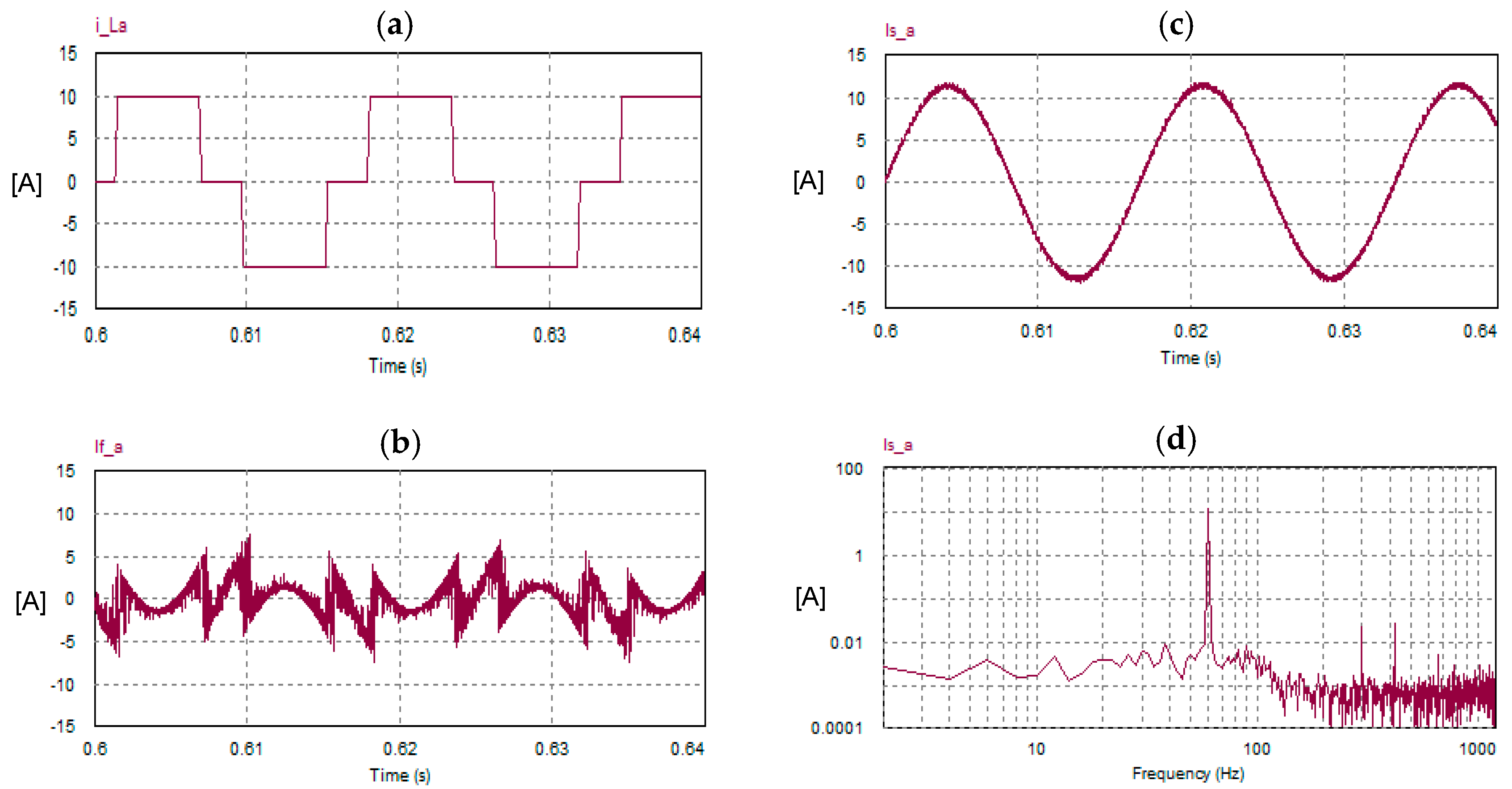
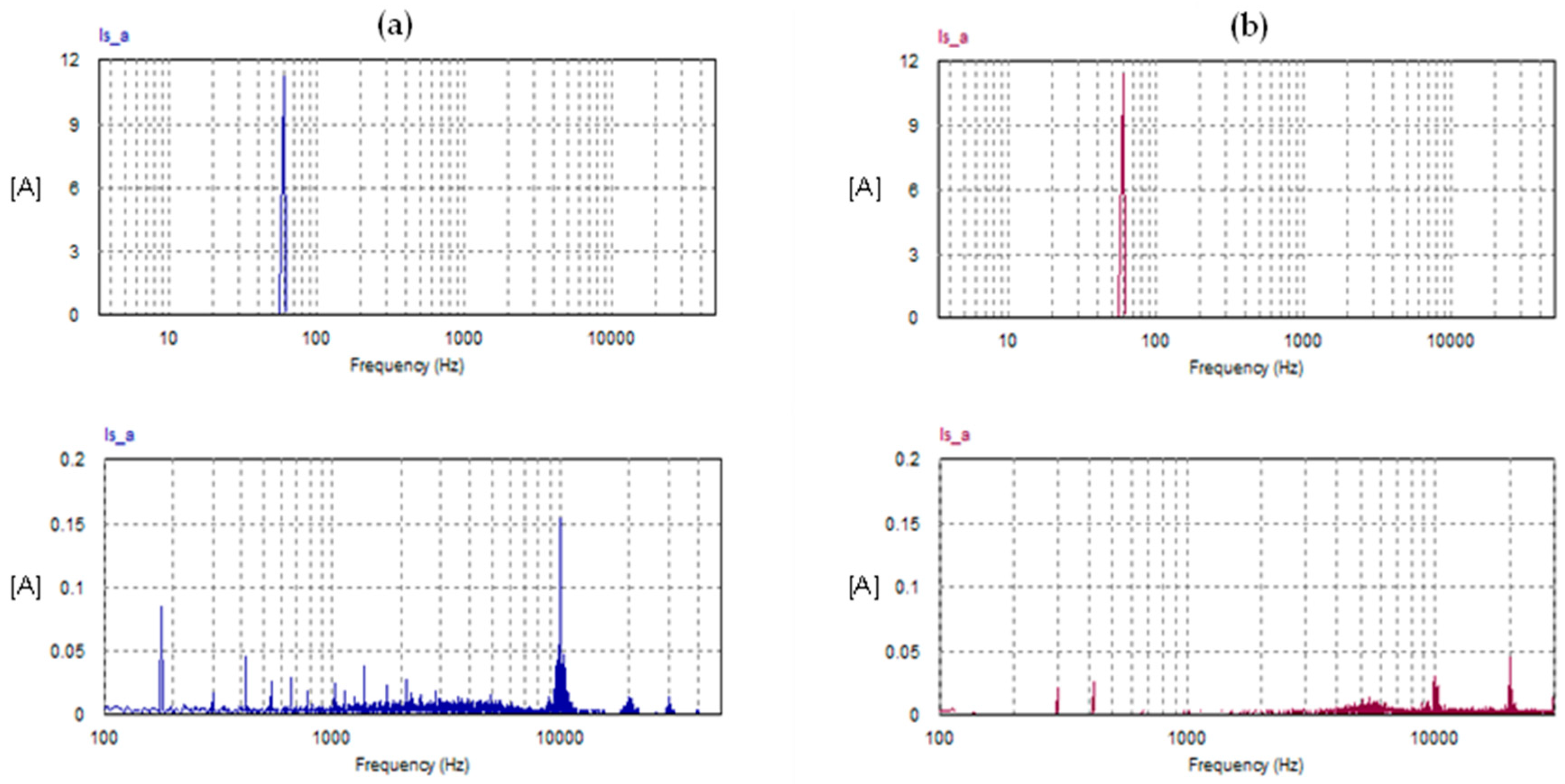
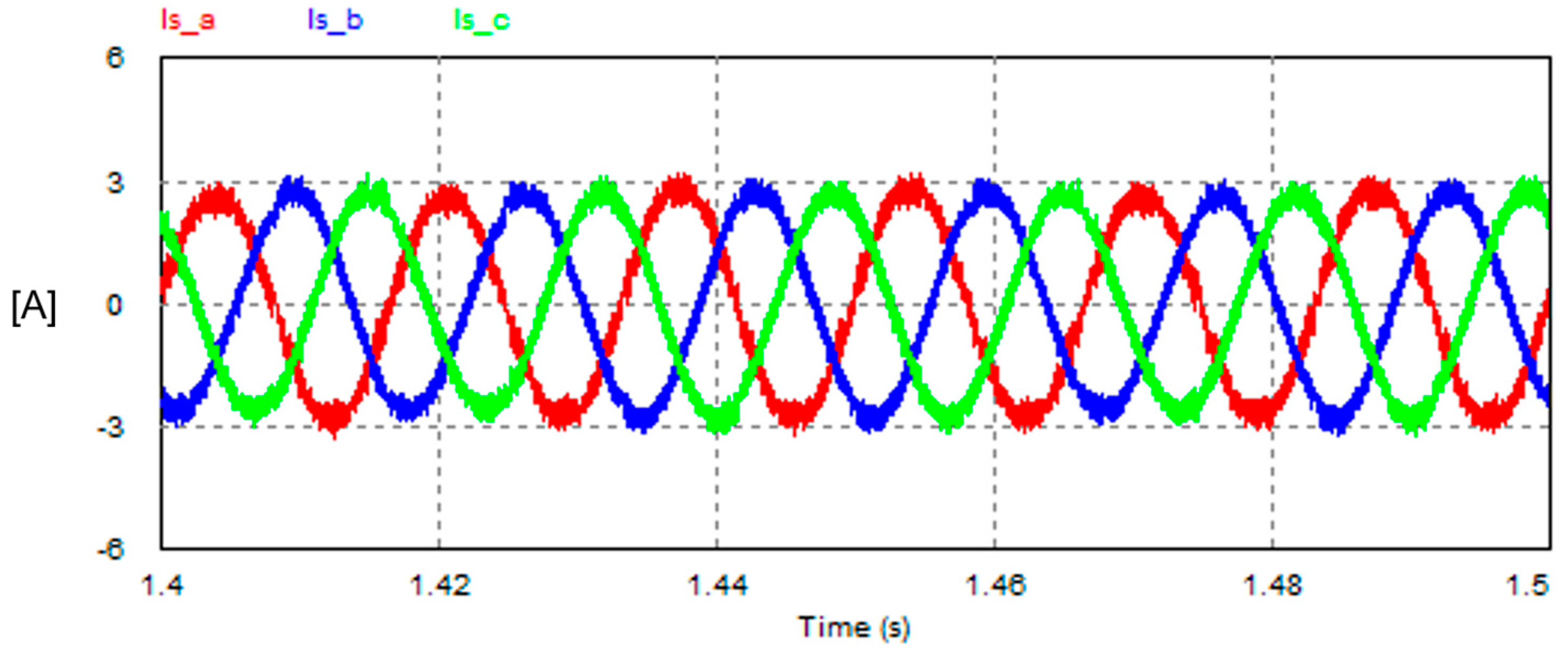
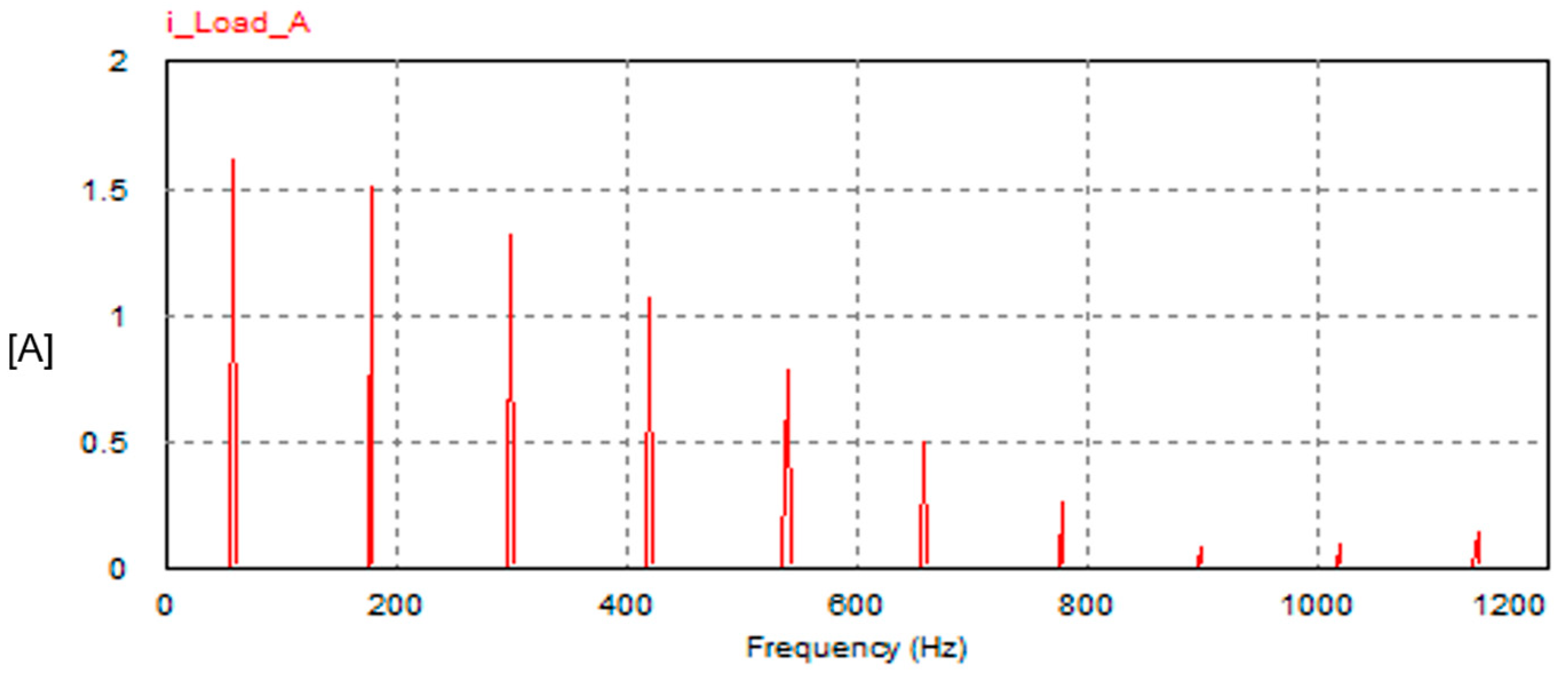
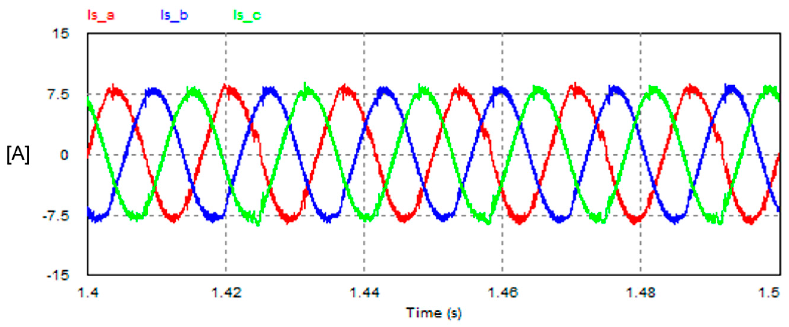
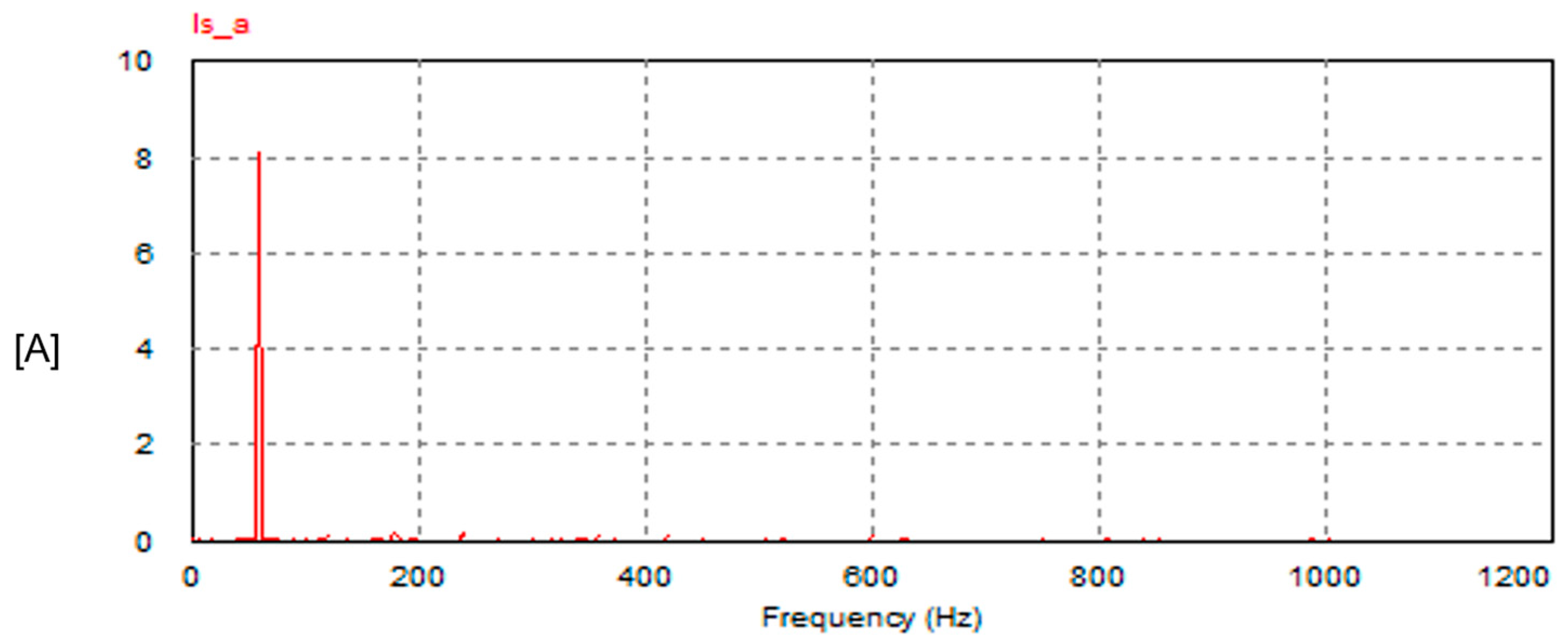
7.1. (Nonlinear Load): 3-Φ Diode Bridge Rectifier Feeding a Highly Inductive Load

a. SAPF with FSTPI Scheme.
The performance of the SAPF operated with the FSTPI is illustrated in Figure 14, where the nonlinear load current of the phase a ( i L a ) is depicted in Figure 14a. The corresponding injected filter current ( i F a ) is drawn in Figure 14b, while the resultant waveform of the supply current ( i s a ) and its harmonic spectrum are shown in Figure 14c,d, respectively. The obtained results indicate that the SAPF driven by the FSTPI operates properly and is effective in improving the current drawn from the AC supply. The harmonic spectrum contains odd harmonics (3, 5, 7…) with negligible magnitudes compared with the fundamental component (60 Hz). The low-order harmonic (third order of 180 Hz) has a magnitude of 0.68% of the fundamental component.
b. SAPF with SSTPI Scheme.
The performance of the SAPF operated with the conventional SSTPI is illustrated in Figure 15, where the nonlinear load current of the phase a ( i L a ) is depicted in Figure 15a. The corresponding injected filter current ( i F a ) is drawn in Figure 15b, while the resultant waveform of the supply current ( i s a ) and its harmonic spectrum are shown in Figure 15c,d, respectively.
The obtained results indicate that the SAPF driven by the FSTPI is competitive compared to the conventional SAPF scheme driven by the SSTPI. However, the SSTPI provides a relatively superior performance in terms of a lower THD and harmonic content, as explained later in the comparison part (Section 7.3).
c. Comparison with SSTPI Scheme.
Qualitative and quantitative assessments of both SAPFs are made to evaluate their performances and determine to which degree the proposed SAPF with the FSTPI scheme is successful and competitive compared to the conventional scheme.
In Figure 16, the three-phase supply currents of both schemes are depicted. The results demonstrate the sufficient quality of the current waveforms drawn from the grid under the FSTPI-based SAPF. The corresponding harmonic spectra are illustrated in Figure 17, where both schemes result in almost the same amplitude of the fundamental components. However, the AC grid currents under the SSTPI have better harmonic content compared with the FSTPI scheme.
The steady-state harmonic spectra of the DC link voltage with both schemes are illustrated in Figure 18. The results indicate the superior performance of the SSTPI in terms of lower harmonic content. In the case of the FSTPI scheme, the dominant low-order harmonic (LOH) pulsates at the grid frequency (60 Hz). Meanwhile, the dominant LOH in the case of the SSTPI scheme pulsates at six times the line frequency (360 Hz). Also, it can be observed that the harmonic spectrum of the DC link voltage with the FSTPI scheme has second, fourth, and fifth harmonics with relatively higher amplitudes compared with that of the SSTPI scheme.
Moreover, quantitative analysis is conducted to assess to which degree that the SAPF using the FSTPI scheme is successful and reliable. The comparison results are summarized in Table 2.
Owing to the results obtained with the quantitative analysis, the THD of the supply currents with the FSTP scheme is 3.2%, which is good. However, it is higher than that achieved by the SSTPI by 56%. Also, it is observed that the supply current with the FSTPI scheme contains a third harmonic component with a small amplitude, which is less than approximately 1% of the fundamental component (actually, it is 0.68%). The input PF is almost unity in both schemes (0.999). Although the DC bus voltages are well-regulated (controlled to the set point) in both schemes, the harmonic contents are in favor of the SSTPI scheme. E.g., when the load suddenly increases by 40% in a step change, both voltage controllers succeed in returning the DC bus voltage to the set point (600 V). The load recovery time is almost the same (in case of the SSTPI scheme it is 0.2 s, while in the FSTPI scheme it is 0.22 s), which is relatively higher than that of SSTPI scheme by 10%. The maximum voltage dip is almost the same as well. It is 1.5 V and 1.6 V in the SSTPI and FSTPI schemes, respectively.

7.2. (Highly Distorted Current): 3-Φ Diode Bridge Rectifier Loaded with a Capacitive Load

Discontinuous load currents with spikes, such as the case of the 3-Φ diode bridge rectifier loaded with a capacitive load, result in highly distorted current waveforms to be drawn from the AC mains. This type of load is challenging for any SAPF system. Therefore, such a challenging operating condition is investigated in this paper. The investigated nonlinear load is shown in Figure 19, where R is 200 Ω and C is 1 mF. Waveforms of the AC supply currents and harmonic spectra (before and after compensation) are presented.
Figure 20 illustrates the highly distorted currents drawn from the AC mains due to the 3-Φ diode bridge rectifier loaded with a capacitive load. The corresponding harmonic spectrum of the phase current is plotted in Figure 21. The dominant low-order harmonics are odd 5th, 7th, 11th, and 13th components with considerable amplitudes (no triplen). Moreover, the computed THD of the supply current is 125%. Meanwhile, the input PF is 0.624. This type of loading condition is challenging for SAPFs.
The SAPF using the FSTPI scheme succeeds in improving the waveforms of the currents drawn from the AC mains, as illustrated in Figure 22 and Figure 23. The resultant three-phase currents drawn from the AC supply are extremely improved. The computed THD is 9%. Meanwhile, the input PF improves to 0.99. This also can be indicated from the corresponding harmonic spectrum of the supply current isa depicted in Figure 23. The harmonic spectra of the supply current isa before and after applying the SAPF are shown in Figure 21 and Figure 23, respectively.
The obtained results illustrated in Figure 22 and Figure 23 indicate that the SAPF using the FSTPI scheme is efficient in compensating for the highly distorted current waveform, resulting in accepted THD levels and improved harmonic contents. The undesired dominant low order-harmonics are extremely attenuated.

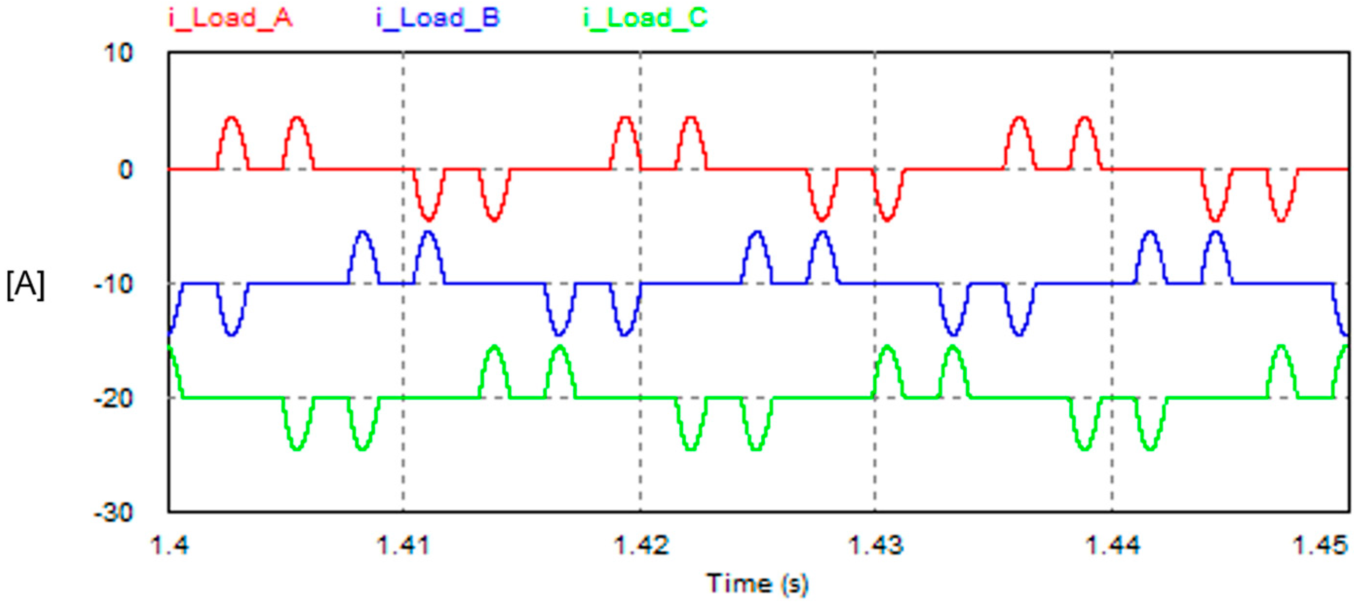
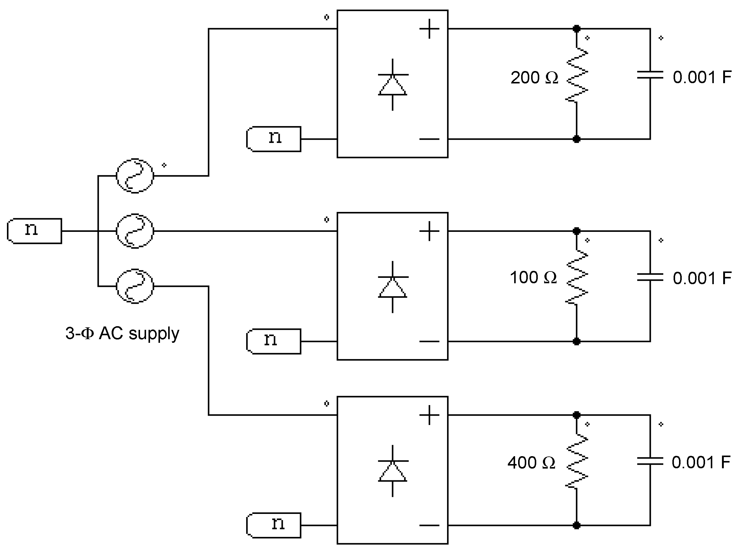
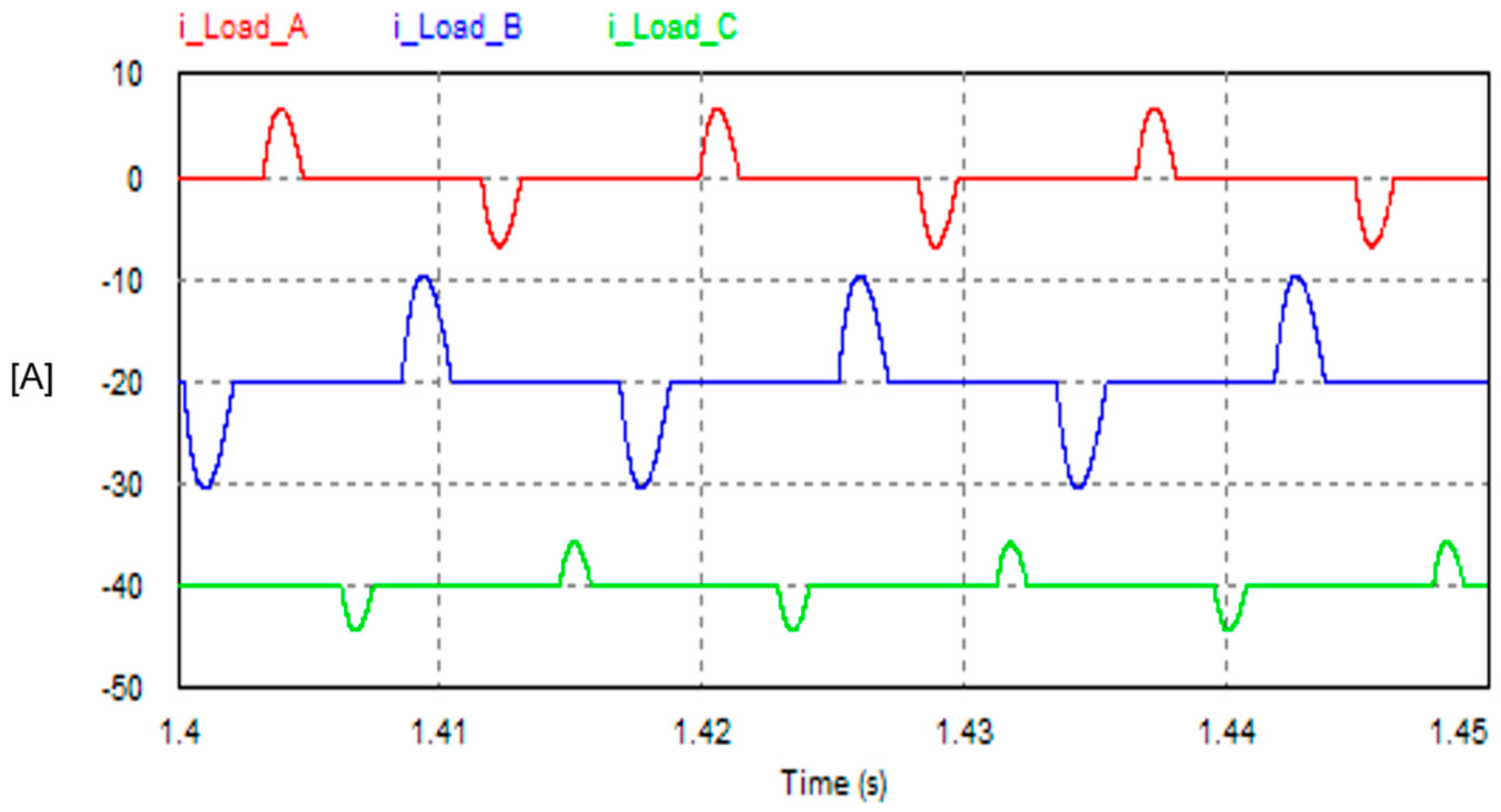
7.3. (Unbalanced Non-Linear Load): Three 1-Φ Diode Bridge Rectifiers Loaded with Unequal Capacitive Loads

The operation of the SAPF with the FSTPI scheme is tested under an unbalanced load condition. The load is also a nonlinear type. Three single-phase diode rectifiers feeding an unequal capacitive load are used to produce such unbalanced loading conditions, as illustrated in Figure 24. Practically, this case occurs in the real operation of many electronic appliances that employ old-fashioned power electronic converters (diode bridge rectifiers with smoothing capacitors). Figure 25 illustrates the currents drawn from the AC mains under unbalanced loading condition. The corresponding harmonic spectrum of the phase current isa is plotted in Figure 26. The dominant low-order harmonics are odd 3rd, 5th, 7th, 9th, 11th, and 13th components with considerable amplitudes. The computed THD of the supply current ias is 153%. Meanwhile, the input PF is 0.544. Such an unbalanced nonlinear load is also challenging to the operation of SAPFs.
The results obtained with the SAPF using the FSTPI scheme demonstrate the validity and effectiveness of the SAPF with the FSTPI scheme in alleviating unbalanced nonlinear loading conditions (see Figure 27 and Figure 28). The resultant three-phase currents drawn from the AC supply are significantly improved. Moreover, the FSTPI-based SAPF not only improves the waveforms of the supply currents, but also improves the input PF. The resultant THD of the supply current is extremely improved to a good value (6.2%). Meanwhile, the input PF is raised to 0.99. In addition, the undesired dominant low-order harmonics of the supply current isa are extremely attenuated, as indicated in Figure 28. The harmonic spectra of the supply current isa before and after applying the SAPF are shown in Figure 26 and Figure 28, respectively.

8. Conclusions

The paper presents a shunt active power filter (SAPF) using a four-switch three phase inverter (FSTPI) as an economic SAPF scheme. The FSTPI-based SAPF is studied under different nonlinear loading conditions, including a highly inductive load, highly distorted load, and unbalanced load. Also, the performance of the SAPF with the FSTPI topology is compared with the conventional SSTPI counterpart. Qualitative and quantitative analyses are carried out as well. The obtained results indicate the validity and effectiveness of the FSTPI scheme to be utilized in implementing SAPFs. The main findings are summarized in the following points:
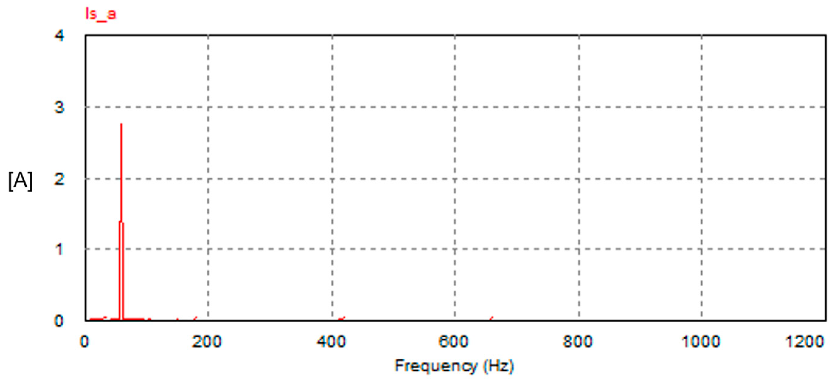
  • The total harmonic distortion (THD) of the grid current with the FSTPI scheme is 3.2%, while with the SSTPI scheme, it is 2.05%. Thus, the THD with the FSTPI is higher by 56%.
  • The amplitude of the fifth-order harmonic in the supply current does not exceed 1% of the fundamental component in both schemes. In the FSTPI, the ratio (I5/I1) is 0.66%, while the corresponding ratio in the SSTPI is 0.18%.
  • The input power factor (PF) in both schemes is almost unity (0.99).
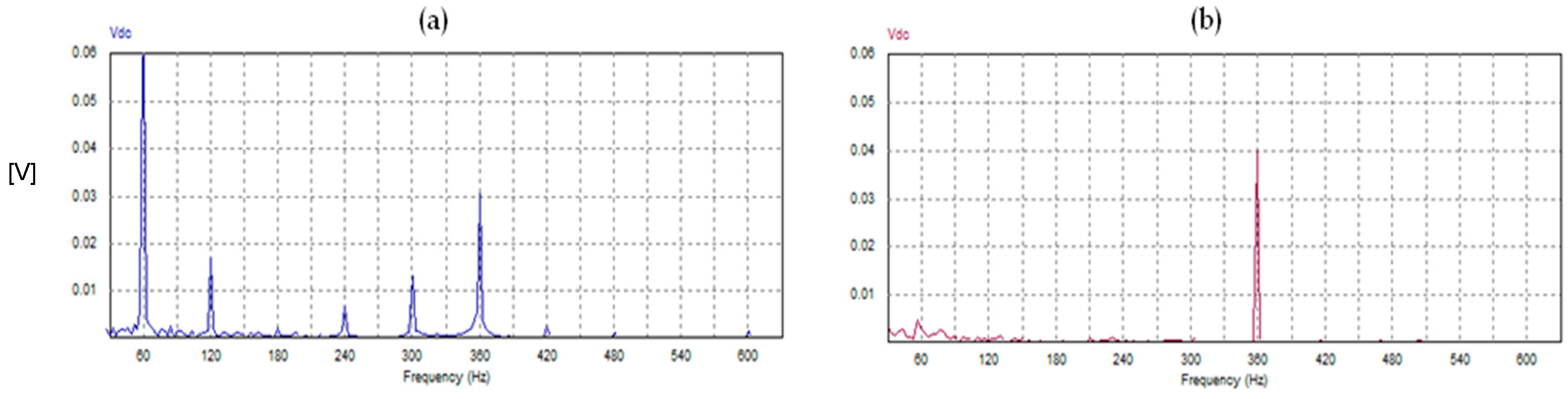
  • Both schemes of SAPFs produce the same average value of the DC link voltage, which is well-regulated to the desired set point (600 V) thanks to the PI voltage controllers of the outer voltage control loops. However, in the case of the FSTPI scheme, the dominant low-order harmonic of the DC link voltage pulsates at the supply frequency (60 Hz). Meanwhile in the case of the SSTPI, the dominant low-order harmonic of the DC link voltage pulsates at a rate six times the supply frequency (360 Hz).
  • The operation of the FSTPI-based SAPF is reliable and effective under highly distorted loading conditions. After compensation, the THD of the grid currents is extremely improved from 125% to 9%, meanwhile the PF is improved from 0.624 to 0.99.
  • The SAPF using the FSTPI is effective in compensating for the unbalanced nonlinear loading condition whose current waveform is highly distorted. The THD improves from 153% to 6.2%, meanwhile the PF improves from 0.544 to 0.99.
  • Compared with the SSTPI scheme, the proposed SAPF with the FSTPI scheme provides a reduction in the number of power transistors, freewheeling diodes, and auxiliary driver/isolation circuits by 33.33%. Moreover, the number of Hall effect current and voltage transducers that are needed to implement the SAPF with the FSTPI is reduced by the same amount (33%), which reduces the overall capital cost of the SAPF system.
  • The FSTPI scheme requires an additional two capacitors instead of two power semiconductor switches. Fortunately, the price of power capacitors is less than the price of power transistors, especially if their type is SiC.
  • The FSTPI scheme provides a reduction in conduction power losses of 33% for the same inverter current compared with its SSTPI counterpart.
  • Compared with the SSTPI scheme, the FSTPI suffers from an increase in switching power losses by 15.4% when both inverters operate at the same PWM switching frequency and the same inverter output voltage.
  • Although the conventional SAPF scheme with the SSTPI provides a relatively superior performance in terms of AC currents drawn from the grid with a lower THD and a lower harmonic content of the DC link voltage, the SAPF based on the FSTPI is considered to be competitive with the conventional SAPF scheme in terms of the reduced number of power semiconductor devices and transducers needed to implement the overall system.
  • The satisfactory performance achieved by the SAPFs with the FSTPI scheme makes the FSTPI scheme feasible and applicable when price reduction and fabricating economic SAPFs are of major concern.

Funding

This research received no funding.

Data Availability Statement

The original contributions presented in this study are included in the article. Further inquiries can be directed to the corresponding author(s).

Conflicts of Interest

The author declares no conflicts of interest.

Nomenclature

Abbreviations
APFActive power filter
FSTPI, B4Four-switch three-phase inverter
FFTFast Fourier transform
FO-PIDFractional-order PID
IGBTInsulated gate bipolar transistor
LOHLow-order harmonic
MOSFETMetal–oxide field-effect transistor
THDTotal harmonic distortion
PCCPoint of common coupling
PFPower factor
PLLPhase-locked loop
PIDProportional–integral–derivative
PWMPulse width modulation
SAPFShunt active power filter
SCRSilicon controlled rectifier
SPWMSinusoidal PWM
SiCSilicon Carbide
SSTPI, B6Six-switch three-phase inverter
SVMSpace vector modulation
VSIVoltage source inverter
WBGWide band gap
Symbols
i f a , i f b   ,   i f c Reference filter currents
i s a ,   i s b , i s c Reference supply (grid) currents
i L a , i L b , i L c Instantaneous values of the load currents
i L a 1 , i L b 1 , i L c 1 Instantaneous values of the 1st harmonic of the nonlinear load currents
I M A X * Peak value of the reference supply current
V D C * Reference DC link voltage
V D C Instantaneous value of DC link voltage
S1, S3, S5, S4, S6, S2Switching signals of the six transistors of SSTPI
S3, S5, S6, S2Switching signals of the four transistors of FSTPI
C1, C2Capacitors of the 1st branch of FSTPI
CDC link capacitor of SAPFs
L f Inductance of the inductor connected to the output of the SAPF
L s Inductance of the AC supply (grid inductance)
v s AC supply voltage
KswtSwitching function of the inverter
G p i 1 S , G p i 2 ( S ) Transfer functions of PI controllers of the voltage and current loops, respectively
G v S Open-loop gain function of the voltage control loop
G i S Open-loop gain function of the current control loop
T v ( S ) Closed-loop transfer function of the voltage control loop
T i ( S ) Closed-loop transfer function of the current control loop
K p 1 , K p 2 Proportional gains of the voltage and current controllers, respectively
K i 1 , K i 2 Integral gains the voltage and current controllers, respectively
ζ 1 ,   ζ 2 Damping ratios of voltage and current control loops, respectively
t s 1 , t s 2 Settling times of voltage and current control loops, respectively
ω n 1 , ω n 2 Natural frequencies of voltage and current control loops, respectively
ω Supply radian frequency

Appendix A

Appendix A.1. Derivation of PI Controller’s Gains of DC Voltage Control Loop

The transfer function of the PI voltage controller is given by Equation (A1), as follows:
G p i 1 ( S ) = K p 1 + K i 1 S = S K p 1 + K i 1 S
The open-loop gain function is given by Equation (A2), as follows:
G v S = G p i 1 S S C = S K p 1 + K i 1 S 2 C
Thus, the closed-loop transfer function of the voltage control loop is given by Equation (A3), as follows:
T v ( S ) = G v S 1 + G v S   H ( S )
where H(S) is 1 for unity feedback. Accordingly, the closed-loop transfer function will have the following formula:
T v S = S K p 1 + K i 1 C S 2   1 + S K p 1 + K i 1 C S 2   = S K p 1 + K i 1 C S 2 + S K p 1 + K i 1  
The gains Kp1 and Ki1 can be computed by comparing the characteristic equation of T v S with the standard form given by Equation (A5) and solving for proper values of ζ 1 and ω n 1 .
The standard form of characteristic equation is given by the following:
( S 2 + 2 ζ 1 ω n 1 S + ω n 1 2 = 0 )
Accordingly, the following relations are yielded:
2 ζ 1 ω n 1 = K p 1 C
ω n 1 2 = K i 1 C
Thus,
K p 1 = 2 ζ 1 ω n 1 C
K i 1 = C ω n 1 2

Appendix A.2. Derivation of PI Controller’s Gains of Inner Current Control Loop

G p i 2 ( S ) = K p 2 + K i 2 S =   S K p 2 + K i 2   S
The open-loop gain function is given by Equation (A11), as follows:
G i S = G p i 2 S S L = S K p 2 + K i 2 S 2 L
Therefore, the closed-loop transfer function of the current control loop is given by Equation (A12), as follows:
T i ( S ) = G i S 1 + G i S H ( S )
where H(S) is 1 for unity feedback. Accordingly, the closed-loop transfer function will have the following formula:
T i S = S K p 1 + K i 1 L S 2 1 + S K p 1 + K i 1 L S 2 = S K p 1 + K i 1 L S 2 + S K p 1 + K i 1
The gains Kp2 and Ki2 can be determined by comparing the characteristic equation of T i S with the standard form given by Equation (A14) and solving for proper values of ζ 2 and ω n 2 .
The standard form of characteristic equation is given by the following:
( S 2 + 2 ζ 2 ω n 2 S + ω n 2 2 = 0 )
Accordingly, the following relations are yielded:
2 ζ 2 ω n 2 = K p 2 L
ω n 2 2 = K i 2 L
Thus,
K p 2 = 2 ζ 2 ω n 2 L
K i 2 = L ω n 2 2

Appendix B

Comparative Analysis of SAPFs Using FSTPI and SSTPI Schemes

Table A1. Comparison between Both SAPF schemes.
ItemSSTPIFSTPI
Number of devicesTransistors and freewheeling diodes64
Isolation and driving circuits64
Hall effect current transducers 32
Hall effect voltage transducers
(for DC link voltage measurement)
11
Phase-locked loop (PLL) or Hall effect voltage transducers
(for unity gain signal synchronized with the AC grid voltage)
32
Capacitors (DC link and one branch of the inverter power circuit)13
Inverter output
voltage
Normalized line–line or line–neutral (at the same DC link voltage)1 1 3 = 0.577
Normalized required DC link voltage (for the same inverter output voltage1 3 = 1.732
Power lossesNormalized conduction losses
(for the same inverter load current)
10.666
Normalized switching losses
(for the same inverter output voltage and current and at the same PWM switching frequency)
1 4 6 3 = 1.154
Normalized total power losses1 ( 0.666 + 1.154 ) 2   = 0.91
Power quality Input PF0.990.99
Best achieved THD of AC grid current (at the same switching frequency, sampling time, passive filtering components)2%3%
Table A2. Percentage of saving/additional costs of FSTPI compared with SSTPI scheme.
ItemDescriptionPercentage
Saving in the devicesTransistors and freewheeling diodes33.3%
Isolation and driving circuits33.3%
Hall effect current transducers 33%
Phase-locked loop (PLL) or Hall effect voltage transducers
(for unity gain signal synchronized with the AC grid voltage)
33.3%
Additional cost of capacitorsTwo capacitors of one arm
(branch of no power transistors)
200%
Undesired reduction
in the inverter output voltage
For the same DC link voltage 42.3 %
Required additional increase in DC link voltageFor the same inverter output voltage73.2%
Reduction (saving)
in conduction power losses
For the same load current33.3%
Increasing in switching power lossesAt the same PWM switching frequency and for the same inverter output voltage and current 15.4 %
Saving in overall power lossesFor the same operating conditions 9 %

References

  1. Wu, Z.; Xu, G.; Zhu, W.; Sheng, G. The Stability Analysis and Control Strategies of Multi-paralleled SAPFs: A Comprehensive Overview. IEEE Trans. Power Electron. 2024, 39, 7444–7457. [Google Scholar] [CrossRef]
  2. Torabi Jafrodi, S.; Ghanbari, M.; Mahmoudian, M.; Najafi, A.M.G.; Rodrigues, E.; Pouresmaeil, E. A Novel Control Strategy to Active Power Filter with Load Voltage Support Considering Current Harmonic Compensation. Appl. Sci. 2020, 10, 1664. [Google Scholar] [CrossRef]
  3. Buła, D.; Michalak, J.; Zygmanowski, M.; Adrikowski, T.; Jarek, G.; Jeleń, M. Control Strategy of 1 kV Hybrid Active Power Filter for Mining Applications. Energies 2021, 14, 4994. [Google Scholar] [CrossRef]
  4. Kukrer, O.; Komurcugil, H.; Guzman, R.; de Vicuna, L.G. A New Control Strategy for Three-Phase Shunt Active Power Filters Based on FIR Prediction. IEEE Trans. Ind. Electron. 2021, 68, 7702–7713. [Google Scholar] [CrossRef]
  5. Pichan, M.; Seyyedhosseini, M.; Hafezi, H. A New Dead Beat-Based Direct Power Control of Shunt Active Power Filter With Digital Implementation Delay Compensation. IEEE Access 2022, 10, 72866–72878. [Google Scholar] [CrossRef]
  6. Zhou, J.; Yuan, Y.; Dong, H. Adaptive DC-Link Voltage Control for Shunt Active Power Filters Based on Model Predictive Control. IEEE Access 2020, 8, 208348–208357. [Google Scholar] [CrossRef]
  7. Hoon, Y.; Zainuri, M.A.A.M.; Al-Ogaili, A.S.; Al-Masri, A.N.; Teh, J. Active Power Filtering Under Unbalanced and Distorted Grid Conditions Using Modular Fundamental Element Detection Technique. IEEE Access 2021, 9, 107502–107518. [Google Scholar] [CrossRef]
  8. Nie, X.; Liu, J. Current Reference Control for Shunt Active Power Filters Under Unbalanced and Distorted Supply Voltage Conditions. IEEE Access 2019, 7, 177048–177055. [Google Scholar] [CrossRef]
  9. Al-Gahtani, S.F.; Nelms, R.M. Performance of a Shunt Active Power Filter for Unbalanced Conditions Using Only Current Measurements. Energies 2021, 14, 397. [Google Scholar] [CrossRef]
  10. Kumar, R.; Bansal, H.O.; Gautam, A.R.; Mahela, O.P.; Khan, B. Experimental Investigations on Particle Swarm Optimization Based Control Algorithm for Shunt Active Power Filter to Enhance Electric Power Quality. IEEE Access 2022, 10, 54878–54890. [Google Scholar] [CrossRef]
  11. Muneer, V.; Biju, G.M.; Bhattacharya, A. Optimal Machine-Learning-Based Controller for Shunt Active Power Filter by Auto Machine Learning. IEEE J. Emerg. Sel. Top. Power Electron. 2023, 11, 3435–3444. [Google Scholar] [CrossRef]
  12. Gao, Y.; Li, X.; Zhang, W.; Hou, D.; Zheng, L. A Sliding Mode Control Strategy with Repetitive Sliding Surface for Shunt Active Power Filter with an LCLCL Filter. Energies 2020, 13, 1740. [Google Scholar] [CrossRef]
  13. de Rossiter Correa, M.B.; Jacobina, C.B.; da Silva, E.R.C.; Lima, A.M.N. A General PWM Strategy for Four-Switch Three-Phase Inverters. IEEE Trans. Power Electron. 2006, 21, 1618–1627. [Google Scholar] [CrossRef]
  14. Kim, G.-T.; Lipo, T.A. VSI-PWM rectifier/inverter system with a reduced switch count. IEEE Trans. Ind. Appl. 1996, 32, 1331–1337. [Google Scholar] [CrossRef]
  15. Jacobina, C.B.; da Silva, E.R.C.; Lima, A.M.N.; Ribeiro, R.L.A. Vector and scalar control of a four switch three phase inverter. In Proceedings of the IAS ’95. Conference Record of the 1995 IEEE Industry Applications Conference Thirtieth IAS Annual Meeting, Orlando, FL, USA, 8–12 October 1995; Volume 3, pp. 2422–2429. [Google Scholar] [CrossRef]
  16. Ledezma, E.; Munoz-Garcia, A.; Lipo, T.A. A dual three-phase drive system with a reduced switch count. In Proceedings of the Conference Record of 1998 IEEE Industry Applications Conference. Thirty-Third IAS Annual Meeting (Cat. No.98CH36242), St. Louis, MO, USA, 12–15 October 1998; Volume 1, pp. 781–788. [Google Scholar] [CrossRef]
  17. Liang, D.T.W. Novel modulation strategy for a four-switch three-phase inverter. In Proceedings of the Second International Conference on Power Electronics and Drive Systems, Singapore, 26–29 May 1997; Volume 2, pp. 817–822. [Google Scholar] [CrossRef]
  18. Correa, M.B.R.; Jacobina, C.B.; Lima, A.M.N.; Da Silva, E.R.C. A new approach to generate PWM patterns for four-switch three-phase inverters. In Proceedings of the 30th Annual IEEE Power Electronics Specialists Conference. Record. (Cat. No.99CH36321), Charleston, SC, USA, 1 July 1999; Volume 2, pp. 941–946. [Google Scholar] [CrossRef]
  19. Guo, F.; Qiao, J.; Jia, T.; Wang, L. Control strategy for three-phase four-switch active power filter based on positive sequence extraction in stationary coordinate fundamental reference frame. J. Phys. Conf. Ser. 2023, 2656, 012022. [Google Scholar] [CrossRef]
  20. Hasim, A.S.B.A.; Dardin, S.M.F.B.S.M.; Ibrahim, Z.B. Kalman Filters for Reference Current Generation in Shunt Active Power Filter (APF). In Kalman Filters–Theory for Advanced Applications; InTech: London, UK, 2018. [Google Scholar] [CrossRef]
  21. Chedjara, Z.; Massoum, A.; Wira, P.; Safa, A.; Gouichiche, A. A fast and robust reference current generation algorithm for three-phase shunt active power filter. Int. J. Power Electron. Drive Syst. 2021, 12, 121–129. [Google Scholar] [CrossRef]
  22. Chauhan, S.K.; Shah, M.C.; Tiwari, R.R.; Tekwani, P.N. Analysis, design and digital implementation of a shunt active power filter with different schemes of reference current generation. IET Power Electron. 2014, 7, 627–639. [Google Scholar] [CrossRef]
  23. Hasim, A.S.A.; Ibrahim, Z.; Talib, M.H.N.; Dardin, S.M.F.S.M. Three-Phase Reference Current Generator Employing with Kalman Filter for Shunt Active Power Filter. J. Electr. Eng. Technol. 2017, 12, 151–160. [Google Scholar] [CrossRef]
  24. Abdusalam, M.; Poure, P.; Karimi, S.; Saadate, S. New digital reference current generation for shunt active power filter under distorted voltage conditions. Electr. Power Syst. Res. 2009, 79, 759–765. [Google Scholar] [CrossRef]
  25. IEEE Std. 519-2014; IEEE Recommended Practice and Requirements for Harmonic Control in Electric Power Systems. (Revision of IEEE Std 519-1992). IEEE: Piscataway, NJ, USA, 2014; pp. 1–29.
  26. IEEE. IEEE Application Guide for IEEE Standard 1547; IEEE Standard for Interconnecting Distributed Resources with Electric Power Systems; IEEE: Piscataway, NJ, USA, 2009; Volume 1547, pp. 1–207. [Google Scholar]
  27. IEEE Standard 1459-2010; IEEE Standard Definitions for the Measurement of Electric Power Quantities Under Sinusoidal, Nonsinusoidal, Balanced, or Unbalanced Conditions. IEEE: Piscataway, NJ, USA, 2010; pp. 1–40.
  28. Bosch, S.; Staiger, J.; Steinhart, H. Predictive Current Control for an Active Power Filter With LCL-Filter. IEEE Trans. Ind. Electron. 2018, 65, 4943–4952. [Google Scholar] [CrossRef]
  29. Kashif, M.; Hossain, M.J.; Fernandez, E.; Taghizadeh, S.; Sharma, V.; Ali, S.N.; Irshad, U.B. A Fast Time-Domain Current Harmonic Extraction Algorithm for Power Quality Improvement Using Three-Phase Active Power Filter. IEEE Access 2020, 8, 103539–103549. [Google Scholar] [CrossRef]
  30. Jana, S.; Srinivas, S. A Computationally Efficient Harmonic Extraction Algorithm for Grid Applications. IEEE Trans. Power Deliv. 2022, 37, 146–154. [Google Scholar] [CrossRef]
  31. Liu, H.; Hu, H.; Chen, H.; Zhang, L.; Xing, Y. Fast and flexible selective harmonic extraction methods based on the generalized discrete fourier transform. IEEE Trans. Power Electron. 2018, 33, 3484–3496. [Google Scholar] [CrossRef]
  32. Imam, A.A.; Sreerama Kumar, R.; Al-Turki, Y.A. Modeling and Simulation of a PI Controlled Shunt Active Power Filter for Power Quality Enhancement Based on P-Q Theory. Electronics 2020, 9, 637. [Google Scholar] [CrossRef]
Figure 1. Block diagram of the shunt active power filter system.
Electricity 06 00016 g001
Figure 2. Circuit diagram of a typical SAPF system.
Electricity 06 00016 g002
Figure 3. Generation of reference grid currents from the closed-loop control of the DC link voltage.
Electricity 06 00016 g003
Figure 4. Generation of reference grid currents by computing the fundamental component of the load current.
Electricity 06 00016 g004
Figure 5. Possible current controllers for SAPF currents.
Electricity 06 00016 g005
Figure 6. Power circuit of a four-switch 3-Φ inverter (FSTPI).
Electricity 06 00016 g006
Figure 7. Simple current control of an FSTPI.
Electricity 06 00016 g007
Figure 8. Power circuit of the investigated FSTPI-based SAPF in PSIM.
Electricity 06 00016 g008
Figure 9. Closed-loop control unit of the DC link voltage developed in PSIM.
Electricity 06 00016 g009
Figure 10. SAPF reference currents’ generation and current controllers developed in PSIM.
Electricity 06 00016 g010
Figure 11. Voltage and current control loops of SAPF.
Electricity 06 00016 g011
Figure 12. Simplified DC voltage control loop of SAPF.
Electricity 06 00016 g012
Figure 13. Simplified inner current control loop of SAPF.
Electricity 06 00016 g013
Figure 14. Performance of SAPF using FSTPI scheme: (a) nonlinear load current iLa; (b) injected filter current iFa; (c) resultant supply current isa; and (d) harmonic spectrum of supply current isa.
Electricity 06 00016 g014
Figure 15. Performance of SAPF using SSTPI Scheme: (a) Nonlinear load current iLa; (b) injected filter current iFa; (c) resultant supply current isa; and (d) harmonic spectrum of supply current isa.
Electricity 06 00016 g015
Figure 16. 3-Φ supply currents (isa, isb, and isc) with both SAPF schemes: (a) FSTPI and (b) SSTPI.
Electricity 06 00016 g016
Figure 17. Harmonic spectrum of supply current isa with both SAPF schemes: (a) FSTPI and (b) SSTPI.
Electricity 06 00016 g017
Figure 18. Harmonic spectrum of the DC bus voltage VDC with both SAPF schemes: (a) FSTPI and (b) SSTPI.
Electricity 06 00016 g018
Figure 19. Highly distorted load formed by 3-Φ diode bridge feeding a capacitive load.
Electricity 06 00016 g019
Figure 20. Highly distorted load currents due to 3-Φ diode bridge rectifier loaded with a capacitive load.
Electricity 06 00016 g020
Figure 21. Harmonic spectrum of the highly distorted load current depicted in Figure 20.
Electricity 06 00016 g021
Figure 22. 3-Φ supply currents (isa, isb, and isc ) with SAPF using FSTPI scheme under highly distorted load current.
Electricity 06 00016 g022
Figure 23. Harmonic spectrum of AC supply current isa with SAPF using FSTPI scheme under highly distorted load current.
Electricity 06 00016 g023
Figure 24. Unbalanced nonlinear capacitive load formed by three 1-Φ diode bridges feeding unequal capacitive loads.
Electricity 06 00016 g024
Figure 25. Unbalanced supply currents due to unbalanced nonlinear capacitive load.
Electricity 06 00016 g025
Figure 26. Harmonic spectrum of the supply current isa depicted in Figure 25.
Electricity 06 00016 g026
Figure 27. 3-Φ supply currents (isa, isb, and isc) with SAPF using FSTPI scheme under unbalanced nonlinear loading condition.
Electricity 06 00016 g027
Figure 28. Harmonic spectrum of AC supply current isa with SAPF using FSTPI scheme under unbalanced nonlinear loading condition.
Electricity 06 00016 g028
Table 1. Simulation parameters.
ParameterValue
AC supply ( v s )3-Φ: 208 V/60 Hz
DC bus capacitor (C)4 mF
FSTPI capacitors (C1, C2)1 mF
Total inductance (L = Lf + Ls)4 mH
Switching strategySPWM
Switching frequency (FSWT)10.02 kHz
Solver time step5 μs
DC link voltage (VDC)600 V
Table 2. Performance Assessment of both SAPF schemes.
ItemParameterSAPF-SSTPISAPF-FSTPI
Supply Current
i s a
THD 2.05%3.2%
First Harmonic 11.2711.24 A
Third Harmonic0.0007 A0.077 A
I5/I10.18%0.66%
PF0.9990.999
DC link voltage V D C Minimum value599.96599.85
Maximum value600.06600.13
Dominant LOH61
First Harmonic 0.0027 V0.064 V
Second Harmonic0.0007 V0.017 V
Third Harmonic0.0005 V0.0024 V
Fourth Harmonic9.4 × 10−5 V0.0067 V
Fifth Harmonic 0.0002 V0.0131 V
Sixth Harmonic0.039V0.030 V
Disclaimer/Publisher’s Note: The statements, opinions and data contained in all publications are solely those of the individual author(s) and contributor(s) and not of MDPI and/or the editor(s). MDPI and/or the editor(s) disclaim responsibility for any injury to people or property resulting from any ideas, methods, instructions or products referred to in the content.

