

Design Techniques for Low-Power and Low-Voltage Bandgaps †


Abstract
:1. Introduction
2. Low-Voltage Bandgap Design
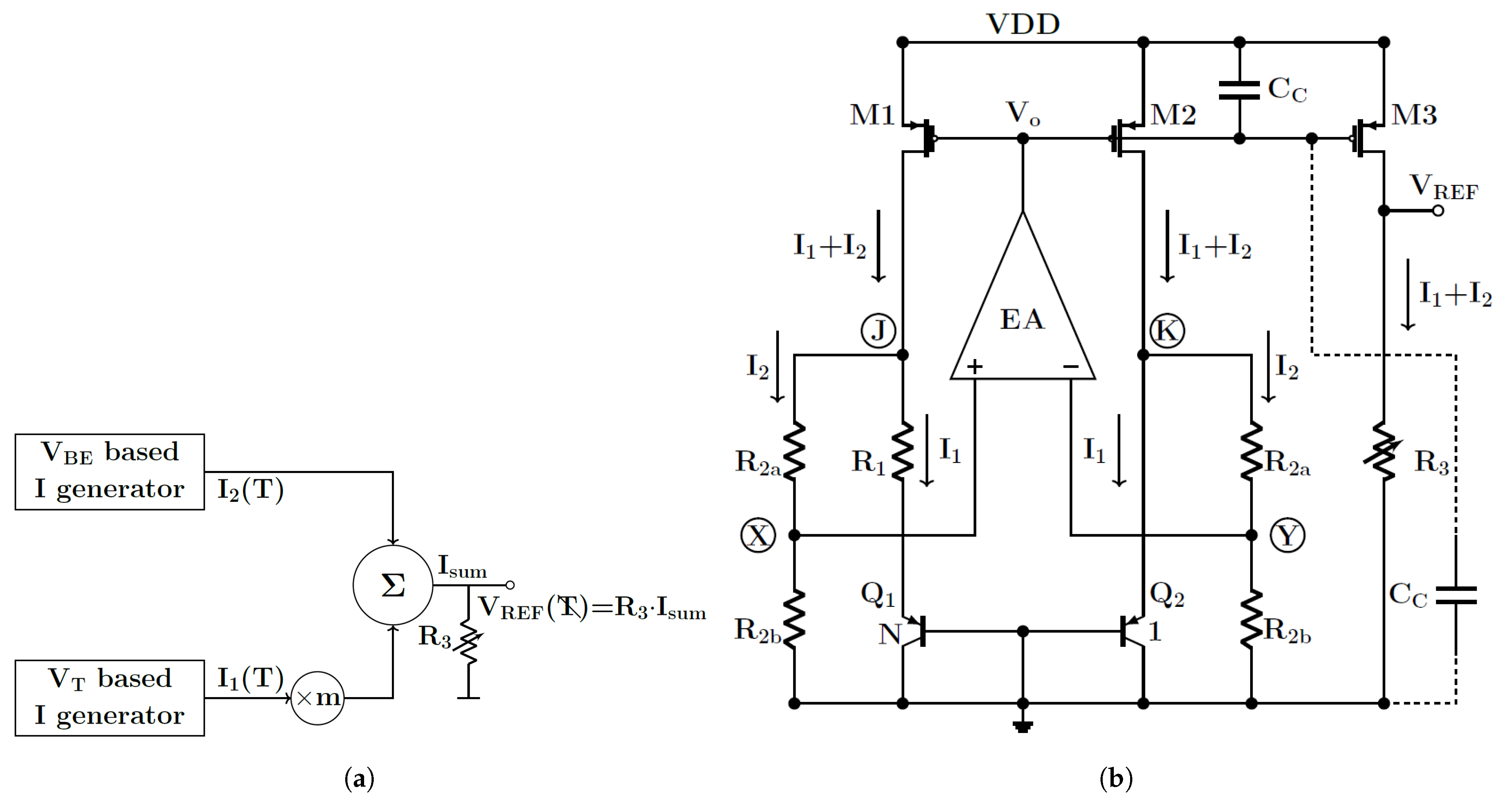
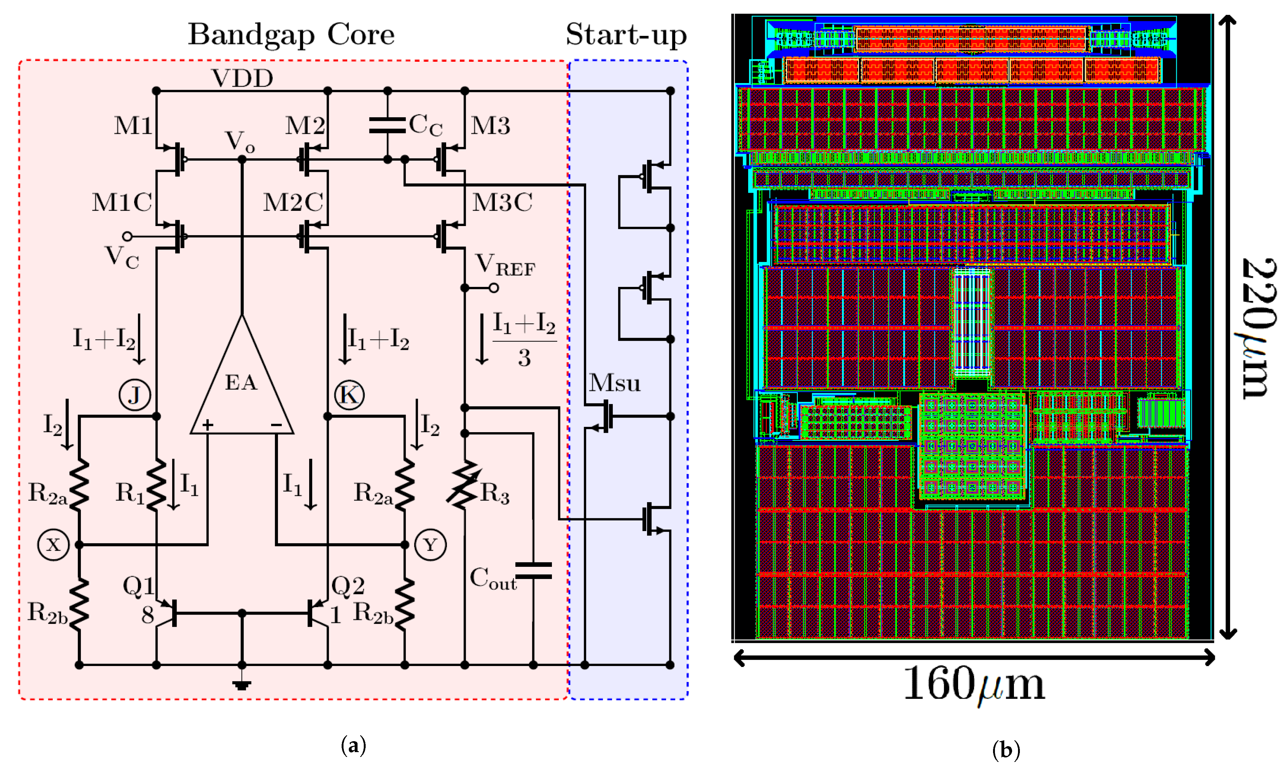
2.1. Bandgap Branches
2.2. Trimming Resistor
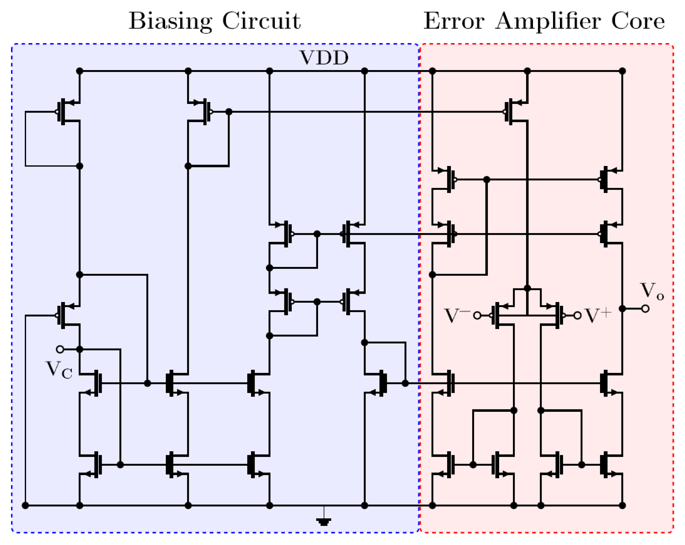
2.3. Error Amplifier
2.3.1. EA Bias
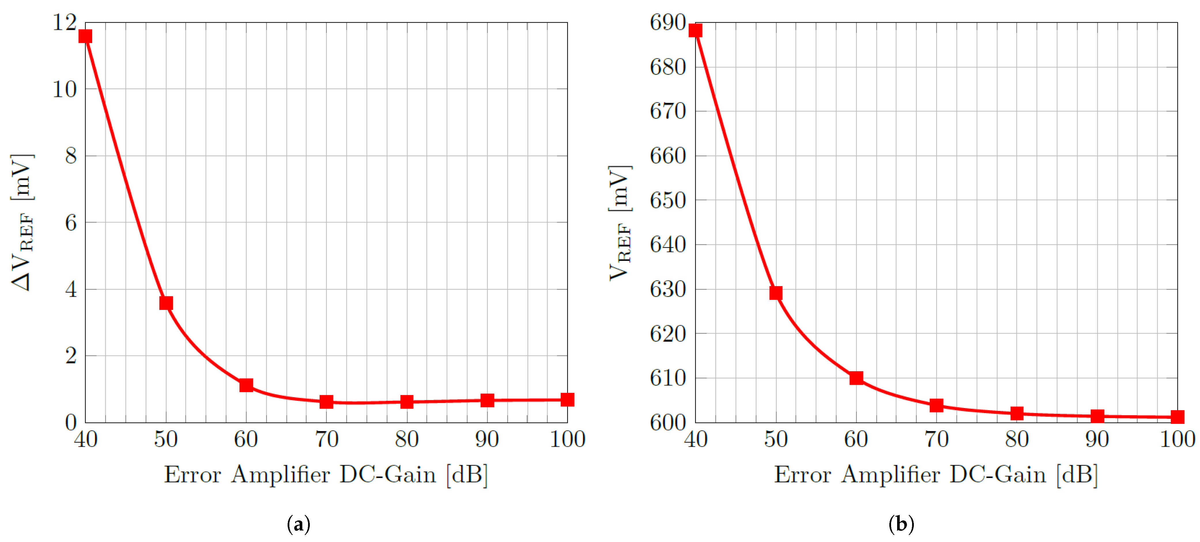
2.3.2. EA DC-Gain Specification
2.3.3. EA Offset Specification
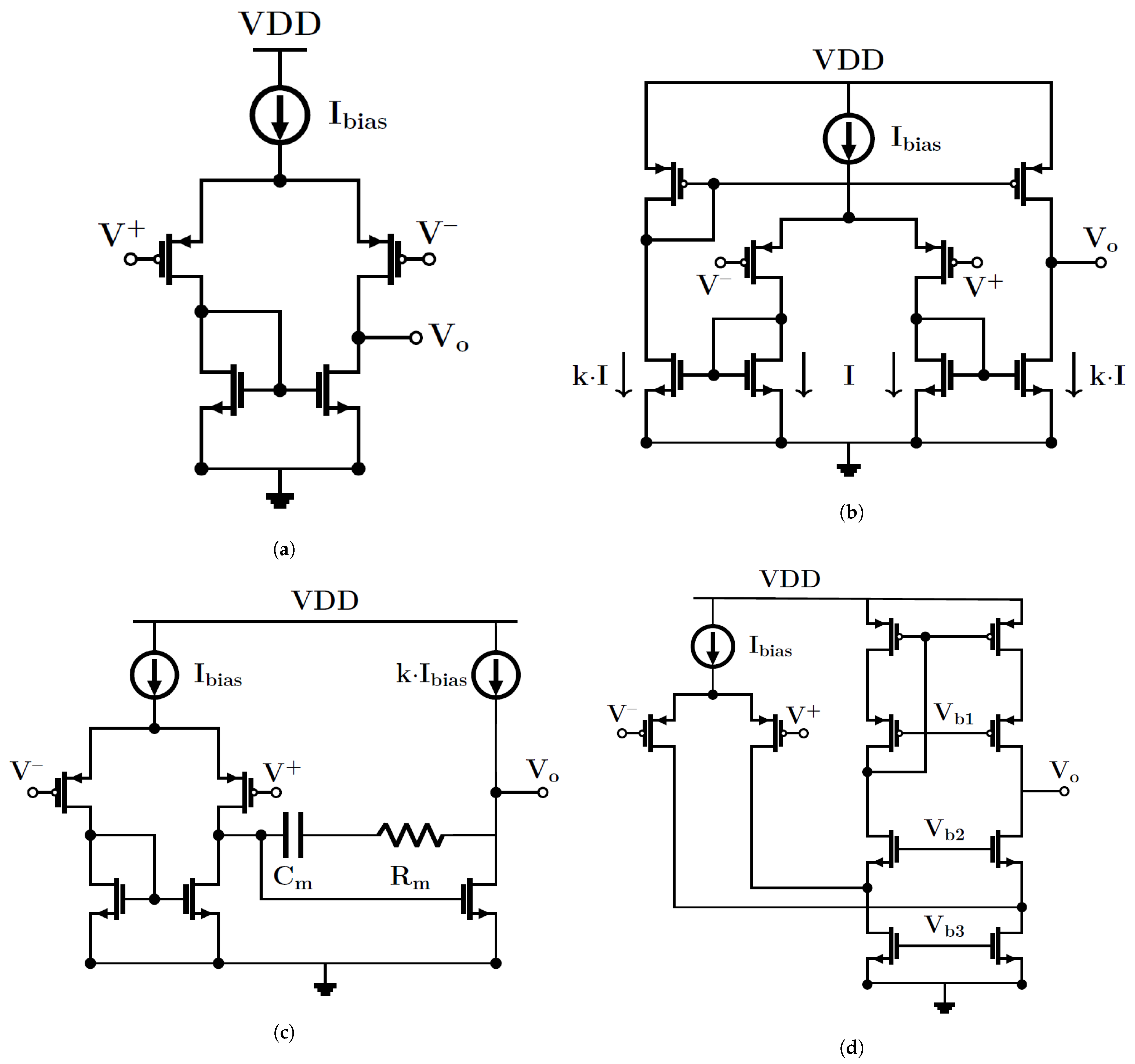
2.3.4. EA Topology
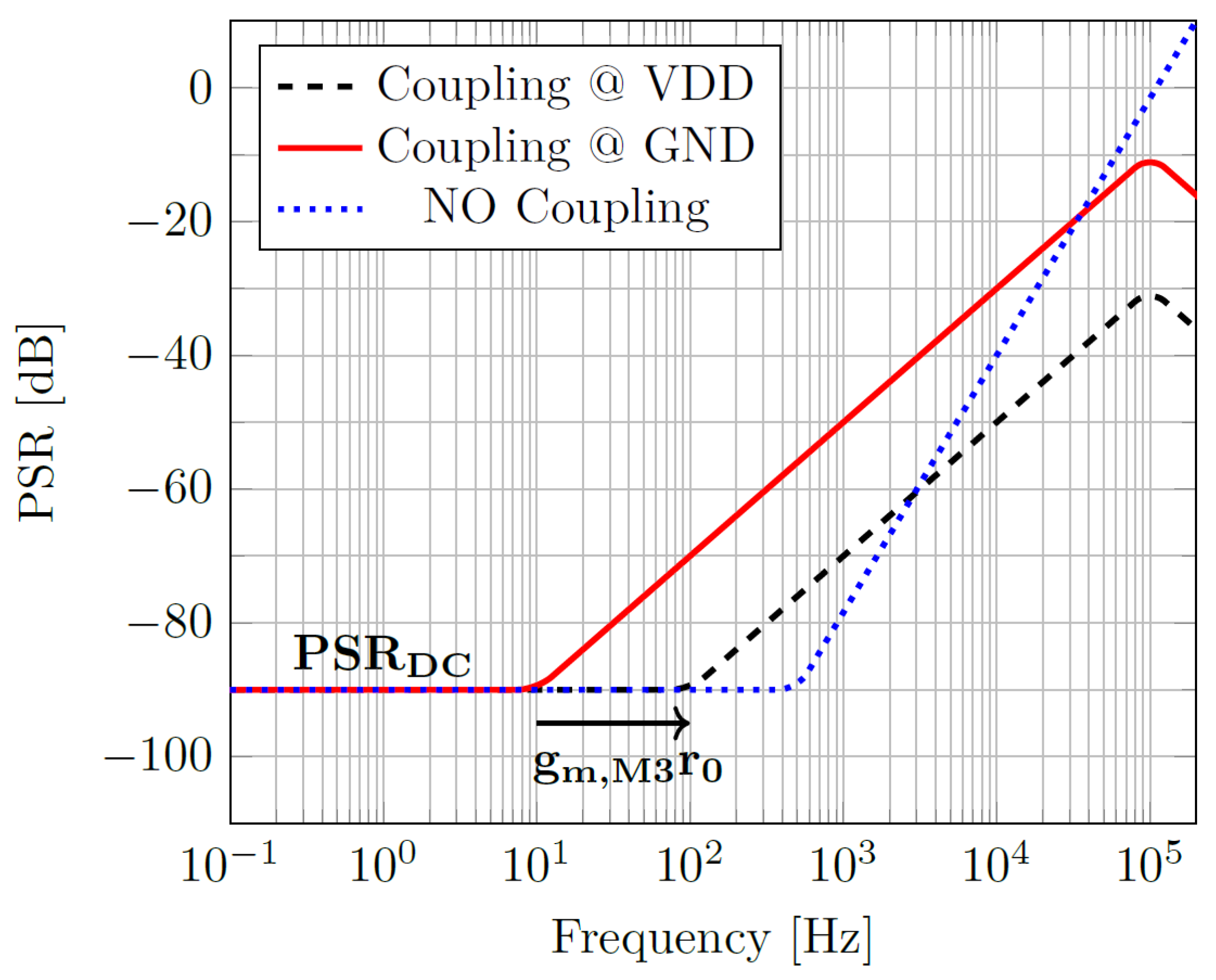
2.4. Power Supply Rejection
3. LV-LP BG Design in 65 nm Technology
3.1. Bandgap Branch Design
3.2. Error Amplifier Structure
3.3. Start-Up and Biasing Circuit
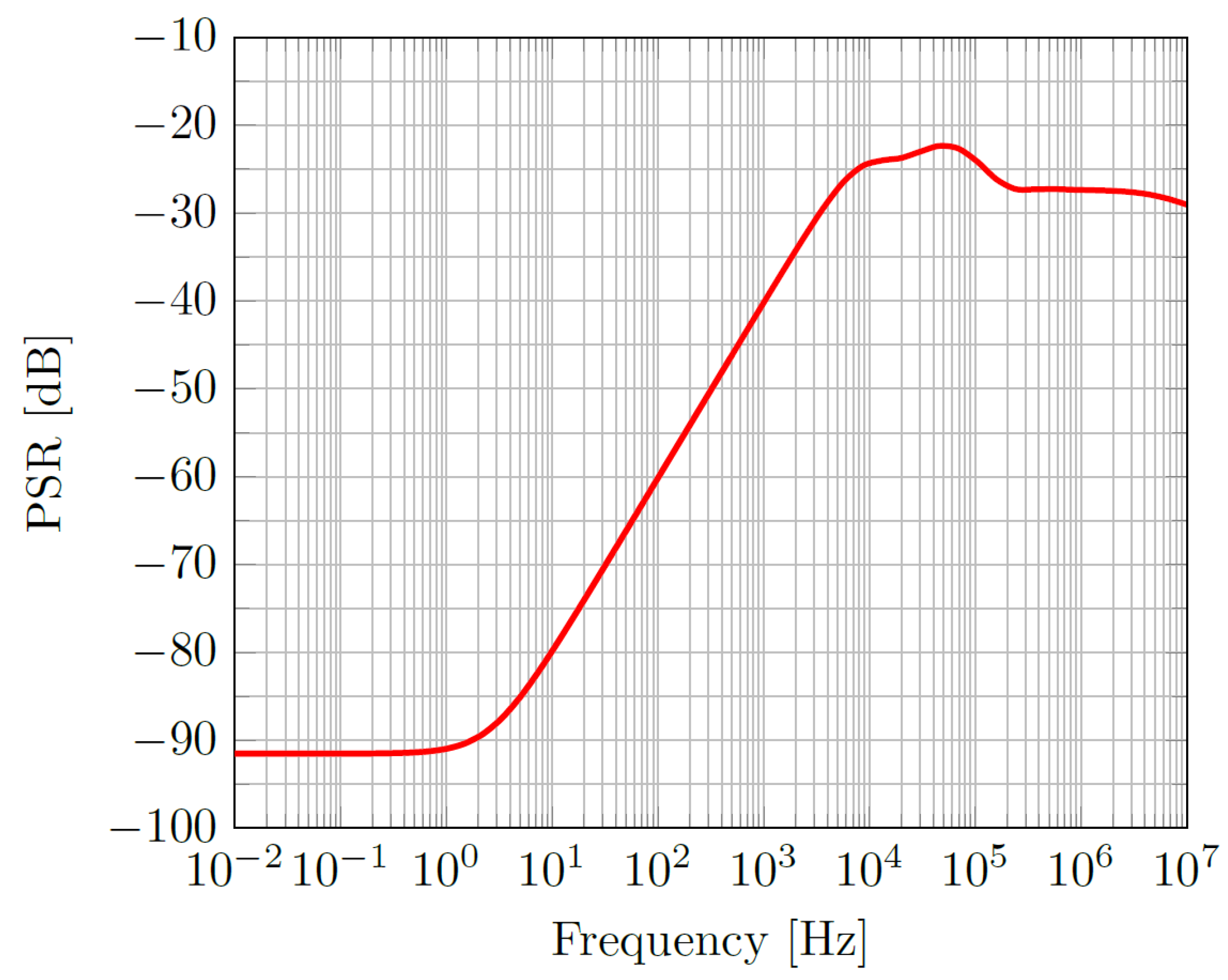
3.4. PSR Simulation
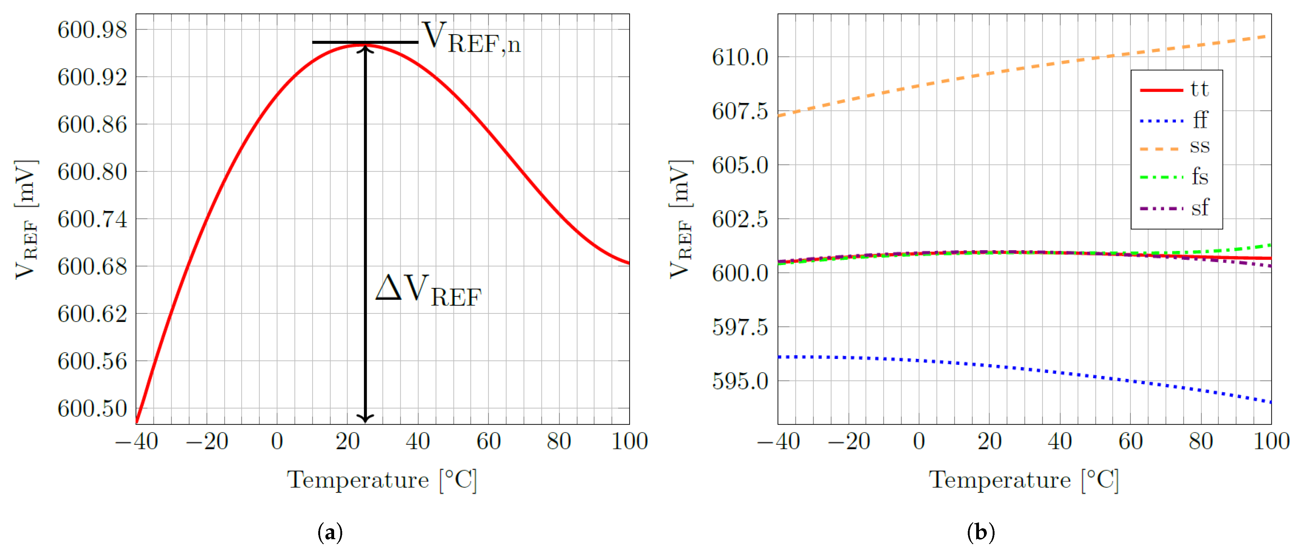
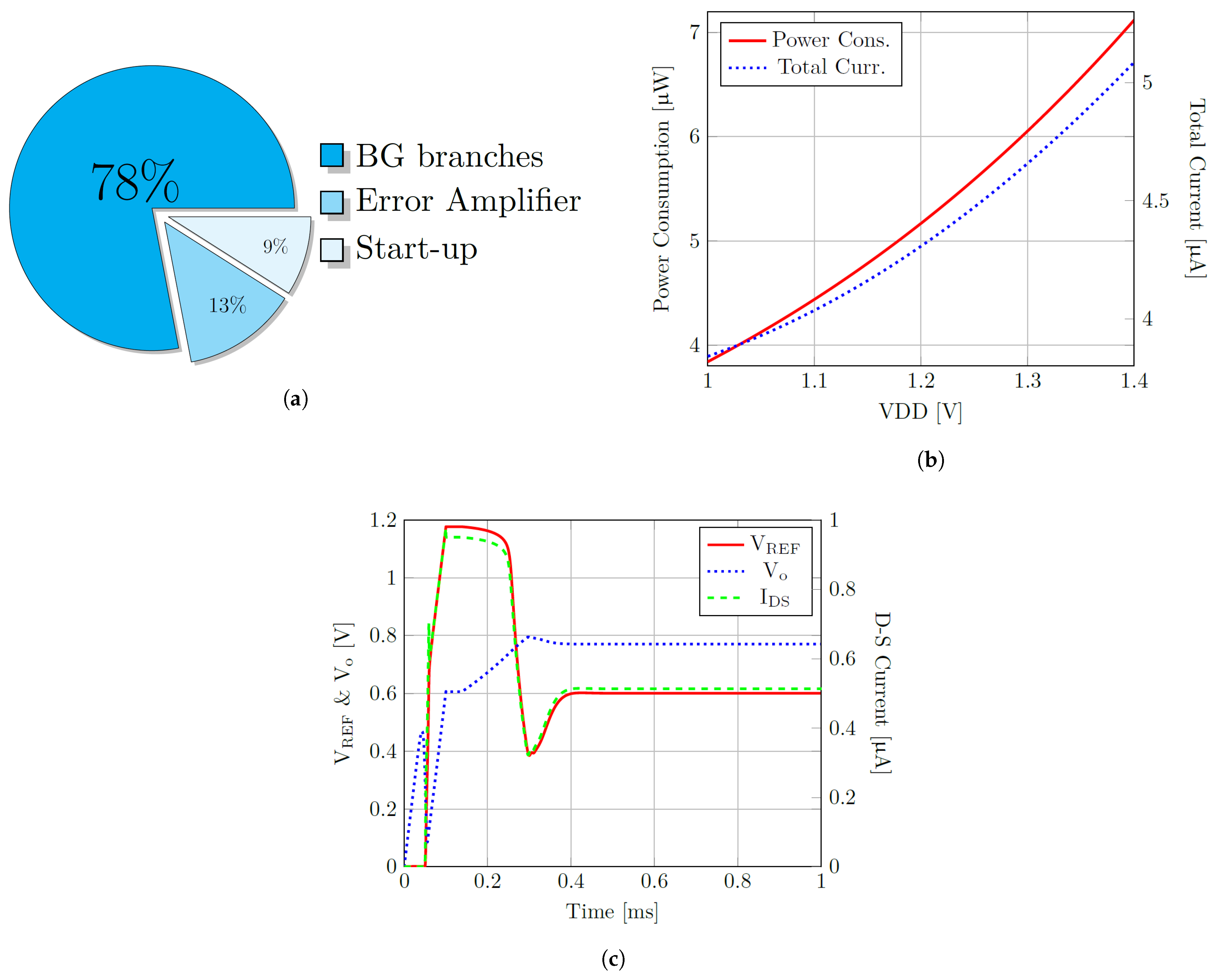
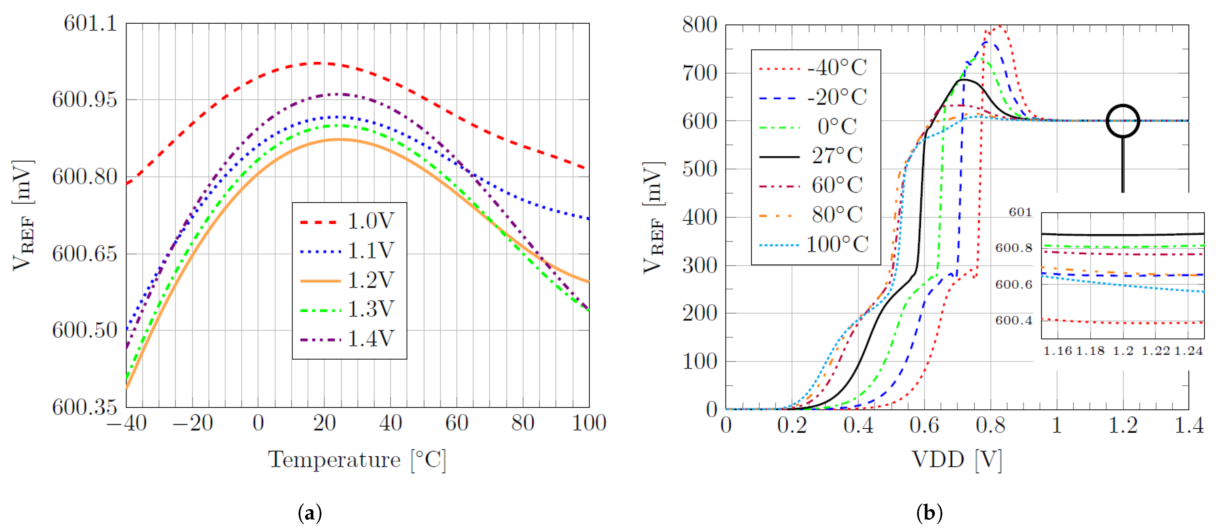
3.5. DC Simulation
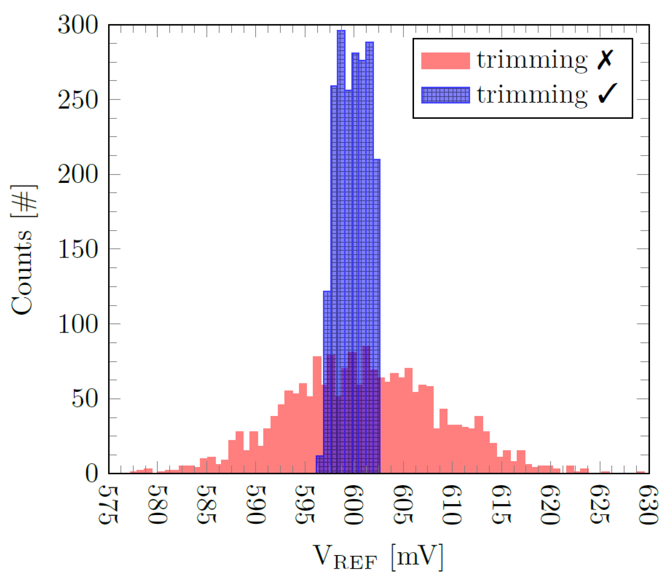
3.6. Monte Carlo Simulation
4. Conclusions
Author Contributions
Funding
Institutional Review Board Statement
Informed Consent Statement
Data Availability Statement
Conflicts of Interest
References
- Shrivastava, A.; Craig, K.; Roberts, N.E.; Wentzloff, D.D.; Calhoun, B.H. 5.4 A 32 nW bandgap reference voltage operational from 0.5 V supply for ultra-low power systems. In Proceedings of the 2015 IEEE International Solid-State Circuits Conference—(ISSCC) Digest of Technical Papers, San Francisco, CA, USA, 22–26 February 2015; pp. 1–3. [Google Scholar] [CrossRef]
- Longhitano, A.N.; del Cesta, F.; Bruschi, P.; Simmarano, R. A compact low-noise fully differential bandgap voltage reference with intrinsic noise filtering. In Proceedings of the 2014 10th Conference on Ph.D. Research in Microelectronics and Electronics (PRIME), Grenoble, France, 30 June–3 July 2014; pp. 1–4. [Google Scholar] [CrossRef]
- Banba, H.; Shiga, H.; Umezawa, A.; Miyaba, T.; Tanzawa, T.; Atsumi, S.; Sakui, K. ACMOS bandgap reference circuit with sub-1-V operation. IEEE J. Solid-State Circuits 1999, 34, 670–674. [Google Scholar] [CrossRef] [Green Version]
- Malcovati, P.; Maloberti, F.; Fiocchi, C.; Pruzzi, M. Curvature-compensated BiCMOS bandgap with 1-V supply voltage. IEEE J. Solid-State Circuits 2001, 36, 1076–1081. [Google Scholar] [CrossRef] [Green Version]
- Widlar, R.J. Low voltage techniques [for micropower operational amplifiers]. IEEE J. Solid-State Circuits 1978, 13, 838–846. [Google Scholar] [CrossRef]
- Cabrini, A.; De Sandre, G.; Gobbi, L.; Malcovati, P.; Pasotti, M.; Poles, M.; Rigoni, F.; Torelli, G. A 1 V, 26 /spl mu/W extended temperature range band-gap reference in 130-nm CMOS technology. In Proceedings of the 31st European Solid-State Circuits Conference, Grenoble, France, 2–16 September 2005; pp. 503–506. [Google Scholar] [CrossRef]
- Boni, A. Op-amps and startup circuits for CMOS bandgap references with near 1-V supply. IEEE J. Solid-State Circuits 2002, 37, 1339–1343. [Google Scholar] [CrossRef] [Green Version]
- Waltari, M.; Halonen, K. Reference voltage driver for low-voltage CMOS A/D converters. In Proceedings of the ICECS 2000, 7th IEEE International Conference on Electronics, Circuits and Systems (Cat. No.00EX445), Jounieh, Lebanon, 17–20 December 2000; pp. 28–31. [Google Scholar] [CrossRef]
- Leung, K.N.; Mok, P.K.T. A sub-1-V 15-ppm//spl deg/C CMOS bandgap voltage reference without requiring low threshold voltage device. IEEE J. Solid-State Circuits 2002, 37, 526–530. [Google Scholar] [CrossRef]
- Mok, P.K.T.; Leung, K.N. Design considerations of recent advanced low-voltage low-temperature-coefficient CMOS bandgap voltage reference. In Proceedings of the IEEE 2004 Custom Integrated Circuits Conference (IEEE Cat. No.04CH37571), Orlando, FL, USA, 6 October 2004; pp. 635–642. [Google Scholar] [CrossRef] [Green Version]
- Pelgrom, M.J.M.; Duinmaijer, A.C.J.; Welbers, A.P.G. Matching properties of MOS transistors. IEEE J. Solid-State Circuits 1989, 24, 1433–1439. [Google Scholar] [CrossRef]
- Colombo, D.M.; Wirth, G.I. Impact of Different Op-Amps in CMOS Bandgap References Implemented in 0.18 μM Technology. Available online: https://sbmicro.org.br/sforum-eventos/sforum2009/colombo.pdf (accessed on 6 July 2021).
- Wang, L.; Zhan, C.; Zhao, S.; Cai, C.; Liu, Y.; Huang, Q.; Li, G. Design of high-PSRR current-mode bandgap reference with improved frequency compensation. In Proceedings of the 2016 IEEE International Conference on Electron Devices and Solid-State Circuits (EDSSC), Hong Kong, China, 3–5 August 2016; pp. 142–149. [Google Scholar]
- Barteselli, E.; Sant, L.; Gaggl, R.; Baschirotto, A. A First Order-Curvature Compensation 5ppm/°C Low-Voltage & High PSR 65nm-CMOS Bandgap Reference with one-point 4-bits Trimming Resistor. In Proceedings of the 2021 Conference on Ph.D. Research in Microelectronics and Electronics (PRIME), Erfurt, Germany, 19–22 July 2021. [Google Scholar]
- Zhang, J.; Li, G.; Yan, B.; Luo, P.; Yang, Y.; Zhang, R.; Li, X. A bandgap reference in 65 nm CMOS. In Proceedings of the 2016 IEEE International Nanoelectronics Conference (INEC), Chengdu, China, 9–11 May 2016; pp. 1–2. [Google Scholar]
- Peng, K.; Xu, Y. Design of Low-Power Bandgap Voltage Reference for IoT RFID Communication. In Proceedings of the 2018 IEEE 3rd International Conference on Integrated Circuits and Microsystems (ICICM), Shanghai, China, 24–26 November 2018; pp. 345–348. [Google Scholar] [CrossRef]
- Yang, S.; Mak, P.; Martins, R.P. A 104 μW EMI-resisting bandgap voltage reference achieving −20 dB PSRR, and 5% DC shift under a 4 dBm EMI level. In Proceedings of the 2014 IEEE Asia Pacific Conference on Circuits and Systems (APCCAS), Ishigaki, Japan, 17–20 November 2014; pp. 57–60. [Google Scholar] [CrossRef]
- Chi-Wa, U.; Zeng, W.-L.; Law, M.-K.; Lam, C.-S.; Martins, R.P. A 0.5-V Supply, 36 nW Bandgap Reference With 42 ppm/°C Average Temperature Coefficient Within −40 °C to 120 °C. IEEE Trans. Circuits Syst. I Regul. Pap. 2020, 67, 3656–3669. [Google Scholar] [CrossRef]
- Lu, T.; Ker, M.; Zan, H. A 70 nW, 0.3 V temperature compensation voltage reference consisting of subthreshold MOSFETs in 65 nm CMOS technology. In Proceedings of the 2016 International Symposium on VLSI Design, Automation and Test (VLSI-DAT), Hsinchu, Taiwa, 25–27 April 2016; pp. 1–4. [Google Scholar]
- Li, X.; Kok, C.L.; Wu, C.D.; Siek, L.; Zhu, D.; Xiao, Z.K.; Lim, W.M.; Goh, W.L. A novel voltage reference with an improved folded cascode current mirror OpAmp dedicated for energy harvesting application. In Proceedings of the 2013 International SoC Design Conference (ISOCC), Busan, Korea, 17–19 November 2013; pp. 318–321. [Google Scholar]


| [13] S | [15] M | [16] S | [17] S | [18] M | [19] M | [20] M | This Work S | |
|---|---|---|---|---|---|---|---|---|
| 2016 | 2016 | 2018 | 2014 | 2020 | 2016 | 2013 | 2020 | |
| Proc. (nm) 1 | 180 | 65 | 65 | 65 | 65 | 65 | 65 | 65 |
| VDD (V) | 1.1–2.2 | 1.1–1.3 | 1.2 | N.A. | 0.5 | 0.3 | 0.6–1.2 | 1.0–1.4 |
| VREF,n (mV) | 800 | 466 | 730 | ∼441.5 | 495 | 168 | 435 | 600 |
| T. Range (°C) | −40∼125 | −55∼125 | −20∼100 | −45∼120 | −40∼120 | −20∼100 | −40∼125 | −40∼100 |
| P. Cons. (μW) | 19.8 | N.A. | N.A. | 104 | 0.036 | 0.07 | 0.22 | 5.2 |
| TC (ppm/°C) | 9 | 30.9 | 9.8 | 10.65 | 42 | 142 | 30 | 5 |
| PSR DC (dB) | −108 | −61 | −79 | −20.21 | −50 | N.A. | −38 | −91 |
| PSR 10 k (dB) | −68 | N.A. | ∼−30 | −20.21 | N.A. | N.A. | −27.5 | −24.8 |
| Area (mm2) | 0.04 | 0.5 * | N.A. | N.A. | 0.0522 | 0.0053 | 0.024 | 0.0352 |
| Parameter | Value |
|---|---|
| CMOS process | 65 nm |
| VREF,n | 600 mV |
| 3σVREF | 6 mV (1%) |
| Supply Voltage Range | [1,1.4] V |
| Total Current | 4.3 μA |
| Power Consumption | 5.2 μW |
| DC Gain | 79.21 dB |
| EA Input Referred Offset | 471.2 μV (at 1 σ) |
| Temperature Range | [−40,100] °C |
| Temp. Coefficient | 5 ppm/°C |
| PSR DC/1 kHz/10 kHz | −91.0 dB/−52.6 dB/−24.8 dB |
Publisher’s Note: MDPI stays neutral with regard to jurisdictional claims in published maps and institutional affiliations. |
© 2021 by the authors. Licensee MDPI, Basel, Switzerland. This article is an open access article distributed under the terms and conditions of the Creative Commons Attribution (CC BY) license (https://creativecommons.org/licenses/by/4.0/).
Share and Cite
Barteselli, E.; Sant, L.; Gaggl, R.; Baschirotto, A. Design Techniques for Low-Power and Low-Voltage Bandgaps. Electricity 2021, 2, 271-284. https://doi.org/10.3390/electricity2030016
Barteselli E, Sant L, Gaggl R, Baschirotto A. Design Techniques for Low-Power and Low-Voltage Bandgaps. Electricity. 2021; 2(3):271-284. https://doi.org/10.3390/electricity2030016
Chicago/Turabian StyleBarteselli, Edoardo, Luca Sant, Richard Gaggl, and Andrea Baschirotto. 2021. "Design Techniques for Low-Power and Low-Voltage Bandgaps" Electricity 2, no. 3: 271-284. https://doi.org/10.3390/electricity2030016
APA StyleBarteselli, E., Sant, L., Gaggl, R., & Baschirotto, A. (2021). Design Techniques for Low-Power and Low-Voltage Bandgaps. Electricity, 2(3), 271-284. https://doi.org/10.3390/electricity2030016