Abstract
In mobile dynamic random access memory (DRAM) receivers, the data strobe complement (DQS_c) and data strobe true (DQS_t) signals must be maintained at high and low voltage levels in the write data strobe off (WDQS_OFF) mode. Therefore, we developed a voltage regulation circuit to optimize the differential voltage signals of DQS_c and DQS_t, ensuring a high voltage level above 0.9 V and a low voltage level below 0.3 V. Experimental results showed that the circuit stably maintained DQS_c above 0.9 V and DQS_t below 0.3 V before the write preamble time (tWPRE) and in WDQS_OFF mode. This configuration effectively prevents unintended activation in the mobile DRAM DQS input receiver.
1. Introduction
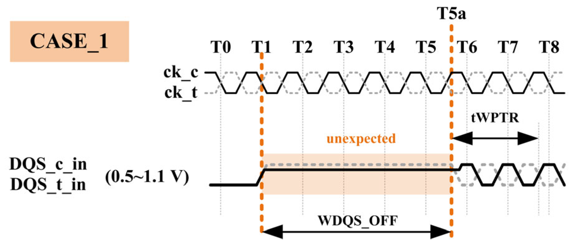
In mobile dynamic random access memory (DRAM), the crossover point of the data strobe complement (DQS_c) and data strobe true (DQS_t) signals is used to latch data on the DQ. Therefore, the memory controller chip triggers the transition of DQS_t and DQS_c two cycles period earlier, indicating that the DRAM is about to begin writing data, corresponding to the tWPRE timing parameter defined by the Joint Electron Device Engineering Council (JEDEC). According to the mobile DRAM specification [1], during the write preamble time (tWPRE) phase and under the write data strobe off (WDQS_OFF) mode, the DQS_t signal should maintain a voltage level below 0.3 V, referred to as a low-level voltage signal, between time periods T1 and T5a. The DQS_c signal must remain above 0.9 V, referred to as a high-level voltage signal, as shown in Figure 1.
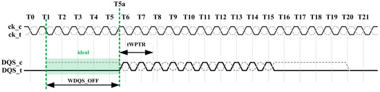
Figure 1.
The timing of the DQS signal in DRAM during the write operation [1].
Regarding the investigation of DQS signals in DRAM as a receiver, Park and Huddar [2] mentioned that intersymbol interference (ISI) is generated, distorting the DRAM signal at the receiving end when differential signals are transmitted from the DRAM controller through the channel to DRAM. They analyzed the impact of noise interference on DQS signals using the time interval error (TIE) method. Choi et al. [3] proposed a gain-enhanced active-inductive continuous-time linear equalizer (GE-AI CTLE) circuit architecture to enhance low-frequency gain and improve the DRAM receiver’s ability to cope with ISI. Zhang et al. [4] mentioned that glitches caused by high-impedance (high-z) noise severely affect the signal integrity received at the DQS port. To correct unexpected voltage levels, Jeong et al. [5] provided a current mirror-based voltage regulation circuit with logic error detection, which can adjust erroneous voltage levels and output larger voltage swings. In 2023, Balaji et al. [6] proposed a voltage regulation circuit architecture that uses fewer metal-oxide-semiconductor field-effect transistors (MOSFETs) to raise the input voltage from below to above the threshold, with a single-ended differential voltage output.
2. System Architecture
The system architecture developed in this study is shown in Figure 2. The system consists of three modules: test patterns, voltage regulation, and the approximately ideal level. In the test pattern module, three cases of unexpected signals are predefined as test inputs. The voltage regulation module receives the unexpected signals at the front end, adjusts the signal levels, and outputs the modified signals at the back end. The approximately ideal level module receives the adjusted signals and transmits them to the DQS_t and DQS_c ports of the mobile DRAM.
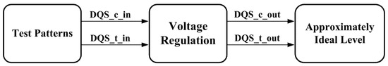
Figure 2.
System architecture and validation process.
2.1. Test Patterns
In the mobile DRAM, when DQS_c and DQS_t function as receivers, the voltage levels of the transmitted signals often deviate from the spec-defined levels due to the inherent characteristics of the transmission or the effects of temperature variations and intersymbol interference (ISI) during the transmission process. These deviations are considered unexpected signal levels. We classified these unexpected signal levels into three cases. Therefore, we used Cadence HSPICE software to simulate these three cases of unexpected voltage levels as input test conditions.
CASE_1 describes an unexpected test signal, where the voltage swing of DQS_c_in and DQS_t_in remains between 0.5 and 1.1 V during the timing period from T1 to T5a, as shown in Figure 3. This Case 1 signal serves as one of the input test conditions for the voltage regulation circuit.
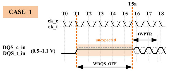
Figure 3.
Diagram of testing unexpected input signals at high-state levels.
CASE_2 represents the DQS_c_in and DQS_t_in signals exhibiting a mid-level voltage fluctuation between 0.5 V and 0.65 V during the timing period from T1 to T5a, as shown in Figure 4.
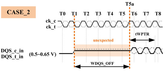
Figure 4.
Diagram of testing unexpected input signals at mid-state levels.
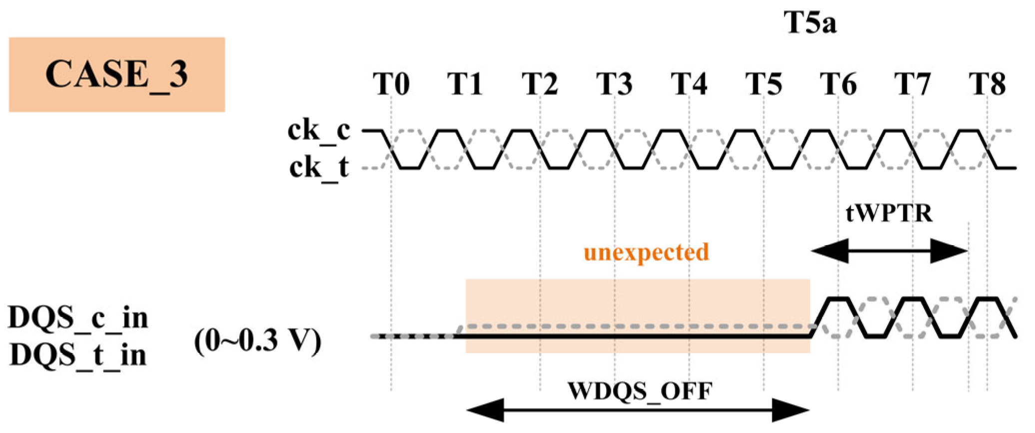
CASE_3 involves the DQS_c_in and DQS_t_in signals with a low voltage swing between 0 V and 0.3 V during the timing period from T1 to T5a, as shown in Figure 5.
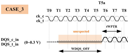
Figure 5.
Diagram of testing unexpected input signals at low-state levels.
2.2. Voltage Regulation
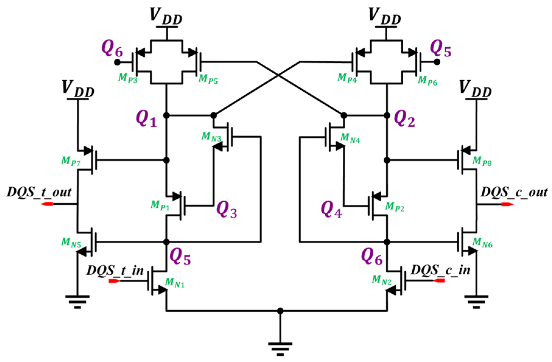
The voltage regulation proposed by Balaji et al. [6] only has a single-ended output. We modified their circuit by adding an inverter (composed of and ) between the source terminal () and the drain terminal () of the P-Type MOSFET, and then we set the voltage parameter to 1.1 V, as specified in the DRAM specification [1], as shown in Figure 6.
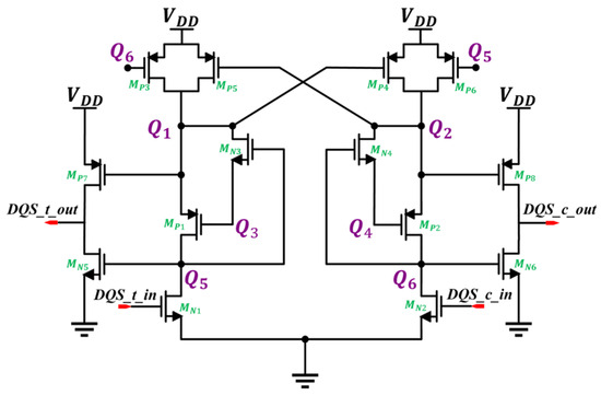
Figure 6.
Modifications of provided voltage regulation circuit.
2.3. Approximately Ideal Level
In this study, Cadence HSPICE was used to generate three cases of unexpected voltage signals as input test patterns for the voltage regulation circuit. The voltage regulation circuit adjusts these input patterns (i.e., the three cases of unexpected voltage signals) to produce output voltages that are close to the ideal levels. The low voltage of DQS_t_out is lower than or equal to 0.3 V, while the high voltage of DQS_c_out is higher than or equal to 0.9 V, as shown in Figure 7. These outputs comply with the specification requirements [1].
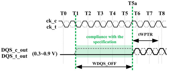
Figure 7.
Specification-compliant level obtained after voltage level regulation.
3. Results
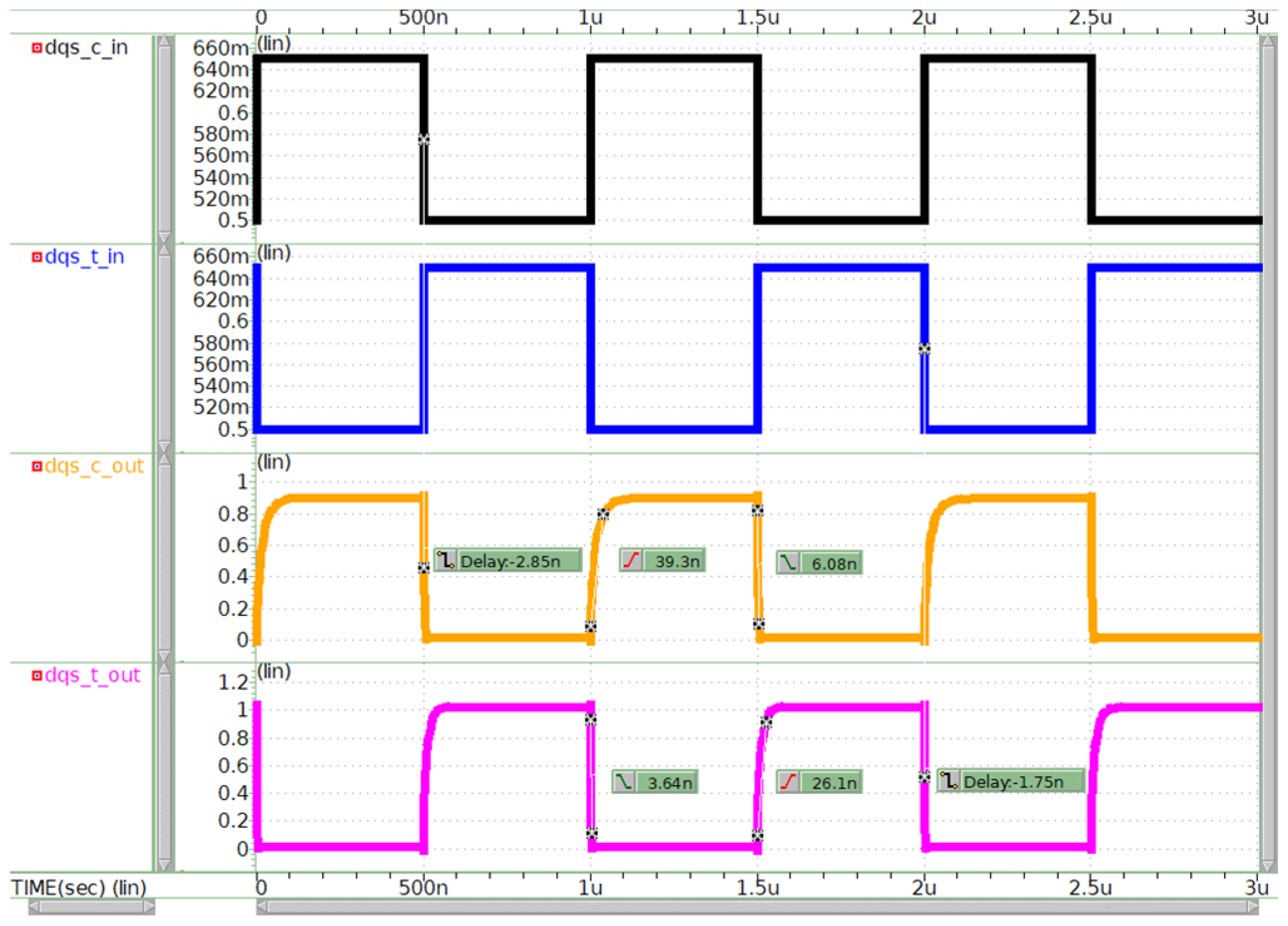
In the simulation experiment using Cadence HSPICE software, we set the test pattern for Case 1 such that DQS_c_in and DQS_t_in remain within the high-state swing range of 0.5 to 1.1 V, as shown in the first and second rows of Figure 8, and these signals were used as inputs to the voltage regulation circuit. The final output signals from the voltage regulation circuit were DQS_c_out, which met the specification with a high-state level above 0.9 V from 0 to 500 ns, and DQS_t_out, which met the specification with a low-state level below 0.3 V from 0 to 500 ns, as shown in the third and fourth rows of Figure 8. The output signals, DQS_c_out and DQS_t_out, were then connected to the DQS ports of the mobile DRAM.
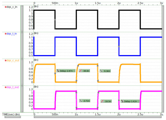
Figure 8.
Simulation of CASE_1 before and after voltage level regulation.
The test pattern for Case 2 sets DQS_c_in and DQS_t_in within the swing range of 0.5 to 0.65 V, as shown in the first and second rows of Figure 9. These signals are used as inputs to the voltage regulation circuit. The output signals from the voltage regulation circuit are DQS_c_out and DQS_t_out, as shown in the third and fourth rows of Figure 9.

Figure 9.
Simulation of CASE_2 before and after voltage level regulation.
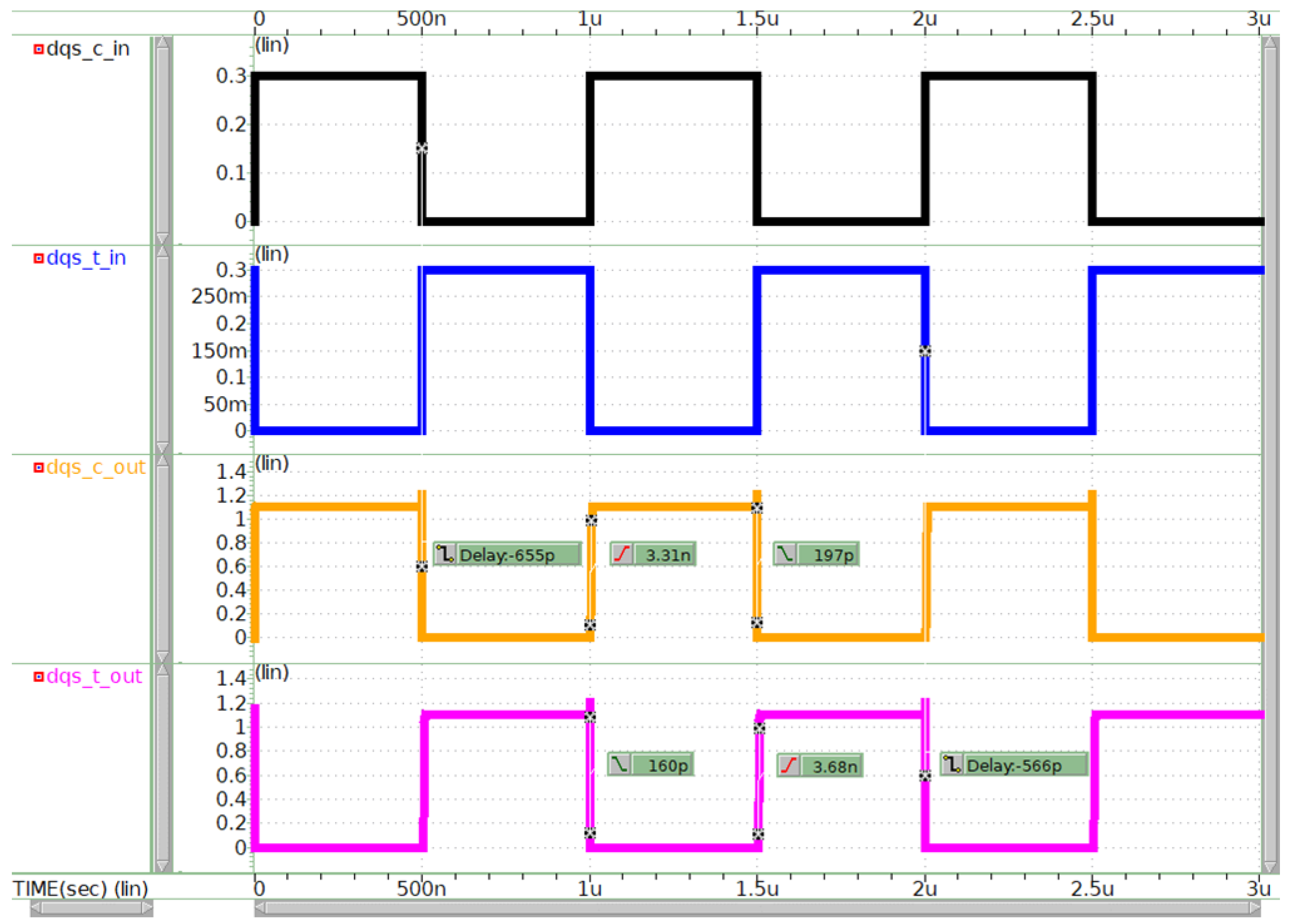
The test pattern for Case 3 sets DQS_c_in and DQS_t_in within the low-state swing range of 0 to 0.3 V, as shown in the first and second rows of Figure 10, and these signals are used as inputs to the voltage regulation circuit. The output signals from the voltage regulation circuit are DQS_c_out and DQS_t_out, as shown in the third and fourth rows of Figure 10.
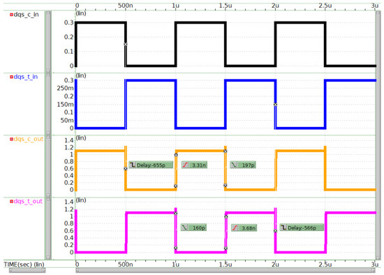
Figure 10.
Simulation of CASE_3 before and after voltage level regulation.
The wave crest of the output signal, DQS_c_out, remains above 0.9 V, while the trough voltage of DQS_t_out is maintained below 300 mV. The average delay time for DQS_c_out is 2.12 ns, and for DQS_t_out, it is 1.24 ns. The average rise and fall times for DQS_c_out are 27.1 ns and 4.205 ns, respectively. Similarly, the average rise and fall times for DQS_t_out are 15.42 ns and 2.17 ns, as shown in Table 1.

Table 1.
Characteristic parameters of output voltage signals from simulation results.
4. Conclusions
We developed a differential signal pair voltage regulation circuit for the DQS_t and DQS_c ports on the DRAM receiver side. The circuit was capable of adjusting unexpected input signal voltages, ensuring that the output signal DQS_c_out was above 0.9 V and DQS_t_out was below 0.3 V. We employed 90 nm MOSFET technology, and experimental results demonstrated that the average delay time for DQS_c_out was 2.12 ns and that for DQS_t_out was 1.24 ns at a frequency of 1 MHz. The delay time for DQS_t was 9.76 ns shorter than that achieved using the 65 nm MOSFET technology developed by Balaji et al. [6] and 16.44 ns shorter than that achieved using the 55 nm MOSFET technology developed by You et al. [7], as shown in Table 2.
Table 2.
Comparison of signal transmission delay times between voltage regulation circuit architectures for Balaji et al. [6] and You et al. [7].
Author Contributions
Conceptualization, Y.-Z.Z. and C.-A.C.; methodology, Y.-Z.Z.; software, V.-K.N.; validation, B.-Y.L.; resources, P.H.; writing—original draft preparation, Y.-Z.Z.; writing—review and editing, C.-A.C., P.H., V.-K.N. and B.-Y.L. All authors have read and agreed to the published version of the manuscript.
Funding
This work was supported, in part, by the National Science and Technology Council (NSTC), Taiwan, under grant number 113-2221-E-131-026.
Institutional Review Board Statement
Not applicable.
Informed Consent Statement
Not applicable.
Data Availability Statement
Data are available in this manuscript.
Conflicts of Interest
The authors declare no conflicts of interest.
References
- Low Power DRAM, LPDDR4 SDRAM. 2024. Available online: https://www.nanya.com/tw/Product/4291/NT6AN1024F32AV-J2 (accessed on 29 April 2025).
- Park, S.; Huddar, V.A. Time Interval Error (TIE)-based SI Design and Characterization of DDR5 Data Strobe Signaling. In Proceedings of the 2023 IEEE 25th Electronics Packaging Technology Conference (EPTC), Singapore, 5–8 December 2023; pp. 303–306. [Google Scholar] [CrossRef]
- Choi, J.; Choi, Y.; Sim, J.; Kwon, Y.; Park, S.; Kim, S.; Sim, C.; Kim, C. A Single-Ended NRZ Receiver with Gain-Enhanced Active-Inductive CTLE and Reference-Selection DFE for Memory Interfaces. IEEE J. Solid-State Circuits 2024, 59, 1261–1270. [Google Scholar] [CrossRef]
- Zhang, X.; Lee, B.; Eom, C.; Pang, G.; Jung, J. Pseudo differential DQS receiver for eliminating channel Hi-z noise. In Proceedings of the 2023 IEEE 15th International Conference on ASIC (ASICON), Nanjing, China, 24–27 October 2023; pp. 1–3. [Google Scholar] [CrossRef]
- Jeong, H.; Kim, T.-H.; Park, C.N.; Kim, H.; Song, T.; Jung, S.-O. A Wide-Range Static Current-Free Current Mirror-Based LS with Logic Error Detection for Near-Threshold Operation. IEEE J. Solid-State Circuits 2021, 56, 554–565. [Google Scholar] [CrossRef]
- Balaji, R.; Siddharth, R.K.; Naik, S.; Kumar, Y.B.N.; Vasantha, M.H.; Bonizzoni, E. A 11-ns, 3.85-fJ, Deep Sub-threshold, Energy Efficient Level Shifter in 65-nm CMOS. In Proceedings of the 2023 IEEE International Symposium on Circuits and Systems (ISCAS), Monterey, CA, USA, 21–25 May 2023; pp. 1–5. [Google Scholar] [CrossRef]
- You, H.; Yuan, J.; Tang, W.; Qiao, S.; Hei, Y. An Energy-Efficient Level Shifter for Ultra Low-Voltage Digital LSIs. IEEE Trans. Circuits Syst. II Express Briefs 2020, 67, 3357–3361. [Google Scholar] [CrossRef]


Disclaimer/Publisher’s Note: The statements, opinions and data contained in all publications are solely those of the individual author(s) and contributor(s) and not of MDPI and/or the editor(s). MDPI and/or the editor(s) disclaim responsibility for any injury to people or property resulting from any ideas, methods, instructions or products referred to in the content. |
© 2025 by the authors. Licensee MDPI, Basel, Switzerland. This article is an open access article distributed under the terms and conditions of the Creative Commons Attribution (CC BY) license (https://creativecommons.org/licenses/by/4.0/).