Abstract
Quantum-dot cellular automata (QCA) offer a high-performance, low-power alternative to traditional VLSI technology for nanocomputing. However, the existing metal-dot QCA-based parity generators and checker circuits suffer from increased energy dissipation, larger area consumption, and complex multilayered layouts, limiting their practical feasibility. This work designs a 3-bit parity generator and 4-bit checker to address these challenges using an optimized modified majority voter-based Ex-OR gate in QCA. A single-layered layout was simulated in QCADesigner 2.0.3, avoiding crossovers to reduce fabrication complexity. Energy analysis using QCADesigner-E reveals 34.4 meV energy consumption, achieving 31% energy efficiency and 75% area efficiency in the context of QCA costs compared to recent designs. The proposed circuit highlights the unique potential of QCA as a scalable, energy-efficient solution for high-density next-generation computing systems.
1. Introduction
The search for alternatives to the scaling and shrinking issues of CMOS devices has intensified, as traditional transistor-based technology faces challenges such as increased leakage currents, higher power dissipation, and quantum effects at nanoscales [1,2]. The silicon-based semiconductor quantum-dot cellular automata (QCA) present a promising paradigm shift, leveraging the position of electrons within quantum dots to perform logic operations (binary states ‘0’ and ‘1’) in a quantum-equation-based computational model [3,4,5]. QCA operates using the Coulombic interaction between electrons in a cell of four quantum dots, typically with a cell size of 18 nm × 18 nm [4,5]. Binary states are represented with stable arrangements of electrons [3,5], as illustrated in Figure 1a. These binary states are generated through specific electron arrangements, in which two mobile electrons [5] occupy opposite diagonal positions to minimize repulsion [3,4]. A few basic blocks, such as QCA wires [6], inverters [7], and majority gates, help design any circuit in QCA. QCA wires enable signal transmission by facilitating polarization propagation between adjacent cells, ensuring data integrity. Figure 1b depicts the Landauer clocking of QCA cells, which is necessary for information propagation through a sinusoidal E-field [8] and controls circuit operation through four sequential phases: relax, switch, hold, and release [3,8]. This ensures a synchronized data flow through the wire in Figure 1c and prevents race conditions to reduce the latency of nano-circuits. The parity generator and checker circuits in QCA nanoprocessors ensure reliable data transmission and error detection using Ex-OR gates.
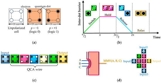
Figure 1.
Basic figures of the QCA paradigm: (a) quantum-dot cells; (b) cell clock phases; (c) wire; (d) MMV gate layout.
Motivated by the need for highly efficient and reliable error detection circuits in QCA-based computing, this work aims to enhance the performance of parity generator and checker circuits. While prior studies have explored conventional majority voter-based parity circuits, they often suffer from increased latency and area constraints. This work introduces a QCA parity generator and checker using a modified majority voter (MMV) [9,10], as per Figure 1d, that enhances efficiency and performance. This logic gate achieves significant reductions in energy consumption and area cost by reducing cell counts through implementing asymmetric cell placement and shared cell boundaries while maintaining logic functionality, and it minimizes clock zones by aligning the output cell with downstream logic, eliminating buffer zones, and reducing both energy and latency by one clock cycle and thereby reducing state-switching energy requirements [10].
The key contributions of this work include the following:
- (I)
- A novel QCA-based parity generator and checker circuit leveraging an optimized MMV design.
- (II)
- Improved efficiency in terms of area, delay, and energy dissipation compared to conventional designs.
- (III)
- A comparative analysis demonstrating the advantages of the proposed approach over existing state-of-the-art QCA parity circuits.
2. Related Works
Parity generator/checker circuits are essential building blocks in fault-tolerant systems. Therefore, many existing parity generator/checker layouts in QCA highlight their advantages and disadvantages. A few of these are discussed here.
Naz et al. introduced a 4-bit even parity checker [11] based on a fault-tolerant XOR gate. This checker, leveraging 414 cells, does not involve any parity generator circuit; the user gives input bits as arbitrary parity bits to be able to perform parity checks after 4 clock-delay. This work assessed energy details for the XOR design but overlooked the checker unit, which uses excessive logic gates to produce an output. The design in [12] uses 118 cells, covering 0.17 μm2, with a delay of 1.25 clock cycles. Despite quantified energy dissipation and the use of crossovers, the design remains complex and lacks compactness when employing crossovers. In [13], V. K. Sharma suggested a highly compact and efficient design using only 18 cells with a minimal area of 0.01 μm2 and a delay of 0.50 clock cycles. The simplicity is attributed to a single parity generator, excluding a checker unit. The design in [14] uses 98 cells, covering 0.09 μm2, with a delay of 1.50 clock cycles. Though moderately efficient, its higher energy dissipation makes it suitable for specific applications. In [15], the circuit integrates 62 cells in a 0.08 μm2 area, achieving a delay of 2.00 clock cycles. While it uses the highest logic gates, it suffers from performance due to energy inefficiencies. The circuit in [16] uses 55 cells, covers 0.09 μm2, and involves a delay of 1.50 clock cycles with energy dissipation of ~16 meV. It shows moderate efficiency, balancing performance and resource utilization. The design in [17] balances size and performance, using 86 cells and covering 0.10 μm2 with a delay of 1.50 clock cycles. However, energy dissipation data are missing, making it difficult to assess the circuit’s efficiency in nanocomputing. Based on the above discussion, earlier designs focus on robustness but suffer from issues related to energy dissipation and costs.
The proposed design balances area, energy efficiency, and scalability, overcoming the limitations of earlier works and setting a cost-effective benchmark for future research. Here are the key novelty points of your work beyond just cascading XOR gates for designing the parity block:
- Instead of conventional XOR cascades, the work employs a modified majority-voter (MMV)-based XOR gate, improving logic efficiency and reducing latency.
- The proposed design avoids multilayered crossovers, simplifies fabrication, and enhances layout feasibility and thermal stability for practical implementation.
- Compared to recent designs, the circuit achieves better energy efficiency, as validated using a specific tool.
- The design also achieves area efficiency, making it suitable for high-density computing applications.
- The optimized structure ensures a minimal delay overhead, improving the real-time reliability of QCA-based parity circuits. The methodology can be extended to design higher-bit parity generators and checkers while maintaining efficiency advantages.
3. Methods
A 3-bit even parity generator outputs a parity bit, PG_out, of 1 when the number of high inputs is odd, and 0 otherwise. The logic of the even parity generator can be logically expressed as follows:
where A, B, and C are the input bits. Table 1 illustrates the corresponding logic table for the generator. For error detection, a parity checker verifies the parity of the received 4-bit message, consisting of three data bits and the parity bit PG_in. The receiver expects an even number of 1s in the message. Figure 2a represents the design schematic of the entire unit to illustrate the design strategy in the context of QCA nanocomputing, aiming to achieve novelty. If a discrepancy is found, the parity checker signals an error. The checker’s logic is expressed as follows:

Table 1.
Even parity generator logic table.
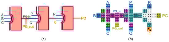
Figure 2.
Proposed circuit: (a) schematic; (b) layout.
Here, P, Q, R, and PG_in represent the inputs, with the logic table detailed in Table 2. The proposed QCA layout, as depicted in Figure 2b, which functions as an even parity generator and a parity checker, uses an efficient MMV-based Ex-OR gate for each circuit. The MMV-based Ex-OR gate enhances reliability and energy efficiency in parity operations. The use of this MMV in the proposed design does not restrict its applicability to specific QCA realizations, as it remains compatible with both clocking-based and energy-driven QCA models. Its compact design, by optimizing cell placement with strategic clocking, lowers switching energy and footprint. Efficient clocking ensures adiabatic operation with reduced kink energy compared to conventional majority gates. However, its technological validity depends on fabrication feasibility, robustness against defects, and scalability, which require further exploration in practical QCA implementations [10]. Using the QCADesigner 2.0.3 [18] tool, the proposed layout implements the parity generator and checker circuits with just three MMVs, achieving a 1.00 clock cycle delay. For the generator, an MMV-based TIEO (three-input exclusive OR) gate [10] processes inputs A, B, and C to produce PG_out. For the checker, two TIEO gates and one 2-input MMV-based Ex-OR gate handle inputs P, Q, R, and PG_in, and their outputs are combined to determine the final checker output PC without employing any crossover. It is a single-layer QCA layout consisting of 37 cells, requiring a total area of 0.05 µm2, with each cell occupying 0.011 µm2. This compact and efficient design demonstrates the potential of QCA technology for reliable, low-power data communication systems.
Table 2.
Even parity checker logic table.
4. Results and Discussions
In the context of the proposed QCA parity generator/checker layout for the parity checker, the inputs P, Q, and R are used to verify the functionality of the parity-checking circuit along with the generated parity bit, PG_in. The specific cases of P = 1, Q = 0, and R = 0 are considered during simulation to test how the circuit responds to different input combinations and ensure that it correctly computes the parity based on these inputs. The parity checker is expected to determine the parity of the inputs and produce the correct output, PC, following Equations (1) and (2), as shown in Figure 3a. Another expected output is represented in Figure 3b, setting input combinations according to Table 2. These thorough tests are crucial to confirm the reliability and correctness of the circuit design.
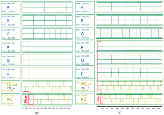
Figure 3.
Simulation outputs of proposed circuit: (a) that considering P = 1, Q = 0, and R = 0; (b) that considering input values indicated in Table 2.
In QCA circuits, the average output polarization (AOP) serves as a critical metric for evaluating signal integrity, calculated as the arithmetic mean of the maximum (+Pmax) and minimum (−Pmin) output polarization values [19] expressed in Equation (3).
A high AOP (≥0.85) value indicates robust binary state representation, where +1.00 and −1.00 correspond to perfect logic ‘1’ and ‘0’ states, respectively. For the proposed design, QCA simulations (Figure 3) demonstrate an AOP of 0.953 for both outputs, simulating at a temperature range of 1 K to 4 K and confirming strong noise immunity. This outperforms the suggested layout, which involves optimized cell geometry and clock synchronization, which minimize polarization decay. The AOP metric is particularly vital for assessing thermal resilience, as it quantifies signal degradation under thermal fluctuations.
Energy dissipation analysis in QCA nanocomputing is crucial for evaluating circuit energy efficiency. The proposed circuit dissipates a total energy (TE) of 34.4 meV, simulated by the coherence vector simulation engine at a default clock frequency (TC) of 0.25 THz per clock for adiabatic switching [20], with an average energy dissipation of 3.13 meV per cycle using the QCADesigner-E 2.2 [20] tool. This implies that the real-time circuit latency indicates the same in clock cycles divided by the simulation clock frequency calculated for the conventional Landauer clocking scheme of the QCA-based clock distribution network [8].
Costs in QCA are also key metrics for evaluating circuit efficiency [4]. The area-delay cost (AD cost) measures the trade-off between circuit size and speed, calculated as 0.05 units for the proposed circuit. The energy-delay cost (ED cost) assesses energy efficiency relative to operational speed, valued at 0.00033 units. The QCA-specific cost (QCA cost) combines design factors like logic gates count, crossovers and layer counts, and delay, which is 9 units for this design, calculated using Equations (4)–(6).
Here, the total area, energy, and delay are measured in μm2, eV, and clock cycles, whereas l and QC indicate the number of layers and crossovers.
The introduced circuit was carefully designed to ensure both scalability and thermal stability within the operational constraints of single-layer non-molecular QCA architectures. The modular design approach allows for straightforward extension to higher bit-widths. All input/output nodes are strategically positioned at the periphery of the circuit layout for clean signal access while avoiding the routing congestion that typically complicates single-layer designs. Regarding thermal stability, while this methodology acknowledges the inherent cryogenic requirements of non-molecular QCA systems, this design incorporates robust clocking zones and optimized cell placement to maximize polarization retention, with the simulation results indicating reliable operation up to 4K when compared against experimental data from prior QCA realizations. The circuit’s thermal resilience is further enhanced by its minimized cross-wiring and balanced cell loading, which collectively reduce susceptibility to thermal noise. These architectural decisions address current scalability challenges and provide a foundation for potential integration with emerging room-temperature QCA technologies as material advancements progress.
5. Comparisons
The proposed scalable parity generator and checker circuit requires at least 18 fewer cells than the designs reported in Table 3, offering a 0.25 clock cycle reduction in delay compared to the best design in [12]. In terms of cost efficiency, the circuit is 31% more energy-delay cost-effective than [14] and 75% more area-delay cost-effective than the design in [16] due to its faster operational speed and optimized layout. Additionally, the proposed circuit demonstrates a 94% improvement in QCA-specific cost compared to the design in [12]. The designs in [11,13] are not directly comparable, as they do not have a parity generator and checker circuits, respectively.
Table 3.
Design parameters comparison table.
6. Conclusions
The proposed QCA-based parity generator and checker offers a dual-functional, energy-efficient design for error detection in communication systems. Using an optimized MMV-based Ex-OR gate, the circuit achieves compactness, reduced energy dissipation, and enhanced reliability, making it suitable for low-power, high-performance, scalable nanocomputing. It shows 31% energy efficiency and 75% area efficiency compared to the latest QCA-based circuits. This single-layer crossover-free design eliminates complex multilayer interconnects and reduces fabrication challenges in both non-molecular and molecular QCA systems by simplifying layout alignment and minimizing signal interference during integration. Future work will focus on implementing this design in nano-circuits for real-world applications, and its methodology could be extended to advanced error-correcting mechanisms in the molecular QCA framework and other digital circuits in next-generation technologies.
Author Contributions
Conceptualization, R.K.S. and A.K.; methodology, R.K.S.; software, R.K.S. and A.K.; validation, R.K.S. and A.K.; formal analysis, R.K.S. and A.K.; investigation, R.K.S. and A.K.; resources, R.K.S. and A.K.; writing—original draft preparation, R.K.S.; writing—review and editing, A.K.; visualization, R.K.S.; supervision, A.K.; project administration, A.K. All authors have read and agreed to the published version of the manuscript.
Funding
This research received no external funding.
Institutional Review Board Statement
Not applicable.
Informed Consent Statement
Not applicable.
Data Availability Statement
All data generated or analyzed during this study are included in this article.
Conflicts of Interest
The authors declare no conflicts of interest.
References
- Safoev, N.; Jeon, J.-C. Design and evaluation of cell interaction based vedic multiplier using quantum-dot cellular automata. Electronics 2020, 9, 1036. [Google Scholar] [CrossRef]
- Walus, K.; Schulhof, G.; Jullien, G.A.; Dimitrov, V.S. High level exploration of quantum-dot cellular automata. In Proceedings of the Conference Record of the Thirty-Eighth Asilomar Conference on Signals, Systems and Computers, Pacific Grove, CA, USA, 7–10 November 2004; pp. 30–33. [Google Scholar] [CrossRef]
- Lent, C.S.; Tougaw, P.D.; Porod, W.; Bernstein, G.H. Quantum cellular automata. Nanotechnology 1993, 4, 49–57. [Google Scholar] [CrossRef]
- Ahmed, T.; Younes, A.; Elkabani, I. Multi-strategy based quantum cost reduction of quantum boolean circuits. Phys. Scr. 2024, 100, 015102. [Google Scholar] [CrossRef]
- Vankamamidi, V.; Ottavi, M.; Lombardi, F. A serial memory by quantum-dot cellular automata (QCA). IEEE Trans. Comput. 2008, 57, 606–618. [Google Scholar] [CrossRef]
- Pramanik, A.K.; Pal, J.; Sen, B. Analysis of fault tolerance capability of QCA circuit under regular clocking. Int. J. Electron. 2025, 1–23. [Google Scholar] [CrossRef]
- Tougaw, P.D.; Lent, C.S. Logical devices implemented using quantum cellular automata. J. Appl. Phys. 1994, 75, 1818–1825. [Google Scholar] [CrossRef]
- Ottavi, M.; Pontarelli, S.; DeBenedictis, E.; Salsano, A.; Kogge, P.; Lombardi, F. High throughput and low power dissipation in QCA pipelines using Bennett clocking. In Proceedings of the IEEE/ACM International Symposium on Nanoscale Architectures, Anaheim, CA, USA, 17–18 June 2010; pp. 17–22. [Google Scholar] [CrossRef]
- Navi, K.; Farazkish, R.; Sayedsalehi, S.; Azghadi, M.R. A new quantum-dot cellular automata full-adder. Microelectron. J. 2010, 41, 820–826. [Google Scholar] [CrossRef]
- Bahar, A.N.; Ahmad, F.; Wani, S.; Al-Nisa, S.; Bhat, G.M. New modified-majority voter-based efficient QCA digital logic design. Int. J. Electron. 2018, 106, 333–348. [Google Scholar] [CrossRef]
- Naz, S.F.; Shah, A.P.; Ahmed, S. QCA-based fault-tolerant XOR gate for reliable computing with high thermal stability. Phys. Scr. 2024, 99, 065120. [Google Scholar] [CrossRef]
- Khan, A.; Bahar, A.N.; Arya, R. Quad-functioning parity layout for nanocomputing: A QCA design. Nano Commun. Netw. 2024, 41, 100525. [Google Scholar] [CrossRef]
- Sharma, V.K. Parity generators in QCA nanotechnology for nanocommunication systems. Nano Commun. Netw. 2023, 36, 100440. [Google Scholar] [CrossRef]
- Tapna, S.; Chakrabarti, K.; Mukhopadhyay, D. A secure communication gateway with parity generator implementation in QCA platform. In Computational Intelligence in Communications and Business Analytics; Mukhopadhyay, S., Sarkar, S., Dutta, P., Mandal, J.K., Roy, S., Eds.; Communications in Computer and Information Science; Springer: Berlin/Heidelberg, Germany, 2022; Volume 1579, pp. 197–209. [Google Scholar] [CrossRef]
- Raman, S.; Samanvita, N.; Ahmed, T.; Aishwarya, A.; Karthiganesh, D. Implementation of parity generator and checker using quantum-dot cellular automata. In Proceedings of the IEEE 2nd Mysore Sub Section International Conference (MysuruCon), Mysuru, India, 16–17 October 2022; pp. 1–8. [Google Scholar] [CrossRef]
- Fazili, M.M.; Jahangir, R.; Tripathi, N. Novel parity generator and detector design using quantum dots. In Proceedings of the 6th International Conference for Convergence in Technology (I2CT), Maharastra, India, 2–4 April 2021; pp. 1–6. [Google Scholar] [CrossRef]
- Khakpour, M.; Gholami, M.; Naghizadeh, S. Parity generator and digital code converter in QCA nanotechnology. Int. Nano Lett. 2020, 10, 49–59. [Google Scholar] [CrossRef]
- Walus, K.; Dysart, T.J.; Jullien, G.J.; Budiman, R. QCADesigner: A rapid design and simulation tool for quantum-dot cellular automata. IEEE Trans. Nanotechnol. 2004, 3, 26–31. [Google Scholar] [CrossRef]
- Shaw, R.K.; Khan, A. Implementation of adders using XOR gates in quantum-dot cellular automata with physical verification. Phys. Scr. 2024, 99, 125108. [Google Scholar] [CrossRef]
- Torres, F.L.; Wille, R.; Niemann, P.; Drechsler, R. An energy-aware model for the logic synthesis of quantum-dot cellular automata. IEEE Trans. Comput.-Aided Des. Integr. Circuits Syst. 2018, 37, 3031–3041. [Google Scholar] [CrossRef]
Disclaimer/Publisher’s Note: The statements, opinions and data contained in all publications are solely those of the individual author(s) and contributor(s) and not of MDPI and/or the editor(s). MDPI and/or the editor(s) disclaim responsibility for any injury to people or property resulting from any ideas, methods, instructions or products referred to in the content. |
© 2025 by the authors. Licensee MDPI, Basel, Switzerland. This article is an open access article distributed under the terms and conditions of the Creative Commons Attribution (CC BY) license (https://creativecommons.org/licenses/by/4.0/).