Skip to Content
  • Proceeding Paper
  • Open Access

24 July 2024

Analysis and Synthesis of Single-Bit Adders for Multi-Bit Adders with Sequential Transfers †

,
,
,
,
and
1
International University of Information Technology, Almaty 050013, Kazakhstan
2
School of Information Technology and Engineering, Kazakh-British Technical University, Almaty 050000, Kazakhstan
3
Kazakh National University named after Al-Farabi, Almaty 050040, Kazakhstan
4
Academy of Logistics and Transport, Almaty 050012, Kazakhstan

Abstract

This paper provides an analysis of existing single-digit binary adders from the point of view of their implementation on fans built based on metal-oxide-semiconductor field-effect transistor—MOSFETs. The synthesis of a single-digit adder with a conditional sum is carried out. The considered adders are compared in terms of speed and hardware complexity (by the number of MOSFETs). Adders perform arithmetic operations on numbers. In combination with other logical operations, adders are the core of the circuits of arithmetic logic devices that implement several different operations; they are an integral part of different processors. The most important parameters of adders are their hardware complexity and performance; therefore, many options for single-bit and multi-bit connectors with serial, parallel and combined transmissions have been developed. In the final part, a scheme of a multi-bit adder with consecutive transfers on adders with a conditional sum is given. An example of performing addition operations is given.

1. Introduction

Adders perform arithmetic addition and subtraction of numbers. Together with other logical operations, adders are the core of the circuits of arithmetic logic devices that implement a number of various operations (multiplication, division, etc.), which are an indispensable part of various processors.
Important parameters of adders are their hardware complexity and performance; therefore, many variants of single-bit and multi-bit adders with serial, parallel and combined transfers have been developed [1].
The listed adders are synthesized based on the truth table. The analytical expressions of the sum (Si) and transfer functions Ci have the form:
S i = a i ¯ b i ¯ C i 1 a i ¯ b i C i 1 ¯ a i b i ¯ C i 1 ¯ a i b i C i 1 ; C i = a i b i a i   C i 1   b i   C i 1 ,
where a i ¯ and b i ¯ are the i-th digits of the numbers A and B; C i 1 —transfer from the junior category.
The formula can be reproduced on various sets of logic elements, such as AND-NOT, OR-NOT, “exclusive OR”, etc. At the same time, the hardware’s complexity and performance may be different.

2. Materials and Methods

The analysis of single-digit adders on elements is discussed below:
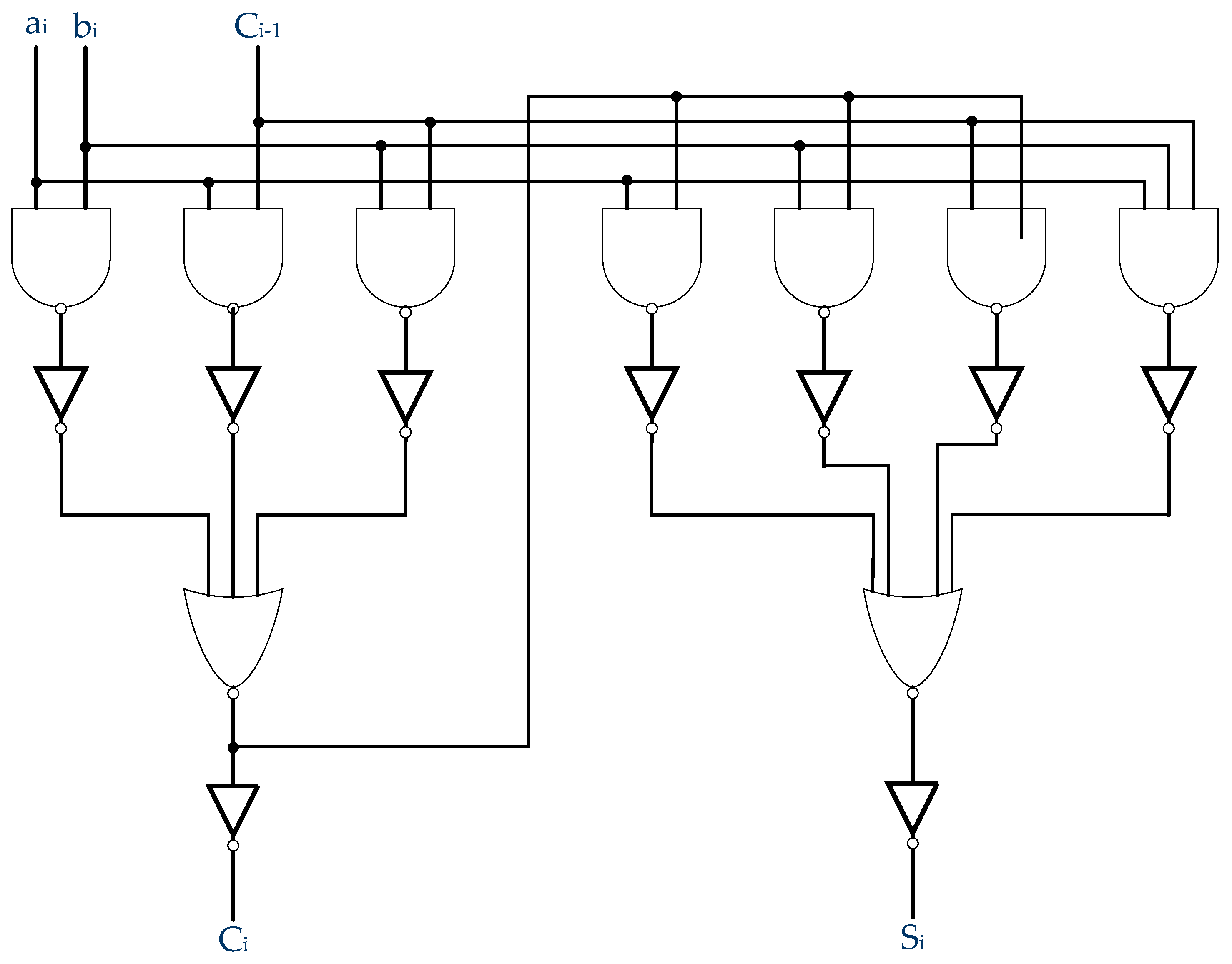
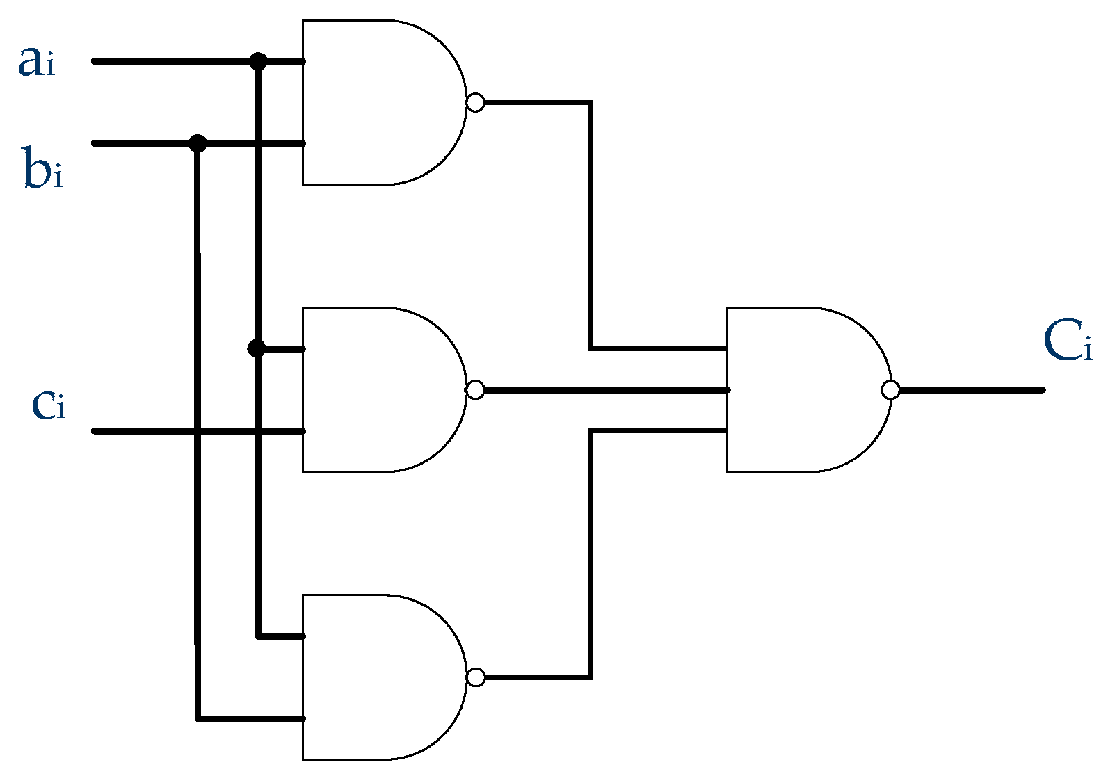
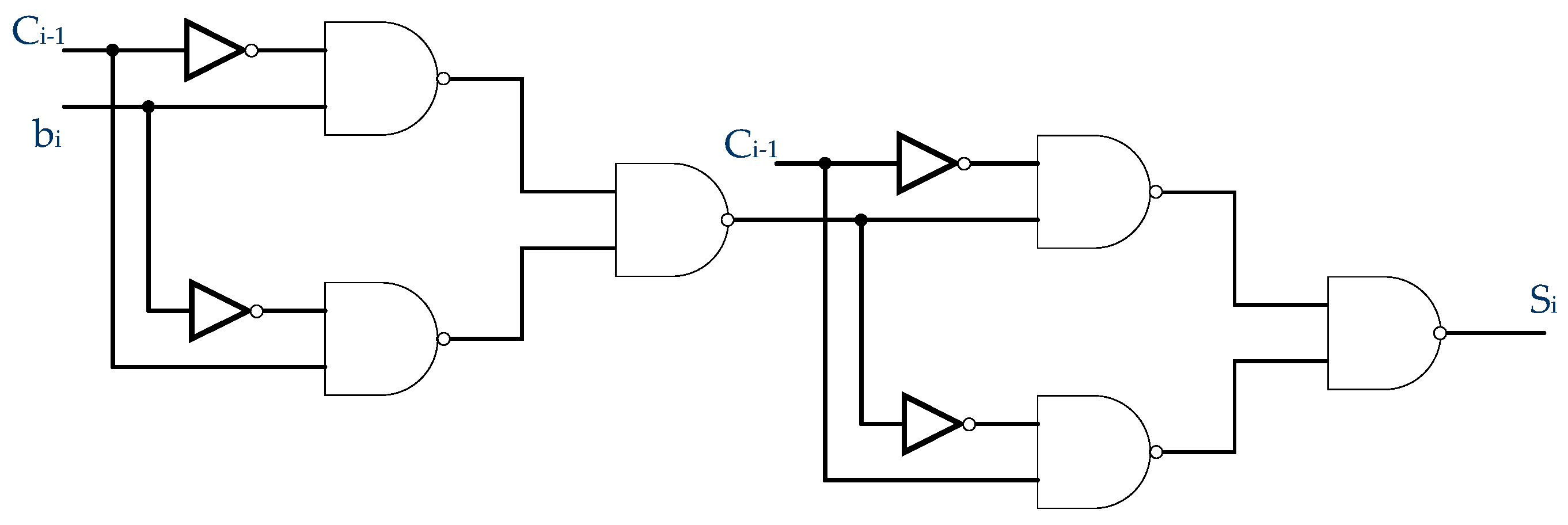
  • two-stage logic AND-OR-NOT [1];
  • two “exclusive OR” valves and OR-NOT and AND-NOT circuits [2];
  • three-way valve “exclusive OR” and circuits AND-NOT;
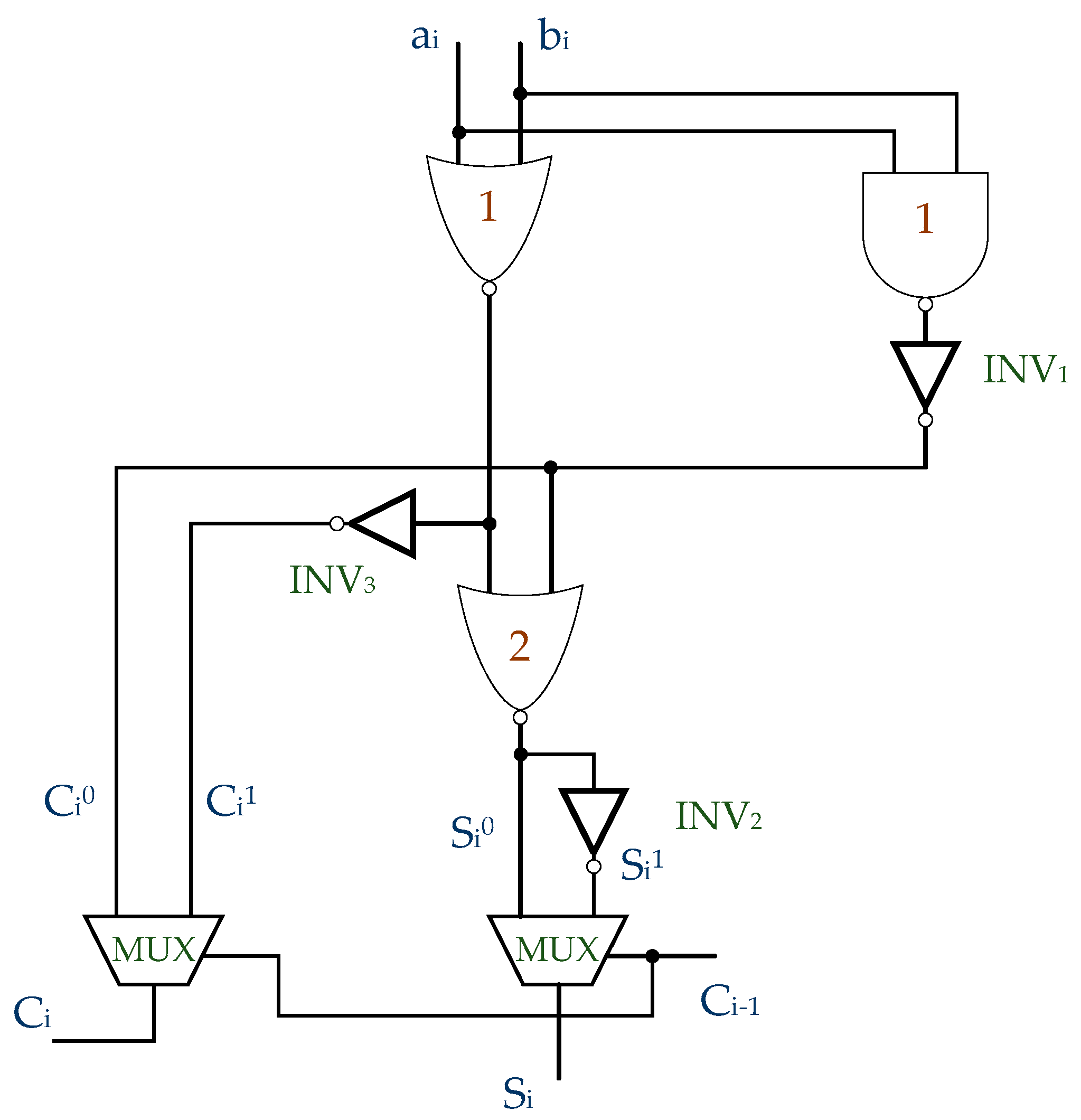
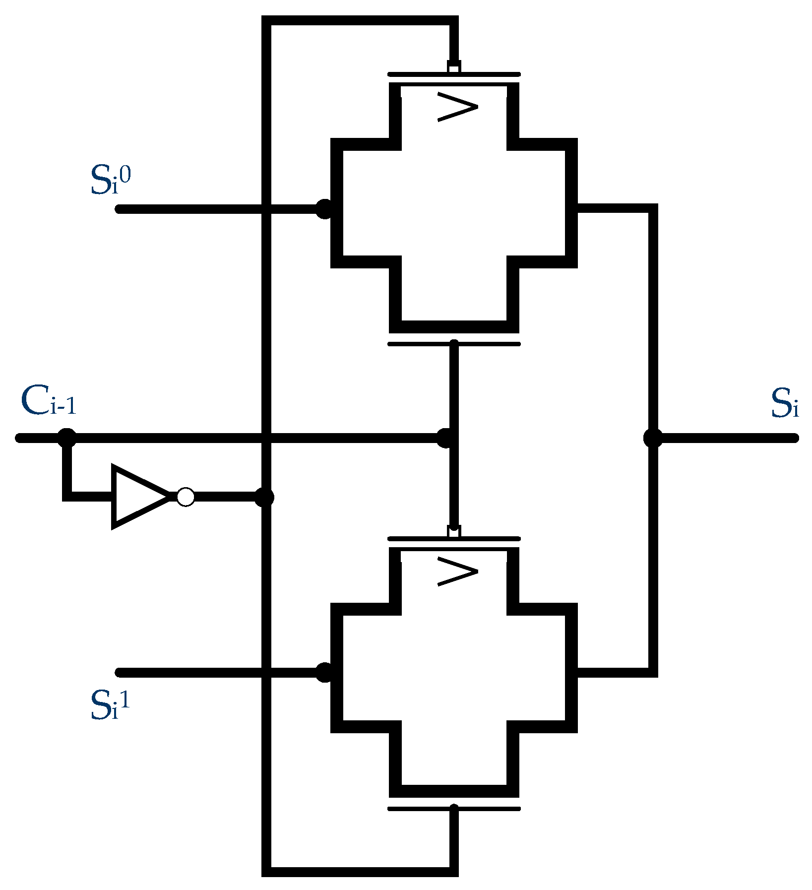
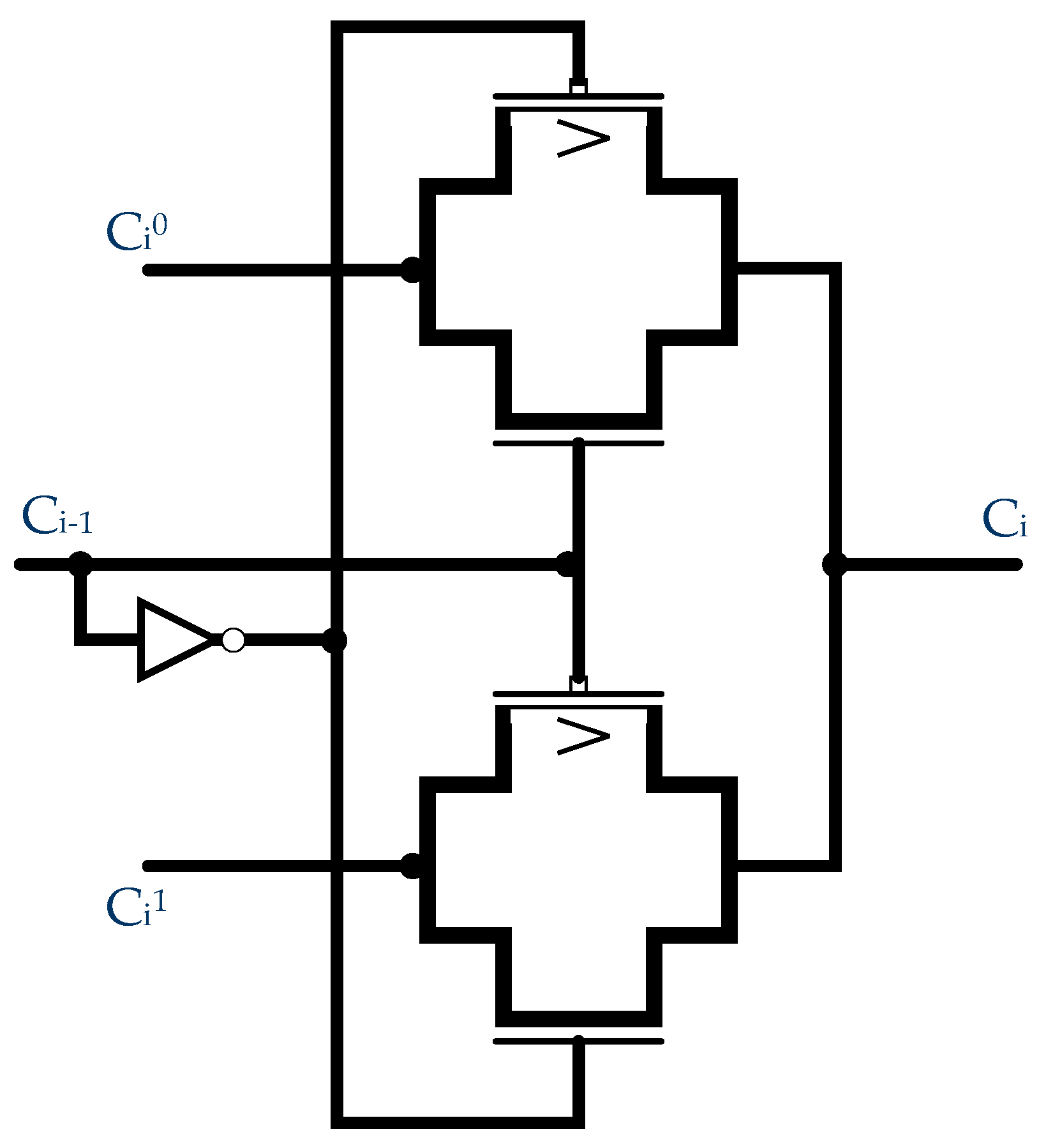
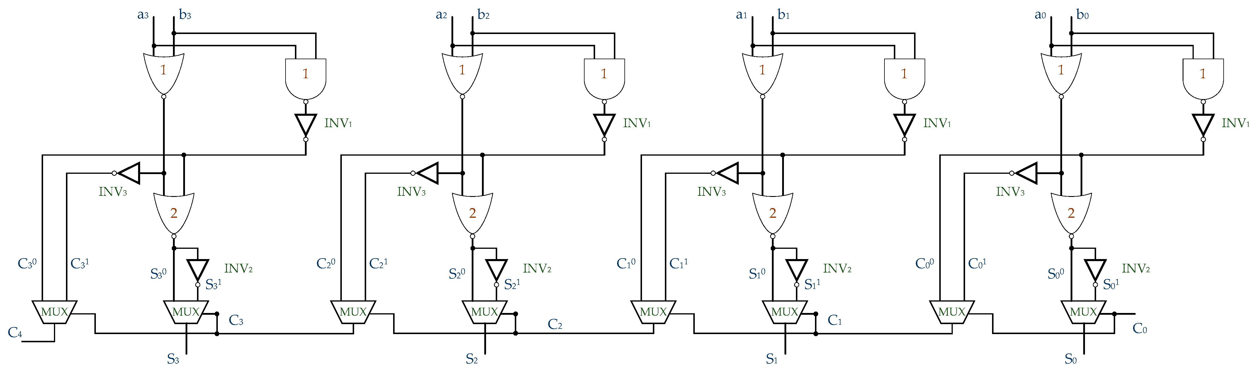
  • on valves “exclusive OR” and multiplexers, an adder with a conditional sum (conditional-sum addition_CSA) is implemented. Before determining the hardware complexity (the number of MOSFETs) and performance (the number of logic elements on which the signal is delayed), the circuits of the analyzed adders are depicted as logic gates on the MOSFET. Consider the analysis of an adder built on the basis of the two-stage logic AND-OR-NOT [1,3,4,5].
The circuit of such an adder is shown in Figure 1, and Figure 2 shows the circuit of this adder on the logic circuits of a MOSFET [6,7,8].
Figure 1. Functional diagram of the adder.
Figure 2. Logic circuit of the adder on a MOSFET.
The analytical formula of the analyzed adder has the form:
C i   = ( a i b i a i C i 1 b i C i 1 ) ; S i = C i 1 ¯ ( a i b i C i 1 ) a i b i C i 1 .
Figure 1 shows the functional diagram of the adder constructed according to Formula (2).
Figure 2 shows its logic circuit on a MOSFET.
Figure 2 shows that the adder consists of six AND-NOT circuits with two inputs each. To implement them, 6 × 4 = 24 transistors will be required. It has nine circuits of NOT (2 × 9 = 18) transistors and a gate AND-NOT for 3 inputs (6 transistors), a gate OR-NOT for 3 inputs (6 transistors) and a gate OR-NOT for 4 inputs (8 transistors). In total, 62 MOSFETs will be required to implement the adder.
The time of formation of the transfer tci = 4 τle.
The time of formation of the sum Si = 7 τle.
The second single-digit adder [2,3,9], which is subject to analysis, refers to the following formula:
S i = C i 1 a i b ; i C i = a i b i ¯   a i c i 1 ¯   b i c i 1 ¯ .
The functional scheme of the Ci transfer is shown in Figure 3, which consists of three two-input and one three-input AND-NOT circuit. To implement them, we will need (4 × 3) + 6 = 18 transistors. The time of transfer formation tci = 2 τle.
Figure 3. Functional scheme of Ci transfer.
The Si value in Formula (3) is calculated by adding modulo 2 (Si1 = ai bi), then Si = Si1  Ci−1 is calculated (the first option). Figure 4 shows a functional scheme for calculating Si based on two addition schemes modulo two.
S i 1 = a i ¯ b i a i b i ¯ ; S i =   S i 1 ¯ C i 1 S i 1 C i 1 ¯ .
Figure 4. Functional diagram of the Si calculator based on two addition schemes modulo two.
Figure 4 shows that the implementation of Si will require four inverters and six two-input AND-NOT circuits, which will require (4 × 2) + (6 × 4) = 30 transistors.
In total, to build an adder on two circuits modulo 2, we will need (18 + 32) = 50 transistors. The second adder can be built on the basis of an adder modulo two of three variables. In our case, ai, bi and Ci−1 come in as input variables. Then, the truth table for Si has the form as shown in Table 1.
Table 1. The truth table for the sum of Si.
From this table we have:
S i   = C i 1 ¯ a i ¯ b i C i 1 ¯ a i b i ¯ C i 1 a i ¯ b i ¯ C i 1 a i b i .
To calculate Si, the Formula (5) is transformed as follows:
S i   = C i 1 ¯ a ¯ b i C i 1 ¯ a i b i ¯ i C i 1 a i ¯ b i ¯ C i 1 a i b i ̿ = C i 1 ¯ a i ¯ b i ¯ ( C i 1 ¯ a i b i ¯ ) ¯ ( C i 1 a i ¯ b i ¯ ) ¯ ( C i 1 a i b i ) ¯ ¯ .
The functional scheme for the sum of Si constructed according to the Formula (6) is shown in Figure 5.
Figure 5. Functional diagram of the Si calculator based on two addition schemes modulo two.
According to Figure 5, it is not difficult to calculate that 38 MOSFETs will be required for the implementation of the Si adder.
According to Figure 3, to calculate Ci, 18 transistors will be required for a total of 56 transistors. For the formation of Si, a delay on 3 logical elements will be required, i.e., tsi = 3 τle.
Recently, the construction of so-called conditional sum adders (conditional-sum addition_ CSA) has been vigorously discussed [10,11,12,13,14].
The adder with a conditional sum is also built according to the truth table. Table 2 shows a modified table of the truth of the adder.
Table 2. Modified adder truth table.
From the first part of Table 2, where Ci−1 = 0, we have
S i 0 = a i ¯ b i a i b i ¯ ;
C i 0 = a i b i .
From the second part of Table 2, where Ci−1 = 0, we have
S i 1 = a i ¯ b i ¯ a i b i .
C i 1 = a i ¯ b i a i b i ¯ a i b i = a i b i
From this table it is also easy to see that
Si = S i 0 ¯
To construct the sum of Si0 on the fans AND-NOT, OR-NOT and NOT, Formula (7) must be reduced to the form:
S i 0 = ( a i b i ) a i b i ¯ = ( a i b i ) a i b i ¯ ¯ ¯ = a i b i ¯ + ( a i b i ) ¯ ¯ ¯
According to the Formulas (8), (10), (11) and (12) it is possible to put the functional sum of the adder on the conditional sum. At the same time, the functional circuit must be supplemented with multiplexers that are controlled by transferring from the lower digit to a selection of one of Ci0 and Ci1 and one of Si0 and Si1, forming a transfer to the next digit Ci and the value of the sum Si.
Taking into account the above, the functional scheme of the adder has the form as the scheme shown in Figure 6.
Figure 6. Functional diagram of the conditional sum adder.
The adder consists of two circuits, OR-NOT1 and AND-NOT2, three inverters, INV1, INV2 and INV3, and a MUX1 and MUX2 multiplexer. At the inputs of the circuits OR-NOT1 and AND-NOT2, are the i-th digits ai and bi of the numbers A and B. At the output of the valve AND-NOT2, the sum of Si0 is formed, which is fed to the input “0” of the MUX1 multiplexer and to the input of the inverter INV2, and at its output, the sum of Si is formed, which enters the input “1” MUX1 multiplexer. From the output of the inverter INV1, transfer Ci0 = a i b i ¯ ¯ = a i b i enters the input “0” of the MUX2 multiplexer. From the output of the inverter INV3 transfer:
C i 1 = a i b i ¯ ¯ = a i b i
It is fed to the input “1” of the MUX2 multiplexer. The control inputs of the multiplexers are transferred from the lower-order Ci−1.
The adder works as follows. After the bits ai and bi are fed to the inputs of the gates OR-NOT1 and AND-NOT1, the value of Si0 is formed at the output of the circuit OR-NOT2, and the value of the sum Si1 is formed at the output of the inverter INV2. At the same time, the transfer value Ci0 is formed at the output of the inverter INV1 and the transfer value Ci1 is formed at the output of the inverter INV3.
After feeding the transfers Ci0 and Ci1 and the sums Si0 and Si1 at the input of the corresponding multiplexers by transferring Ci−1, which is fed to the control inputs of the multiplexers simultaneously, the value of the sum Si is formed at the output of the MUX1 multiplexer and at the same time, the transfer C1 is formed at the output of the MUX2 multiplexer, which is fed to the inputs of the multiplexers of the next highest digit.

3. Result and Discussion

Figure 7 shows the functional diagram of the MUX1 multiplexer on the MOSFET and the MUX1 operation Table 3.
Figure 7. Functional diagram of MUX1 multiplexer on the MOSFET.
Table 3. Modified adder truth table.
Figure 8 shows the functional diagram of the MUX2 multiplexer and its operation table (Figure 8).
Figure 8. MUX2 multiplexer function diagram.
To build a CSA adder, an AND-NOT gate is required for two inputs (4 transistors), two OR-NOT gates for 2 inputs (2 × 4 = 8 transistors), 3 inverters INV1/INV3 (3 × 2 = 6 transistors) and 2 multiplexers (2 × 6 = 12 transistors). Everything will be required for a total of 30 transistors (4 + 8 + 6 + 12 = 30 transistors). The Si formation time is 4 τle and the delay time on multiplexers is 2 τle.
Table 4 shows an example of a truth table for MUX2, which is shown in Figure 8.
Table 4. MUX2 multiplexer truth table.
The order of operation of the bit adder with a conditional sum is given in Table 5.
Table 5. The order of operation of the adder with a conditional sum.
From Figure 8, it is not difficult to calculate the number of transistors. To form the transfers of Ci0 and Ci1 and the sums of Si0 and Si1, 18 transistors are required. To build two multiplexers, 12 transistors are required.
Total Vtr = 18 + 12 = 30 transistors.
The maximum delay time for the formation of Si0 and Si1 = 4τle, the delay time on parallel functioning multiplexers is −2τl7. A summary table of the main parameters for the considered adders is given in Table 6.
Table 6. The order.
Table 6 shows that for the construction of a single-digit adder, the minimum number of transistors has an adder with a conditional sum. The same adder has a minimal delay in the formation of inter-bit transfers. An example of adding numbers to four-digit (N = 4) adders with a conditional sum is shown in Figure 9.
Let A   =   a 3 a 2 a 1   =   1 1 0 0 2        +     B   =   b 3 b 2 b 1    0 1 0 1 2     C 0   =   1          1 2 ¯        1 0 0 1 0 2 .
Figure 9. Functional diagram of a multi–bit adder based on a single-bit conditional sum adder.
Using Table 3, let us consider the operation of adding numbers A and B:
  a0 = 0   b0 = 1   C0 = 1.
According to the line 7  S00 = 1 S01 = 0 and C00 = 0 C01 = 1.
At the same time S0 = 0 and C1 = 1
1.
a0 = 0   b0 = 1   C0 = 1
According to the line 7  S00 = 1 S01 = 0 and C00 = 0 C01 = 1
At the same time S0 = 0 and C1 = 1
2.
a1 = 0   b1 = 1   C1 = 1
According to the line 5  S10 = 0 S11 = 1 and C10 = 0 C01 = 0
At the same time S1 = 1 and C2 = 0
3.
a2 = 1   b2 = 1   C2 = 0
According to the line 4  S20 = 0 S21 = 1 and C2p = 1 C21 = 1
At the same time S2 = 0 and C2 = 1
4.
a3 = 1   b3 = 0   C2 = 1
According to the line 7  S30 = 1 S31 = 0 and C30 = 0 C31 = 1
At the same time S3 = 0 and C4 = S5 = 1
  SA+B = 100102 = 1810
For N bit adders, Tsm = Tsm = nτMUX + 4τl.7.
By τMUX = 2τl7
Tsm = (2n + 4)τl7.

4. Conclusions

This paper analyzes adders built on the basis of the two-stage logic AND-OR-NOT and on the two- and three-input “exclusive OR” circuits, synthesizing a conditional sum adder. The main parameters (the number of MOSFETs and the speed of adders) are determined. It is shown that from the point of view of the number of transistors and the time of formation of inter-bit transfers, the conditional sum adder is advantageous. The efficiency of the adder is shown by an example. The final part shows a functional diagram of a four-digit adder with consecutive transfers.

Author Contributions

Conceptualization, S.T., A.M. (Assel Mukasheva), G.S., T.I., K.I. and T.I.; methodology, S.T., A.M. (Assel Mukasheva) and K.I.; software, K.I. and A.M. (Assel Mukasheva); validation, A.M. (Adil Mukhamedgali), G.S., T.I. and K.I.; formal analysis, S.T. and T.I.; investigation, S.T., A.M. (Adil Mukhamedgali), G.S. and T.I.; resources, S.T.; data curation, K.I. and A.M. (Adil Mukhamedgali); writing—original draft preparation, T.I. and G.S.; writing—review and editing, K.I., A.M. (Adil Mukhamedgali), G.S. and T.I.; visualization, K.I. and A.M. (Adil Mukhamedgali); supervision, T.I.; project administration, A.M. (Adil Mukhamedgali). All authors have read and agreed to the published version of the manuscript.

Funding

This research received no external funding.

Institutional Review Board Statement

Not applicable.

Data Availability Statement

The data are not publicly available.

Conflicts of Interest

The authors declare no conflicts of interest.

References

  1. Ugryumov, E.P. Digital Circuitry: Textbook. Handbook for Universities, 2nd ed.; BHV-Petersburg: St. Petersburg, Russia, 2005. [Google Scholar]
  2. Lekhin, S.N. L52 Computer Circuitry; BHV-Petersburg: St. Petersburg, Russia, 2010. [Google Scholar]
  3. Ercegovac, M.D.; Lang, T. Digital Arithmetic; Morgan Kaufmann Publishers: San Francisco, CA, USA, 2004. [Google Scholar]
  4. Kartsev, M.A. Arithmetic of Digital Machines; Publishing House “SCIENCE”: Moscow, Russia, 1969; p. 676. [Google Scholar]
  5. De Dinechin, F.; Ercegovac, M.D.; Muller, J.-M.; Revol, N. Digital Arithmetic; Wiley Encyclopedia of Computer Science and Engineering: Hoboken, NJ, USA, 2009. [Google Scholar] [CrossRef]
  6. David, M.H.; Sarah, L.H. Digital Circuitry and Computer Architecture, 2nd ed.; Kaufman Morgan: New York, NY, USA, 2012. [Google Scholar]
  7. Huang, Y.M.; Kuo, J.B. A high-speed conditional carry select (CCS) adder circuit with a successively incremented carry number block (SICNB) structure for low-voltage VLSI implementation. IEEE Trans. Circuit Syst. II Analog. Digit. Signal Process. 2000, 47, 1074–1079. [Google Scholar] [CrossRef]
  8. Wang, Y.; Pai, C.; Song, X. The design of hybrid carry-lookahead/carry-select adders. IEEE Trans. Circuit Syst. II Analog. Digit. Signal Process. 2002, 49, 16–24. [Google Scholar] [CrossRef]
  9. Patterson, D.; Hennessy, J.J. Computer Architecture and Design of Computer Systems, 4th ed.; Peter: St. Petersburg, Russia, 2012. [Google Scholar]
  10. Sklansky, J. Conditional-Sum Addition Logic. IRE Trans. Electron. Comput. 1960, EC-9, 226–231. [Google Scholar] [CrossRef]
  11. Lo, J.-J. Fast binary adder with conditional transfer generation. IEEE Trans. A Comput. 1997, 46, 248–253. [Google Scholar]
  12. Niyazova, K.; Mukasheva, A.; Balbayev, G.; Iliev, T.; Mirambayeva, N.; Uzakbayev, M. Ant Colony Optimization Algorithm for Feature Selection in Suspicious Transaction Detection System. Eng. Proc. 2024, 60, 18. [Google Scholar] [CrossRef]
  13. Cheng, K.-X.; Chen, S.-W. Improved the 32-bit conditional sum Adder for low-power high-speed applications. J. Inf. Sci. Eng. 2006, 22, 975–989. [Google Scholar]
  14. Kossakov, M.; Mukasheva, A.; Balbayev, G.; Seidazimov, S.; Mukammejanova, D.; Sydybayeva, M. Quantitative Comparison of Machine Learning Clustering Methods for Tuberculosis Data Analysis. Eng. Proc. 2024, 60, 20. [Google Scholar] [CrossRef]
Disclaimer/Publisher’s Note: The statements, opinions and data contained in all publications are solely those of the individual author(s) and contributor(s) and not of MDPI and/or the editor(s). MDPI and/or the editor(s) disclaim responsibility for any injury to people or property resulting from any ideas, methods, instructions or products referred to in the content.

Article Metrics

Citations

Article Access Statistics

Multiple requests from the same IP address are counted as one view.