Abstract
GNSS receivers with multi-system and multi-frequency capabilities allow more reliable positioning, especially in challenging environments. However, increased available systems and signals lead to hardware resource allocation problems. This issue escalates when ten correlators per tracked GNSS signal are used. Moreover, the communication interface between the PL and the PS affects the time complexity and challenges the capability of the maximum number of tracking channels. This paper presents the GOOSE v2, a MPSoC-based GNSS receiver, which is composed of a quad-band (L1, L2, L5/E5 and S band) RFFE and baseband digital signal processing. The SoC includes a quad-core 64-bit processor and an FPGA. The on-chip communication between the processors and the FPGA offers high bandwidth, significantly reducing the time complexity. The preliminary evaluation of this new receiver platform shows that, in addition to the legacy signals, it supports NavIC L5 and S-band signals. Furthermore, this receiver closes the tracking loops faster than its legacy version (GOOSE v1), opening the door to implementing more complex algorithms requiring higher time complexity.
1. Introduction
Global Navigation Satellite System (GNSS)-based positioning is growing at a rapid pace, and more devices (smartphones and upcoming application fields like autonomous driving or Internet of Things (IoT)) are equipped with GNSS receivers, enabling precise and reliable Position, Velocity and Time (PVT) solutions. According to the European Union Agency for the Space Programme (EUSPA) Earth Observation (EO) and GNSS market report for 2022 [], it is forecasted that the annual shipments of GNSS receivers are to grow from 1.8 billion units to 2.5 billion units between 2021 and 2031. As a result, the global installed base of GNSS devices in use is expected to reach over 10 billion units by 2031. Consequently, the underlying satellite infrastructure system is also growing, and more countries tend to have independent satellite constellation systems. The same is true for Asia-Pacific and India. Instead of relying on other global systems (e.g., Global Positioning System (GPS), Galileo, BeiDou, or GLONASS), regional systems, such as Navigation with Indian Constellation (NavIC), were established to provide independent and tailored services to the users of a specific region.
More satellite systems mean more Satellite Vehicle (SV) availability, lower Dilution Of Precision (DOP) and an improved PVT solution. However, the increased availability of systems offers more challenges to the receiver manufacturers in terms of hardware and software resources, along with increased power consumption. Furthermore, GNSS receivers should maintain the synchronization of a higher number of SVs. GNSS receivers like the GNSS-Receiver with Open Software Interface (GOOSE)© platform [] implement the tracking stage partly in hardware (correlators and Numerically Controlled Oscillator (NCO)) and partly in software (discriminators and loop filters). These receivers try to close the loop of all the tracking channels before a new correlation is performed. A low time complexity of the communication interface between the processor and the dedicated digital Hardware (HW) results in faster response and is essential to close the loop in time, avoiding synchronization failures. Also, the faster the response, the more tracking channels the GNSS receiver can manage. Moreover, a low time complexity in the communication interface enables the implementation of more complex and robust tracking architectures, such as Loop-Bandwidth Control Algorithm (LBCA)-based tracking architectures [,,].
This work presents the GOOSE© v2 GNSS receiver, an enhanced version of the legacy GOOSE© [], capable of receiving and processing four GNSS bands: L1, L2, L5/E5 and S-band. The latter could also be optionally replaced by E6. In addition to the existing legacy systems, the GOOSE© v2 also supports NavIC L5 and S-band signals. Figure 1 presents the GOOSE© v2 receiver platform.
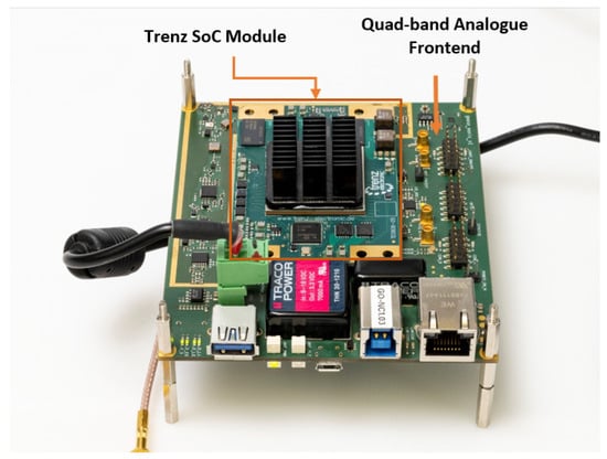
Figure 1.
GOOSE© v2 receiver platform.
The receiver architecture is based on the Commercial-Off-The-Shelf (COTS) Multi-Processor System-on-Chip (MPSoC) module designed by Trenz Electronic []. The Programmable Logic (PL) part of this device contains a Fast Fourier Transform (FFT) core, a pseudo-random noise (PRN) generator module and 60 tracking channels. The Processing System (PS) includes a quad-core 64-bit processor and implements the code/carrier tracking loops, navigation message decoding and PVT algorithm. The System-on-Chip (SoC) feature allows the exchange between HW and Software (SW) with a very high bandwidth—thanks to the on-chip communication infrastructure.
This research performs a preliminary evaluation of the GOOSE© v2 by comparing it with its legacy version, evaluating the tracking of the NavIC signals and testing the capability of managed tracking channels.
The rest of the paper is organized as follows. Section 2 describes the proposed GNSS receiver named GOOSE© v2 and addresses the main updates compared to the legacy GOOSE© v1 receiver [,]. Section 3 presents the preliminary evaluation of the GOOSE© v2. Finally, Section 4 concludes and indicates future work.
2. Receiver Design
The GOOSE© v2 GNSS receiver is composed of an analog and a digital part. The digital part is characterized by the Xilinx MPSoC composed by the PS for the processing implemented in SW and the PL, a kind of integrated Field-Programmable Gate Array (FPGA), to accelerate digital processing functions. Figure 2 shows the main architecture of the proposed platform.
Figure 2.
GOOSE© v2 architecture diagram.
2.1. Radio-Frequency Front-End
According to the targeted frequency bands, the frequency plan in Table 1 is proposed. The E5-band (including the NavIC L5) determines the maximum bandwidth of 54 MHz to enable the reception of the full Galileo E5 Alternative Binary Offset Carrier (AltBOC) signal.

Table 1.
Proposed frequency plan.
Figure 3 depicts the four-channel analog front-end of the GOOSE© v2. The input stage separates the antenna signal into four channels (see Figure 3a). After the limiter, the signal is divided into the L-band and S-band. A second diplexer is included in the L-band to split it into an upper and lower band. The lower band is connected to a splitter that creates two identical GNSS signals, which are processed separately (RF-1 and RF-2).
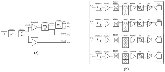
Figure 3.
Quad-band analog front-end: (a) radio frequency (RF) input stage and (b) RF signal chains.
The subsequent RF chains are processed individually (see Figure 3b). As the receiver architecture consists of one mixer stage that provides an Intermediate Frequency (IF) signal with only the real part, the pre-selection of the RF signal is important. A second measure to reduce the non-desired side bands is that the LO frequency of the mixer is higher compared to a low IF architecture with a complex IF signal. The following analog processing is performed in four different paths. After band selection and amplification, the matching network converts the signal from single-ended to differential and is optimized for each band. The mixer stage shifts the signal according to the integrated local oscillator (see Table 1). The IF bandpass filter suppresses the out-of-band signals. The voltage gain amplifier (VGA) sets the appropriate level for the Analog-to-Digital Converter (ADC). Two dual 12-bit ADCs are selected to provide good performance in the digital domain. The sampling rate of the ADC is 250 MHz and enables the digital signal conditioning to use a simple -mixer when shifting the signal to the baseband.
The schematic and the Printed Circuit Board (PCB) layout is optimized as follows:
- Same active components for all channels;
- Same footprint for all Surface Acoustic Wave (SAW) filters;
- Same structure for the matching network and the band pass filter, only the values of the components are changed.
The most significant benefit of this approach is that there is only one PCB layout design for all the channels, and the number of different active components is reduced to a minimum. This also guarantees fewer issues on the current component provisioning.
2.2. Digital Hardware Design
The digital HW board is based on a TE-0808 MPSoC module designed by Trenz Electronic []. This includes a Xilinx ZynqTM UltraScale+TM, 2 gigabyte (GB) 64-Bit Double Data Rate fourth generation (DDR4) memory, 2× Serial Peripheral Interface (SPI) Boot Flash (dual parallel) and altogether 4 × 160 pins used for the connectivity to the analog front-end board.
The benefits of employing a system on module (SoM) are the easy development, maintenance efforts and migration. On the one hand, the functionality is guaranteed by the manufacturer and it is typically possible to upgrade to an MPSoC device with a larger PL. On the other hand, they avoid the risks associated with the development of a customized FPGA board, because some special components like Random Access Memorys (RAMs) or FLASH memories cannot be bought in low volumes. The integrated SoC device is the ZynqTM UltraScale+TM XCZU15EG-1FFVC900E manufactured by Xilinx. The PS is characterized by a quad-core advanced Reduced Instruction Set Computer (RISC) machine (ARM) Cortex–A53 processor and a PL with approx. 750 K logic cells. The PL allows the implementation of real-time digital signal processing tasks at higher throughput. The firmware (FW) design mapped on the PL is described in Section 2.3.
2.3. Firmware Design
The firmware has two main purposes, i.e., to provide a signal conditioning of the received samples and to implement the different correlation methods needed by the GNSS acquisition and tracking stage. The PS of the ZynqTM controls the digital HW modules implemented in the PL by reading and writing to the control and status registers. The communication interface integrated into the ZynqTM MPSoC between PS and PL is Advanced Extensible Interface (AXI).
Baseband Design
The baseband core performs the standard GNSS operations. It contains a time management module, FFT acquisition and correlation channels for tracking. The time management module is based on a 32-bit HW counter, which runs at the frequency of the digital samples, and provides a unique time reference to all the GNSS modules.
The FFT acquisition unit is composed of a fixed size FFT core and its control logic. The acquisition supports a fast, a medium and a sensitive mode, and its algorithm is based on a parallel code-phase search method. The FFT core consists of a Xilinx XFFT Intellectual Property (IP). The size is 16 K according to the resource available on FPGA used in the platform. The acquisition module is controlled by the processor which specifies which signal should be searched for according to its acquisition strategy. Once the acquisition performs a rough estimate of the main GNSS synchronization parameters, the tracking starts and refines the estimates. In total, there are 60 correlation channels in the presented GNSS platform.
Each correlation channel supports the correlation of two components (data and pilot) of a complex input signal. For each component, up to five delayed correlation points can be produced, which means that each channel is characterized in practice by ten complex correlators. The feedback control loops (Delay Locked Loop (DLL)/Frequency Locked Loop (FLL)/Phase Locked Loop (PLL)) are implemented in SW. They read out the complex integrate-and-dump data from the HW channels through a dedicated AXI interface. The loop steering values for the carrier and code NCOs are sent back through the channel control interface.
In addition to the control part, the correlation channels are characterized by the measurement interface, which collects information about all the internal counters and is triggered by the measurement interrupt generated by the time-management module. The measurements of all the channels are performed synchronously and allow for the calculation of the time of transmission of all the signals which are currently in tracking in SW. This is needed together with the time of arrival for the PVT calculation.
2.4. Software Design
The ogre_console is the main receiver program which manages the GNSS acquisition, tracking and PVT calculation processes. According to the signals selected (frequency and constellation), the receiver SW performs the acquisition in a continuous loop. For each acquired signal, a correlation channel is started. Different tracking options for each signal can be specified. As soon as enough signals are in tracking, a PVT can be calculated. The PVT is based on code measurements from the channels and the decoded Ephemeris.
3. Preliminary Receiver Evaluation
3.1. Resource Utilization on PL FPGA
Table 2 shows the resource utilization of the GOOSE© v2 receiver compared to v1. Since the same FFT size and amount of tracking channels are instantiated (as shown in Table 3), there is no significant difference in slice Lookup Tables (LUTs) between the two implementations. The 20,000 more LUTs are associated with the additional frequency band added in the digital signal conditioning. Each ADC frequency channel is first down-converted using the -mixer and then down-sampled with a factor of 4. Therefore, an additional static Low-Pass Filter (LPF) is needed for anti-aliasing. This significantly increases the amount of Digital Signal Processor (DSP) blocks used, which is still only 10% of the blocks available on the device.
Table 2.
Resource utilization.
Table 3.
Firmware design components and properties.
3.2. Performance Comparison between GOOSE v1 and GOOSE v2
In order to test the communication aspect of HW and SW, a parallel test with GOOSE© v1 and GOOSE© v2 is conducted in our Galileo lab using the Spirent Radio-Frequency Constellation Simulator (RFCS). The aim is to find out the number of tracking channels that the GNSS receiver can handle. The test setup is presented in Figure 4. Here, the RF output of the Spirent is connected to both receivers through a splitter.
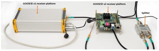
Figure 4.
Test setup.
The selected test scenario includes GPS L1/L5 and Galileo E1/E5a signals. The HW integration time is set to 1 ms for both receiver platforms. Figure 5 shows the result of this test. At the start of the scenario, five SVs are enabled. Afterwards, one SV is added with at 1 min intervals. The number of tracked HW channels increases with respect to time. The trend is similar in both platforms, until E11 is added at the 480th second, where all of a sudden, the GOOSE© v1 stops while the other keeps tracking more SVs.
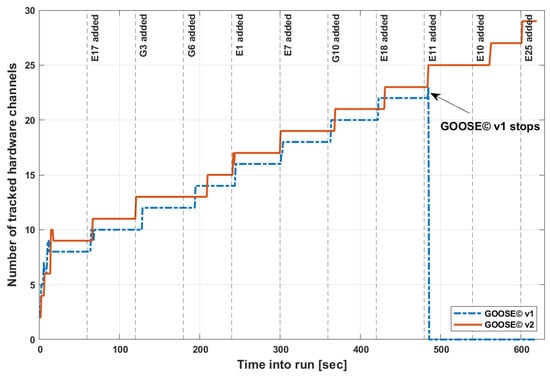
Figure 5.
GOOSE© v1 and GOOSE© v2 performance result.
Figure 6 presents the computational load of both receivers at the break point of GOOSE© v1. Due to the high time complexity of the communication interface between PL and PS, the GOOSE© v1 cannot close the tracking channels in less than 1 ms. Consequently, the receiver SW application increases the computational load to a level until it terminates.
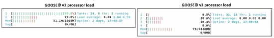
Figure 6.
GOOSE© v1 and GOOSE© v2 processor load.
This result shows that GOOSE© v2 outperforms the GOOSE© v1 receiver when the HW integration time is reduced to 1 ms. This aspect plays a vital role for algorithms where the tracking loops need to be closed in the lowest possible time, such as in Vector Tracking (VT) [], Deep Coupling (DC) and LBCA [].
3.3. NavIC Tests Using GOOSE v2
The proposed platform was designed to support the NavIC processing. NavIC is a regional navigation satellite established by Indian Space Research Organization (ISRO). It is designed with a constellation of seven satellites and a network of ground stations. Currently, three satellites are placed in geostationary orbits and four satellites are placed in inclined geosynchronous orbits [].
The first test demonstrates that the platform can acquire and track the L5 band of all the NavIC satellites visible from the test facility. The test setup is composed of GOOSE© v2 connected to the NavIC reference antenna. The NavIC reference antenna is mounted on the roof of the Fraunhofer IIS building in Nuremberg. Figure 7 shows that four L5 signals are acquired and are in stable tracking with a carrier-to-noise density ratio () of approx. 40 dBHz.
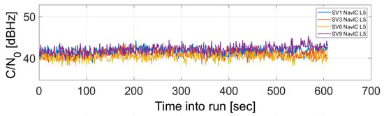
Figure 7.
NavIC-L5 results using GOOSE© v2.
Table 4 shows a comparison of the between the proposed platform and a commercial receiver (Septentrio Mosaic-X5 []). The lower of the GOOSE© v2 might be due to the larger reception bandwidth, which also causes unwanted signals being processed. In order to improve the , some additional filtering is needed in the S band channel or some interference mitigation capability.
Table 4.
NavIC-L5 mean values comparison between GOOSE© v2 and Mosaic-x5 receiver.
3.4. L1–L5 Tests Using GOOSE v2
To evaluate the more commonly used GPS and Galileo constellations, an additional test was performed. GPS L1CA and L5, Galileo E1BC and E5 AltBOC, and NavIC L5 and S were tracked using the NavIC reference antenna. In parallel, Septentrio PolaRx5 receivers also track signals of the same constellations. Figure 8a,b show the results of the GPS L1CA and Galileo E1BC using the GOOSE© v2. The results of the same signals using Septentrio PolaRx5 are provided in Figure 9. Here, we can see a slight difference in the amount of signals tracked due to the higher sensitivity of the commercial receiver.
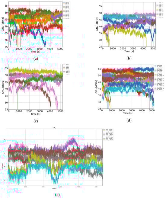
Figure 8.
results with GOOSE© v2. (a) GPS L1, (b) Galileo E1, (c) GPS L5, (d) E5 AltBOC and E5A, and (e) NavIC L5 and S.
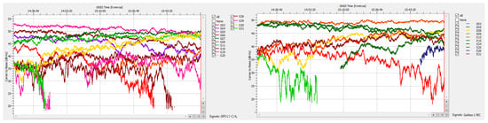
Figure 9.
GPS L1 and Galileo E1 results using Septentrio PolaRx5.
Figure 8c,d show the results of the GPS L5 and Galileo E5 AltBOC on the GOOSE© v2. The results of the same signals using Septentrio PolaRx5 are provided in Figure 10. In this case, the of the two platforms is comparable and the same signals are tracked. No relevant difference can be observed for the L5-E5 band.
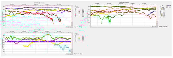
Figure 10.
GPS L5 and Galileo E5 AltBOC results using Septentrio PolaRx5.
In addition, Figure 8e shows the for the NavIC L5- and S-band tracked satellites. The Septentrio receiver can track one low- signal more but cannot track signals in the S band.
In the test, we can see that both frequencies can be tracked for all the satellites except SVID1. The reason for this is not clear and should be further investigated. Additionally, L5 provides a higher of up to 3 to 5 dBHz. This could be due to the presence of interfering signals in the S band.
4. Conclusions
This paper presents an enhanced version of the legacy GOOSE©, the GOOSE© v2. This new platform is an MPSoC-based GNSS receiver that contains a quad-band (L1, L2, L5/E5 and S band) Radio-Frequency Front-End (RFFE) and baseband digital signal processing. The SoC feature allows at the same time the exchange between HW and SW with a very high bandwidth—thanks to the on-chip communication infrastructure. The results show that, in addition to the legacy signals, the new receiver platform supports the NavIC L5 and S-band signals along with the ability to close the tracking loops faster than its previous version. In addition, the proposed platform includes a Coral accelerator module suitable for exploiting potential GNSS Machine Learning (ML) algorithms [].
As future work, the testing of the digital record and replay capability of the GOOSE© v2 using the four channels will be performed. In addition, the High-rate DFT-based Data Manipulator (HDDM) will be implemented in the PL of the platform []. Moreover, due to low time complexity of the PL-PS communication interface, more complex algorithms will be evaluated in SW, such as the VT and the LBCA.
Author Contributions
Conceptualization: F.G. and F.F.; Methodology: F.F. and S.U.; Software: S.-J.W. and M.S.; Validation: M.S., S.U. and F.G.; Formal analysis: F.F., I.C. and F.G.; Investigation: F.F. and M.S.; Writing—original draft preparation: M.S.; Writing—review and editing: M.S., I.C., S.-J.W., F.F. and M.O.; Visualization: S.-J.W. and F.G.; Project administration: M.S., M.O.; Funding acquisition: W.F. All authors have read and agreed to the published version of the manuscript.
Funding
Parts of the work presented in this paper are funded by the European Space Agency (ESA) Navigation Innovation and Support Program (NAVISP) Element 2 project “GOOSE-NavIC”, which is managed by TeleOrbit GmbH (TOG) (ESA Contract No.: 4000137080/22/NL/MP/mk).
Institutional Review Board Statement
Not applicable.
Informed Consent Statement
Not applicable.
Data Availability Statement
The data presented in this study are available from the corresponding author on request. The data are not publicly available due to its data size and further explanations may be needed.
Acknowledgments
We acknowledge ESA and TOG for their valuable contributions, interest and time. We are also thankful to Gupta, Himanshu and Dietmayer, Katrin for the results analysis and review process. We also want to express our gratitude to Karim, Abrarul for the help in preparing the test setup.
Conflicts of Interest
The authors declare no conflict of interest. The funders had no role in the design of the study; in the collection, analyses, or interpretation of data; in the writing of the manuscript; or in the decision to publish the results.
References
- European Union Agency for the Space Programme (EUSPA). EUSPA EO and GNSS Market Report; Market Report Issue 1; European Union Agency for the Space Programme (EUSPA): Luxembourg, 2022. [Google Scholar]
- Overbeck, M.; Garzia, F.; Popugaev, A.; Kurz, O.; Forster, F.; Felber, W.; Ayaz, A.S.; Ko, S.; Eissfeller, B. GOOSE–GNSS Receiver with an Open Software Interface. In Proceedings of the 28th International Technical Meeting of The Satellite Division of the Institute of Navigation (ION GNSS 2015), Tampa, FL, USA, 14–18 September 2015. [Google Scholar]
- Cortes, I.; Van der Merwe, J.R.; Rügamer, A.; Felber, W. Adaptive loop-bandwidth control algorithm for scalar tracking loops. In Proceedings of the IEEE/ION PLANS, Portland, OR, USA, 20–23 April 2020. [Google Scholar]
- Cortés, I.; van der Merwe, J.R.; Nurmi, J.; Rügamer, A.; Felber, W. Evaluation of Adaptive Loop-Bandwidth Tracking Techniques in GNSS Receivers. Sensors 2021, 21, 502. [Google Scholar] [CrossRef] [PubMed]
- Cortés, I.; van der Merwe, J.R.; Lohan, E.S.; Nurmi, J.; Felber, W. Evaluation of Low-Complexity Adaptive Full Direct-State Kalman Filter for Robust GNSS Tracking. Sensors 2023, 23, 3658. [Google Scholar] [CrossRef] [PubMed]
- UltraSOM+ MPSoC-Modul mit Zynq™ UltraScale+™ XCZU15EG-1FFVC900E, 4 GB DDR4. Available online: https://shop.trenz-electronic.de/de/TE0808-05-BBE21-A-UltraSOM-MPSoC-Modul-mit-Zynq-UltraScale-XCZU15EG-1FFVC900E-4-GB-DDR4 (accessed on 5 May 2023).
- Garzia, F.; Strobel, C.; Overbeck, M.; Kumari, N.; Joshi, S.; Förster, F.; Felber, W. A multi-frequency multi-constellation GNSS development platform with an open interface. In Proceedings of the 2016 European Navigation Conference (ENC), Helsinki, Finland, 30 May–2 June 2016; pp. 1–7. [Google Scholar] [CrossRef]
- Seybold, D. GOOSE: Open GNSS Receiver Platform. Technical Report. TeleOrbit GmbH, 2020. Available online: https://teleorbit.eu/en/satnav/goose/ (accessed on 14 May 2023).
- Dietmayer, K.; Saad, M.; Strobel, C.; Garzia, F.; Overbeck, M.; Felber, W. Real time implementation of Vector Delay Lock Loop on a GNSS receiver hardware with an open software interface. In Proceedings of the 2019 European Navigation Conference (ENC), Warsaw, Poland, 9–12 April 2019; pp. 1–7. [Google Scholar] [CrossRef]
- ISRO. Indian Regional Navigation Satellite System: Signal in Space ICD for Standard Positioning Service (Version 1.1); Indian Space Research Organization: Bengaluru, India, 2017.
- Septentrio Mosaic-X5 Development Kit. Available online: https://shop.septentrio.com/en/shop/mosaic-x5-devkit (accessed on 14 May 2023).
- Accelerator Module: A Solderable Multi-Chip Module Including the Edge TPU. Available online: https://coral.ai/products/accelerator-module (accessed on 1 July 2022).
- Garzia, F.; van der Merwe, J.R.; Rügamer, A.; Urquijo, S.; Felber, W. HDDM Hardware Evaluation for Robust Interference Mitigation. Sensors 2020, 20, 6492. [Google Scholar] [CrossRef] [PubMed]
Disclaimer/Publisher’s Note: The statements, opinions and data contained in all publications are solely those of the individual author(s) and contributor(s) and not of MDPI and/or the editor(s). MDPI and/or the editor(s) disclaim responsibility for any injury to people or property resulting from any ideas, methods, instructions or products referred to in the content. |
© 2023 by the authors. Licensee MDPI, Basel, Switzerland. This article is an open access article distributed under the terms and conditions of the Creative Commons Attribution (CC BY) license (https://creativecommons.org/licenses/by/4.0/).