Abstract
A screen-printed electroluminescent (EL) matrix display on fabric is presented. This work demonstrates the fabrication of a screen-printed multilayer display with a matrix of 8 × 8 pixels, as well as the design and construction of integrated drive electronics capable of operating the EL display and achieving good visibility. Each pixel is 1 mm × 1 mm, which is smaller than in previously reported literature. The EL matrix was successfully printed and laminated on fabric at this higher resolution, improving the visual effect and decreasing the overall display size, and reducing the impact on the flexibility and breathability of the underlying fabric. This proof-of-concept demonstrator EL display shows the potential for more complex pixel displays for e-textile and printed electronic applications, such as interactive clothing, and information displays in applications, such as the automotive field, architecture, and point of sale advertising.
1. Introduction
Printed electroluminescence (EL) materials are widely used for the fabrication of long-lasting, high-intensity light-emitting devices on flexible substrates [1]. The main benefits are the ease of fabrication of an EL multilayer structure via screen printing, which has a higher layer-thickness tolerance compared with equivalent printed OLEDs. In addition, the polymer inks required for fabrication are more widely available. The previous literature has successfully implemented an EL display on fabrics to fabricate a watch [2] and a traffic signal system on a backpack [1]. To achieve improved high-resolution display performance, the pixel pitch, which is the distance from the centre of a pixel to the centre of the adjacent pixel, is a critical dimension. A lower pixel pitch results in an image with smoother edges, finer detail, and smaller dimensions in the flexible display, increasing the comfort of wearable e-textile applications.
2. Materials and Methods
2.1. Electroluminescent (EL) Lamp Structure
A standard parallel plate capacitor configuration is used to make EL lamps, with a light-emitting phosphor layer sandwiched between the two electrodes. To allow light to be emitted, one of the electrodes is transparent. Because the phosphor layer would electrically break down at high field strengths, a dielectric layer is also placed between the electrodes to prevent a short circuit. Figure 1 shows the cross-section structure of a complete EL lamp with the materials used for each layer, which consists of four layers [2]. A bus-bar layer is added between the phosphor and the translucent conductor (PEDOT) layer for improved electric field distribution in this design to create an 8 × 8 pixels array.
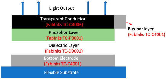
Figure 1.
Schematic diagram of the cross-section structure of printed EL lamp with inks used from Smart Fabric Inks Ltd. for each layer, which are labelled in red.
2.2. EL Pixel Arrays Fabrication
The screen-printing method was used to print the flexible EL lamps array with high printing resolution and low cost compared with the clean room facilities typically required for OLED production.
2.2.1. Screen Design
The first step of printing EL lamps is manufacturing the screen. In this project, to test the resolution limitation of screen-printing method, two layouts for the displays were designed using Tanner L-Edit software. The screen design is shown in Figure 2A, which has a print area of 10 cm × 10 cm. It consists of seven large pixel arrays (one of which is labelled with the red shaded area in Figure 2A) and eight combinations of nine small pixel arrays (one of which is labelled with the blue shaded area in Figure 2A), plus six alignment patterns to aid registration of the various layers in the printing process. The screen details (mesh size and emulsion thickness) are given below for each layer.
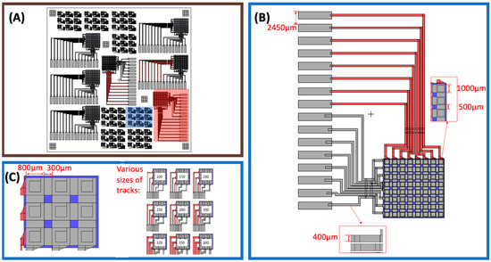
Figure 2.
Screen design, which consists of overall layout (A), larger 8 × 8 pixels arrays, (B) and smaller 3 × 3 pixels arrays (C).
In the large pixel 8 × 8 array, the size of each pixel is 1000 μm × 1000 μm with a gap of 500 μm, which is shown in Figure 2B. The linewidth of the connecting tracks is 500 μm, while the width of the connector pitch is 2540 μm to match the flexible printed circuit (FPC) connector used for testing.
The smaller pixel arrays were designed to test the resolution limits of the screen printing. The size of each pixel in the 3 × 3 pixels arrays is 800 μm × 800 μm, with a gap of 300 μm (Figure 2C, left part). The sizes of the connecting tracks of nine different arrays were designed to vary from 100 microns to 400 microns, which is shown in Figure 2C (right part), to explore the printing resolution limitation of screen-printing method.
2.2.2. Screen Printing Process
The EL lamps array was fabricated using five functional layers as detailed below. The schematic pictures of the patterns after printing each layer are shown in Figure 3. A 120-34 polyester screen with 5 μm emulsion thickness was used for each screen except for the busbar, which had 30 μm emulsion to aid the print step across the layers, and the PEDOT layer, which used a 140-30 mesh, identified as the optimum mesh by the ink manufacturer.
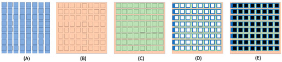
Figure 3.
Top views of the EL lamps after the printing of each layer: (A) silver layer, (B) dielectric layer, (C) phosphor layer, (D) bus-bar layer, (E) PEDOT layer.
The printing process used to produce the EL lamp is:
- Print silver layer to create the conductive tracks and conductive pads. The paste was cured in a box oven at 120 °C for 10 min;
- Print dielectric layer to prevent short circuit across the capacitor structure and acts as a light reflector. The paste was cured at 130 °C for 15 min;
- Print phosphor light-emitting layer. The paste was cured at 130 °C for 15 min;
- Print busbar layer to create conductive tracks and conductive pads. The paste was cured at 120 °C for 15 min;
- Print PEDOT layer to allow light emission from the phosphor layer. The paste was cured at 130 °C for 15 min.
3. Results and Discussions
The EL pixels arrays were printed on 120 μm Policrom film and then laminated on to the fabric to achieve the flexible EL display screen on the fabric. The lamps were tested using a standard EL driving circuit, shown in Figure 4, which shows the visibility of each pixel and the retained flexibility of the fabric.
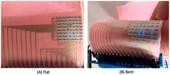
Figure 4.
Powering the larger EL pixels arrays in flat (A) and bent (B) conditions.
The optical properties of the blue emitter were also assessed, which is shown in Figure 5A. The emission peak is at a wavelength of ~550 nm, with a brightness of ~200 cd/m2. The detected colour of emitting light was shown in CIE 1931 colour space in Figure 5B, of which the coordinates are (0.156, 0.426).
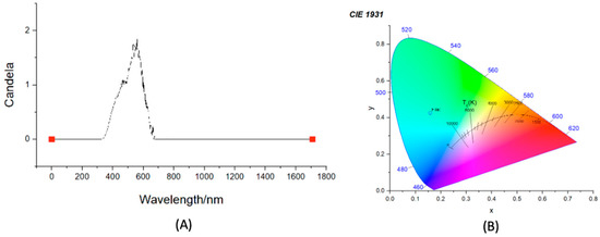
Figure 5.
Measured luminance (A) and CIE 1931 colour space (blue circle) (B).
The smaller 3 × 3 pixels arrays were also tested, and the arrays of sizes greater than or equal to 150 μm were successful. There were defects in the printed 100-microns tracks, which caused open circuits, meaning the pixels could not be lit up. The printed performance of nine different sizes of tracks indicates that the screen-printing method is suitable for fabricating devices with track widths of more than 150 μm.
4. Conclusions
This work improved the screen-printed resolution of electroluminescent (EL) lamps on fabric and is capable of reducing the size of displays whilst retaining the flexible property of fabrics, which helps in reducing the size limit of wearable display devices. However, the limitation is that the screen-printing resolution must be 150 μm to achieve operational displays. Thus, future work must investigate an alternative printing method, namely reverse-offset printing, and use it to fabricate EL lamps to reduce their size by a factor of at least two whilst maintaining good performance.
Author Contributions
H.D. carried out the experiment design and implementation and wrote the manuscript draft. T.G. provided technical support in building the driving circuit. R.T. provided supervision for the research work, screen design, material selection, and electronics and edited the manuscript draft. S.B. supervised the research and edited the manuscript draft. All authors have read and agreed to the published version of the manuscript.
Funding
This work was supported by EPSRC grant Wearable and Autonomous Computing for Future Smart Cities: A Platform Grant (EP/P010164/1).
Institutional Review Board Statement
Not applicable.
Informed Consent Statement
Not applicable.
Data Availability Statement
No new data were created or analyzed in this study. Data sharing is not applicable to this article.
Conflicts of Interest
The authors declare no conflict of interest.
References
- Ivanov, A. A printed electroluminescent matrix display: Implementation details and technical solutions. In Proceedings of the 2018 IMAPS Nordic Conference on Microelectronics Packaging (NordPac), Oulu, Finland, 12–14 June 2018. [Google Scholar] [CrossRef]
- de Vos, M.; Torah, R.; Glanc-Gostkiewicz, M.; Tudor, J. A Complex Multilayer Screen-Printed Electroluminescent Watch Display on Fabric. J. Disp. Technol. 2016, 12, 1757–1763. [Google Scholar] [CrossRef]


Disclaimer/Publisher’s Note: The statements, opinions and data contained in all publications are solely those of the individual author(s) and contributor(s) and not of MDPI and/or the editor(s). MDPI and/or the editor(s) disclaim responsibility for any injury to people or property resulting from any ideas, methods, instructions or products referred to in the content. |
© 2023 by the authors. Licensee MDPI, Basel, Switzerland. This article is an open access article distributed under the terms and conditions of the Creative Commons Attribution (CC BY) license (https://creativecommons.org/licenses/by/4.0/).