Abstract
CZTS (C-I/C-II) ultrathin films in 61 nm and 313 nm thicknesses were grown on microscopic glass and n-Si wafer substrates via laser ablation, respectively. C-II ultrathin film with higher thickness has a more developed crystal structure and consists of larger particles compared to C-I ultrathin film with reduced thickness. C-II ultrathin film absorbs more photons and has a lower band gap. The photovoltaic performance of the produced Ag/CZTS (C-II)/n-Si/Al solar cell is higher compared to the other solar cell-based C-I ultrathin film. The more improved crystal structure of C-II ultrathin film has increased the efficiency of the solar cell. The calculated photovoltaic parameters of the solar cells modeled with the SCAPS-1D simulation program were found to be compatible with the experimental parameters. This situation has proven that the operating performance of solar cells is reliable.
1. Introduction
Cu2ZnSnS4 (Copper Zinc Tin Sulfide) material, one of the second-generation solar cells, attracts attention because it has p-type semiconductor electrical conductivity, a high absorption coefficient (>104 cm−1), an adjustable band gap between 1 and 1.5 eV, and environmental friendliness; it is also composed of elements that are abundant in the environment [1,2,3]. These features of CZTS (Cu2ZnSnS4) make it stand out compared to CdTe (Cadmium Tellur) and CuInGaSe2 (Copper Indium Gallium Selenide) solar cells, which consist of toxic and expensive elements [4]. In general, CZTS second-generation solar cells (SGSC) include Mo-(Molybdenum)/p-CZTS/n-CdS-(Cadmium Sulfide)/i-ZnO-(intrinsic Zinc Oxide)/ITO-(Indium–Tin Oxide) thin film layers. However, these layers are produced with different coating techniques and each layer goes through a long and difficult production process. Cracks, pinholes, defects, and traps that can occur in thin films due to environmental and production conditions during the deposition of many layers on top of each other adversely affect the solar cell’s performance [5,6]. In addition, it contains toxic Cd (Cadmium), an element which is dangerous to human health [7]. At this point, n-Si (Silicon wafer)/p-CZTS solar cells have the advantages of ease of production, a short production time, environmental friendliness, and stable film growth [8,9,10,11]. Moreover, since the crystal lattice constants of the CZTS material (a = 0.5427 nm/c = 1.0848 nm) and the Si semiconductor (a = 0.5430 nm) are close to each other, the lattice mismatch between the two semiconductors is low [12] and CZTS thin film can be produced epitaxially on Si wafer [13]. Thus, the formation of interface states, dangling bonds, defects and traps between the p-n junction is limited and more charge is accumulated at the boundaries of the depletion region, thus increasing the Voc (open-circuit voltage) and Jsc (short-circuit current density) values.
Solar cell modeling is performed using SCAPS-1D (One-dimensional Solar Cell Capacitance Simulator software) to determine and verify the operating performance of solar cells [11,14]. A functional study can be carried out on the modeled solar cell PV (photovoltaic) performance depending on parameters such as the operating temperature, interface defect density, acceptor/donor defect density, and Auger electron/hole capture coefficient. While calculating the PV parameters of solar cells consisting of different layers, the effects of the electrical, optical, and defect structures of the layers on the PV performance can be revealed [15].
The PLD (Pulse Laser Deposition) technique was used to fabricate the CZTS/n-Si heterojunction solar cell in this study. PLD is a very advantageous technique for the stoichiometric transfer of multi-element complex materials and for the growth of qualified epitaxial and crystalline, homogeneous ultrathin films under high-vacuum conditions. The ultrathin films (with thickness below 500 nm) [15,16] with desired morphological, electrical, optical, and crystalline properties can be produced by adjusting the laser wavelength, fluency, pulse number, and background gas pressure [17,18,19,20]. In particular, epiaxial CZTS ultrathin film growth on Si wafer with PLD is achieved with high success [16].
In this study, we ablated CZTS material with two different laser pulse numbers and grew their ultrathin films. Ag/CZTS (C-I and C-II)/n-Si/Al heterojunction solar cells were produced with these two thin films whose morphological, crystalline and optical properties were examined. The solar cells with measured PV parameters were modeled using SCAPS-1D simulation software. The experimental and theoretical PV parameters for two solar cells are compatible and the operating performances of the solar cells have been verified. A simulation study has been carried out depending on the acceptor defect density in the CZTS semiconductor, operating temperature, and interface defect density.
2. Materials and Methods
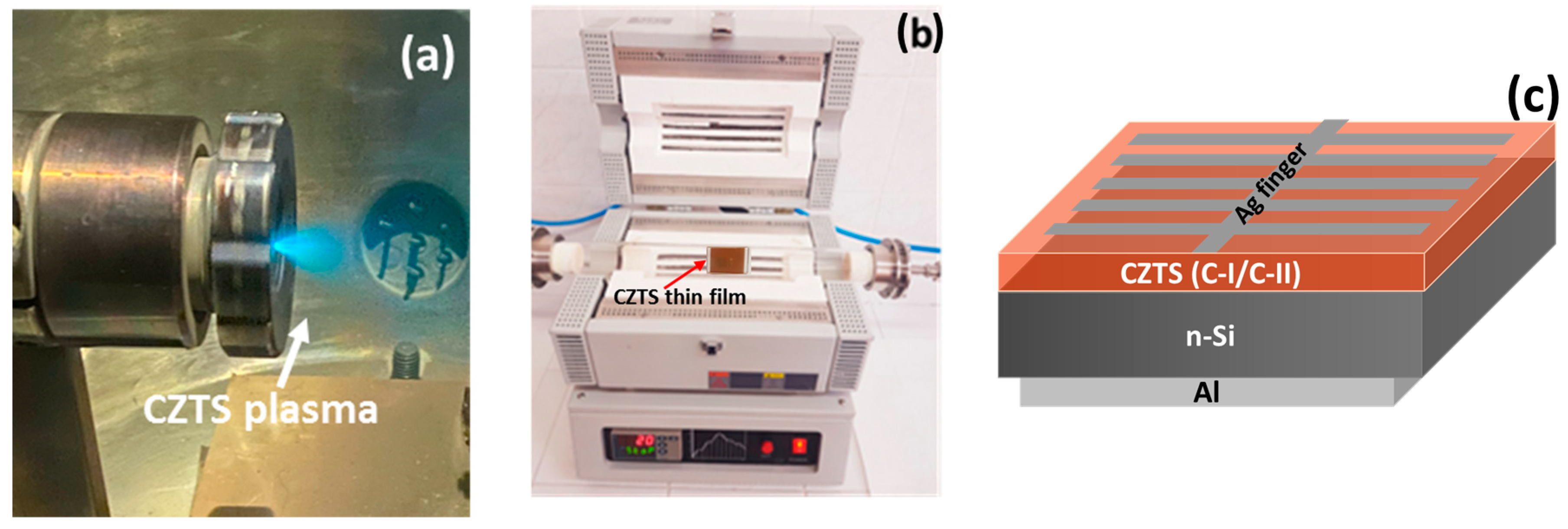
The laser beam (Continuum Minilite NdYAG laser; Electro-Optics, Inc.; Santa Clara; CA; USA (1064 nm wavelength, 15 mJ laser energy, 10 Hz repetition rate, 5 ns pulse width)) with two different laser pulse numbers ablated the CZTS sputtering target and the CZTS species deposited separately on the microscopic glass and n-Si wafer substrates at room temperature under 1 × 10⁻⁶ mbar of vacuum pressure. A photograph of the plasma formed by laser beam ablation is shown in Figure 1a. The procedure used to clean the substrates was described in our previous study [16]. The CZTS ultrathin films produced with 2.400 and 12.000 laser pulse number are named C-I and C-II. Afterwards, these ultrathin films were placed next to 50 mg of powder and annealed in a vacuum environment at 375 °C temperature, as seen in Figure 1b.

Figure 1.
(a) Plasma photography of CZTS material ablated with laser beam. (b) Photo of CZTS thin film to be annealed in quartz tube furnace. (c) Schematic view of Ag/CZTS (C-I/C-II)/n-Si/Al heterojunction solar cell.
Solar cell production stages: CZTS ultrathin films were grown on the shiny side of the n-Si wafer (10 Ω.cm resistance/1 cm2 area/(100)crystalline orientation/500 µm thickness) as mentioned above. Then, using the PVD technique, Al metal contact was deposited on the matte side of the Si wafers and the annealing process was carried out. Finally, the Ag/CZTS/n-Si/Al solar cell structure shown in Figure 1c was formed by depositing Ag finger metal contacts on the CZTS ultrathin films using a specially prepared mask.
XRD (X-ray Diffraction; Bruker AXS, Karlsruhe, Germany), HR-TEM (high-resolution transmission electron microscopy; JEOL Ltd., Tokyo, Japan), a UVvis (ultraviolet–visible; JASCO, V-670, Waltham, USA) spectrophotometer, and SEM (Scanning Electron Microscopy; ZEISS, Oberkochen, Germany) analysis techniques were used to investigate the morphological, optical, and crystalline properties of the CZTS ultrathin films. Ag/CZTS/n-Si/Al heterojunction solar cells were modeled by inputting the electrical and optical properties of C-I and C-II ultrathin films into the SCAPS-1D simulation program. The reliability of the photovoltaic values of the produced solar cells was verified by calculating the photovoltaic parameters of Jsc, Voc, FF (Fill Factor), and η (power conversion efficiency).
3. Results and Discussion
3.1. Results
The crystal structure of C-I and C-II ultrathin films is shown in the crystal pattern in Figure 2. The thin films are crystallized in (112), (200), and (220) orientations on angles, respectively, and have a tetragonal and polycrystalline crystal structure [21,22]. The C-I ultrathin film deposited with low laser pulse number has a weak crystal structure. While the main peak intensity in the (112) orientation is very low, the peak intensity of the (200) crystal orientation is high due to the low formation energy. As the deposition rate of atoms ablated from the CZTS sputtering target that increased with high laser pulse numbers, the atoms arranged more ideally, improving C-II ultrathin film’s crystal structure and the intensity of the main peak increased significantly [23]. The minority charge carriers in the more developed crystalline C-II ultrathin film are less likely to recombine in defects and traps, resulting in higher charge lifetimes.
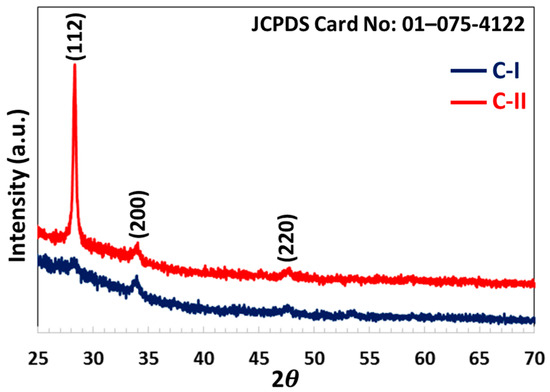
Figure 2.
XRD pattern of C-I and C-II ultrathin film.
The ultrathin film crystallite size has been calculated using the Scherrer equation () [15]. D = crystalline size; β = the full width at half-maximum of diffraction peak; λ = X-ray wavelength; θ = Bragg diffraction angle. The calculated crystallite sizes of C-II and C-I ultrathin films are 22.25 nm and 7.34 nm (Table 1), respectively. Since the enhancement in the laser pulse number augments the number of deposited atoms, the high number of regularly arranged atoms causes an expansion in the crystal size [23].

Table 1.
Thickness and crystal size values of C-I and C-II ultrathin films.
3.2. TEM and SEM Property
The HR TEM image in Figure 3 indicates that the CZTS ultrathin film has a developed crystal orientation. The space between the crystal orientations was determined as 0.31 nm [24]. SEM images in Figure 4a,b show that the particle sizes and numbers forming the C-II ultrathin film are larger and denser than those of C-I. The number of atoms deposited side by side and on top of each other, which increases with augmentation laser pulse numbers, and this causes the atoms deposited on the substrate to combine with each other, leading to an expansion in the particle size [15,16,25,26]. The ultrathin films are composed of partially inhomogeneous particle. Since the number of deposited atoms is higher and the particle size is large, the thickness of the C-II-ultrathin film is upward of than that of C-I, and the thickness of C-II thin film is shown in the SEM cross section image in Figure 3b.
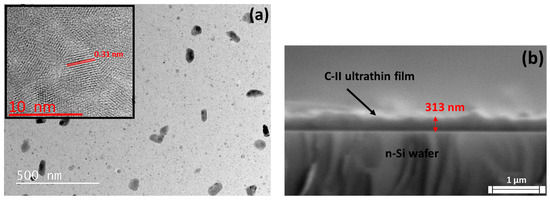
Figure 3.
(a) TEM and HR-TEM (insert square) images of CZTS ultrathin film and (b) SEM cross section image of C-II ultrathin film.

Figure 4.
EDX spectra and SEM (insert square) images of (a) C-I and (b) C-II ultrathin films.
The EDX Spectra in Figure 4 and Table 2 that show the elements’ atomic weight ratios that form the C-I and C-II ultrathin films. These ultrathin films are Sn and Zn rich, Cu poor [27,28]. While CZTS sputtering targets are ablated with low laser energy, the amount of Cu is slightly low in the ultrathin films due to the possibility of the laser fluency remaining below the Cu threshold value [27]. The amount of Sn was determined to be slightly higher because the Sn element atoms diffused to the ultrathin film surface to evaporate at the annealing temperature of 375 °C [29]. However, the ultrathin film’s stoichiometric structure developed with the high in film thickness and a more ideal composition ratio was approached.

Table 2.
The elements’ atomic weight ratios in C-I and C-II ultrathin films.
3.3. Optical Property
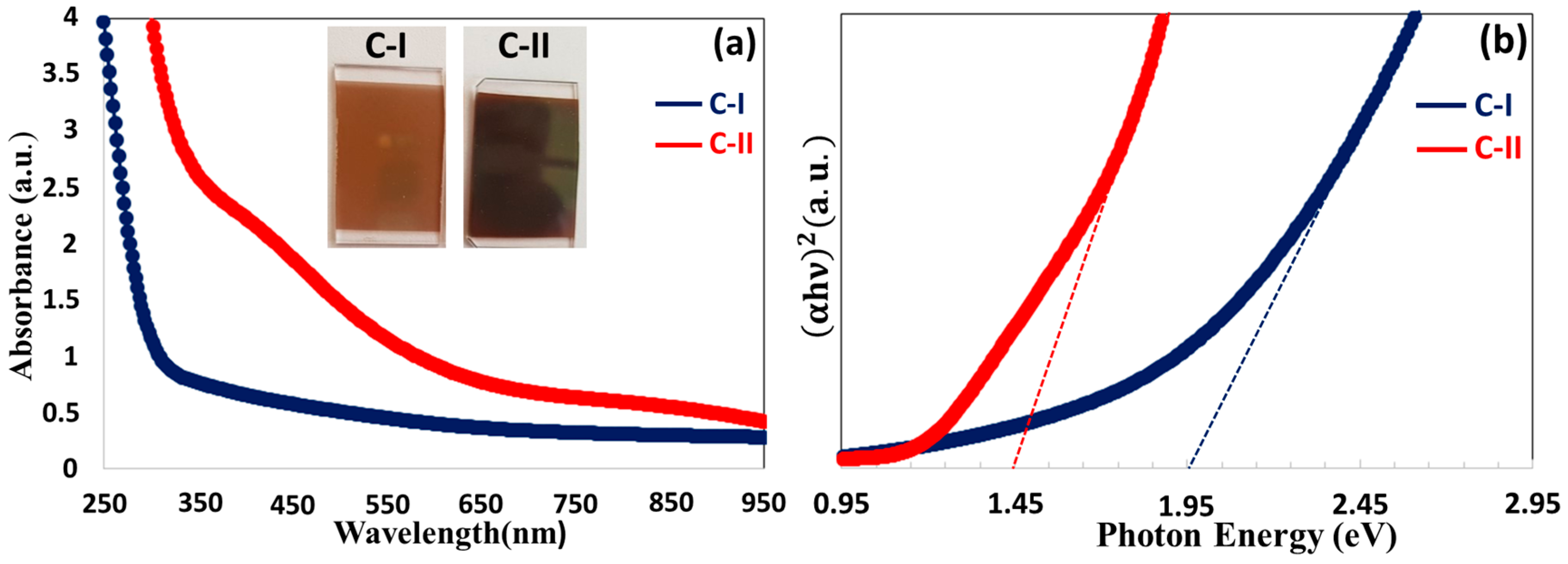
C-II ultrathin film has higher photon absorption from UV to visible region compared to C-I, in the absorption graph in Figure 5a. Since the C-II thin film consists of larger particles and has a higher thickness, it absorbs a higher amount of photons and is darker in color (insert square in Figure 5a). In contrast to this situation, C-I, which is more transparent in color, has low photon absorption due to its low thickness [15,16]. The band gaps () of C-I and C-II ultrathin films, which were found to be 1.95 eV and 1.45 eV from the energy band graph obtained using the Tauc equation of [15], respectively. The high-photon absorbing C-II ultrathin film is in the lower band gap and has suitable optical properties to employ as an absorber layer of solar cells.

Figure 5.
(a) Absorption spectrum (the photographs of C-I and C-II ultrathin film at insert square) and (b) Tauc plot graphs of C-I and C-II ultrathin films.
3.4. Modeling of Ag/CZTS/n-Si/Al Heterojunction Solar Cell and Calculation of Photovoltaic Parameters Using SCAPS-1D Simulation Software
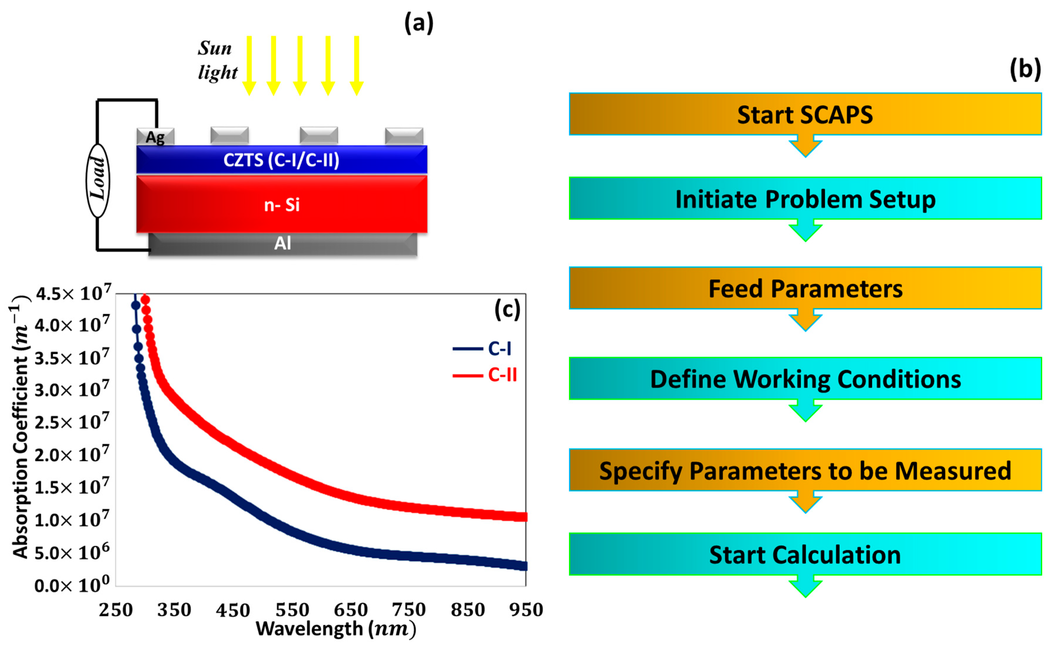
In this study, C-I and C-II solar cells were modeled and PV parameters were computed by using SCAPS-1D [11,14] and the work steps in Figure 6a,b. The physical parameters of C-I and C-II ultrathin film semiconductors in Table 3 were input into the program to perform modeling. The absorption coefficients () of ultrathin films were calculated using equation [30,31] (: absorption; : thickness) and (α) vs. wavelength spectra were plotted in Figure 6c.

Figure 6.
(a) Ag/CZTS (C-II)/n-Si/Al solar cell diagram; (b) working steps of SCAPS-1D simulation program; (c) absorption coefficient spectra of C-I and C-II ultrathin film.

Table 3.
The physical parameters of n-Si semiconductor, C-I and C-II ultrathin films.
Comparative curves of experimentally measured and theoretically calculated PV parameters of C-I and C-II solar cells are given in Figure 7. Theoretical/experimental PV data of these solar cells are presented in Table 4. The experimental/calculated data are found to be somewhat close to each other, which shows that the solar cells operate reliably [11,15,16,32]. According to the experimental parameters, the efficiency of the C-II solar cell is much higher than that of the C-I solar cell. The improved crystal structure of the C-II thin film indicates that the number of grain boundaries and the number of traps and defects in the CZTS thin film are lower. Therefore, since the lifetime of the minority charge carriers in the C-II-ultrathin film is longer, charge transitions also occur easily. Thus, the charge accumulation in the contact areas at the boundaries of the depletion region increases, resulting in an enhancement in Voc and Jsc values. Some functional studies have been carried out on C-II solar cells, and several such studies are described below.

Figure 7.
The experimental/theoretical characteristics of (a) C-I and (b) C-II solar cells.

Table 4.
The calculated and experimental PV parameters of C-I and C-II solar cells.
3.4.1. The Effect of Radiative Recombination Coefficient (Br) in CZTS (C-II) Ultrathin Film
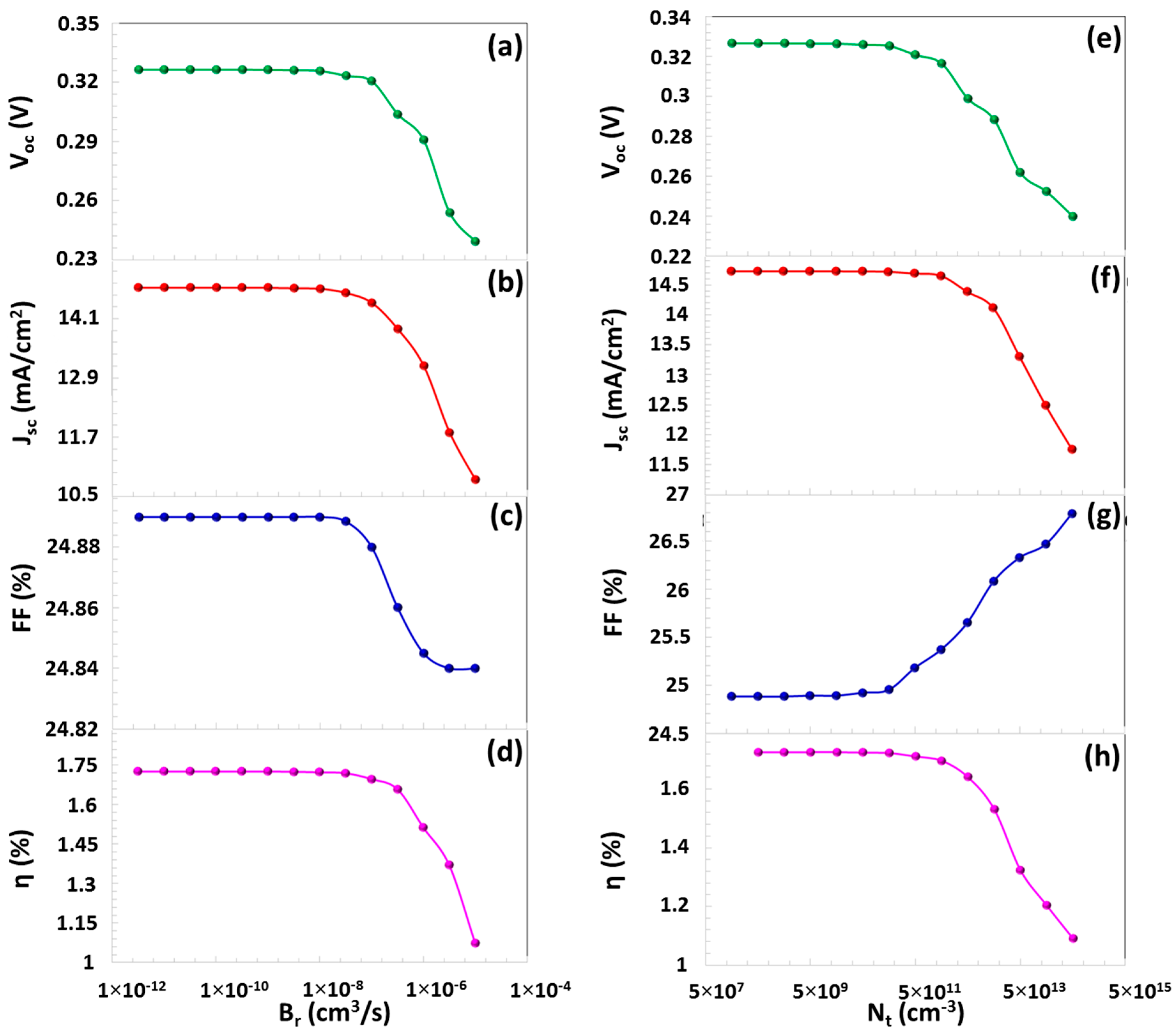
The radiative recombination in CZTS (C-II) ultrathin film negatively affects the Jsc and Voc parameters of the solar cell. The electron in the conduction band emits a photon during the transition without recombining with the change in the valence band, which is called radiative recombination [33,34]. This phenomenon is an important factor establishing the lifetime of the charges in the thin film. In the CZTS (C-II)/Si heterojunction solar cell, the increase in the radiative recombination coefficient (Br) from 5 × 10⁻¹² cm3/s to 1 × 10⁻⁵ cm3/s that deteriorated the solar cell performance as indicated in Figure 8a–d. While there is no change in the parameters between Br = 5 × 10⁻¹² cm3/s−1 × 10−8 cm3/s, there is a decrease in all PV values after Br = 1 × 10⁻⁸ cm3/s. Voc = 0.326 mV, Jsc = 14.72 mA/cm2, FF = 24.89%, η = 1.73 for Br = 1 × 10⁻⁸ cm3/s, while Voc = 0.239 mV, Jsc = 10.83 mA/cm2 FF = 24.84%, η = 1.073 for Br = 1 × 10⁻⁵ cm3/s.
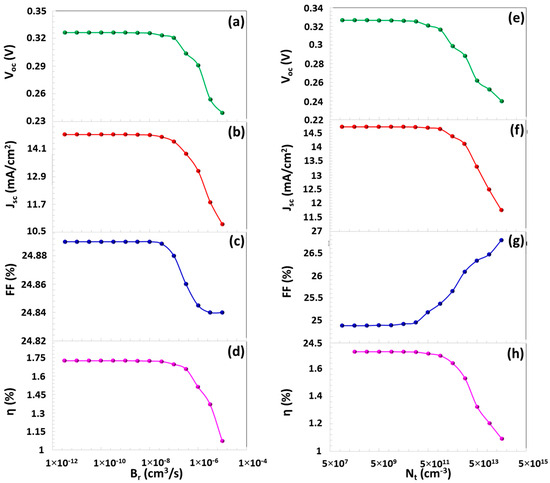
Figure 8.
Voc, Jsc, FF and η parameters depending on (a–d) Br and (e–h) Nt values.
3.4.2. The Effect of Defect Density (Nt) at the Interface of CZTS (C-II)/n-Si Heterojunction
Defect structures that can occur at the interface of heterojunction solar cells can cause the load carriers to recombine, resulting in a drop in PV performance [15]. In particular, factors such as the SiOx layer that can form on the surface of the Si wafer, sagging bonds, morphological disorders during CZTS thin film deposition, and the possibility of pinholes and cracks can cause defect formation at the interface of the CZTS/Si heterojunction. There was a decrease in the parameters (Jsc, Voc, η) after Nt = 1 × 1010 cm−3 in the change graph of PV parameters depending on the Nt interface defect density in Figure 8e–h. Voc = 0.240 mV, Jsc = 11.75 mA/cm2, FF = 26.79%, η = 1.09 for Nt = 5 × 1014 cm−3. The increase in Nt led to a significant decrease in the efficiency of the solar cell [35,36].
3.4.3. The Effect of Operating Temperature of Ag/CZTS (C-II) /n-Si/Al Heterojunction Solar Cell
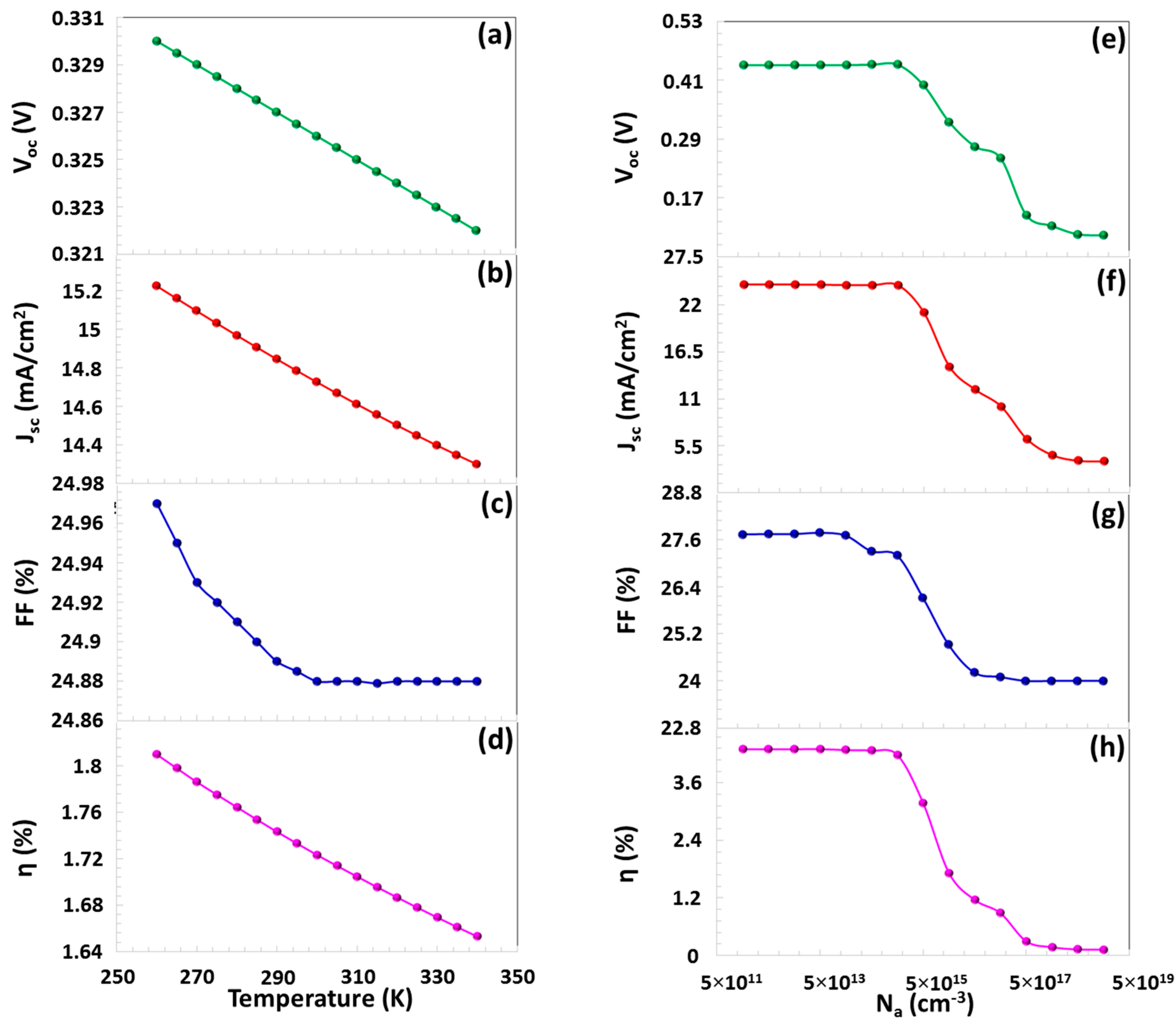
The temperature values of the environment where solar cells are accommodated have an effect on the operating performance of the solar cell. As the operating temperature augments, the kinetics of the charges in the semiconductor can enhance and exhibit unstable movements. This can cause current leakage and a higher in the saturated current. Additionally, the decline in the band gap of the semiconductor with the increase in temperature reduces the building voltage in the depletion region. This leads to a decrease in the electrical field in the depletion region and a weakening of charge separation, and thus there is a drop in the Voc value. The graph in Figure 9a–d shows that the PV parameters decrease linearly as the temperature rises from 260 K to 340 K. When the temperature reaches 260 K to 340 K, Voc, Jsc, FF and η that decreases from 0.330 mV to 0.322 mV, from 15.22 mA/cm2 to 14.30 mA/cm2, from 24.97% to 24.88% and from 1.80% to 1.65%, respectively. These results show that the solar cell is negatively affected by temperature and needs a cooling mechanism.
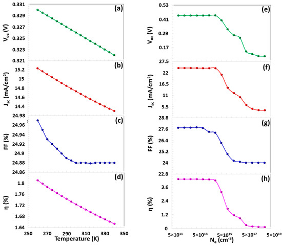
Figure 9.
Voc, Jsc, FF, and η parameters depending on (a–d) operating temperature and (e–h) Na values.
3.4.4. The Effect of the Shallow Acceptor Defect Density (Na) in CZTS (C-II) Ultrathin Film
The acceptor/donor defect density is a factor that determines the electrical conductivity of a semiconductor. The density of acceptor defects (Na) can cause the charge carriers to recombine. Especially, the increase in the Na value of a p-type CZTS semiconductor containing an electron minority charge carrier can cause more recombination for electrons. Therefore, CZTS thin film includes minority charge carriers whose lifetime is limited, meaning that the charge accumulation in solar cell decreases and the operating performance is negatively affected by this situation [37]. According to Figure 9e–h, there was no significant difference in the operating performance of the solar cell for values lower than Na = 5 × 1015 cm−3. As this Na value increases, so does the hole charge number increment. Therefore, the lifetime of the active layer is reduced and the solar cell efficiency decreases due to the recombination of the hole/electron charges within the CZTS ultrathin film. Here, the efficiency of the solar cell for Na = 5 × 1015 cm−3 has been verified. When the Na augments from 5 × 1015 cm−3 to 1 × 1019 cm−3, Voc, Jsc, FF and η decrease from 0.324 mV to 0.094 mV, from 14.73 mA/cm2 to 3.66 mA/cm2, from 25% to 24% and from 1.72% to 0.12%, respectively.
4. Conclusions
In this study, the PLD system was used to produce CZTS ultrathin films with 61 nm and 313 nm thicknesses. The crystalline sizes of C-I and C-II ultrathin films are 7.34 nm and 22.25 nm, and their band gaps are 1.95 eV and 1.45 eV, respectively. C-I and C-II thin films are Sn-rich and Cu-poor. Ag/CZTS (C-I, C-II)/n-Si/Al heterojunction solar cells were fabricated and the SCAPS-1D simulation program was employed to model these solar cells. The efficiency of the C-II solar cell is considerably higher than that of the C-I solar cell. The PV parameters calculated as a result of using the physical parameters of the semiconductors in the simulation program are in good agreement with the experimental parameters, which shows that the solar cells operate reliably. Jsc, Voc, FF, and η values of C-II solar cells (at highest efficiency) were calculated as a function of the radiative recombination coefficient, operating temperature, interface defect density, and acceptor defect density and thus the possible values of these parameters were determined.
Author Contributions
Conceptualization, S.Y.G. and H.S.K.; methodology, S.Y.G.; software, S.Y.G.; validation, S.Y.G., Y.G.K. and H.S.K.; formal analysis, S.Y.G. and H.S.K.; investigation, S.Y.G.; resources, S.Y.G. and Y.G.K.; data curation, S.Y.G.; writing—original draft preparation, S.Y.G. and Y.G.K.; writing—review and editing, S.Y.G., H.S.K. and Y.G.K.; visualization, S.Y.G. and Y.G.K.; supervision, S.Y.G. and H.S.K.; project administration, S.Y.G. and H.S.K. All authors have read and agreed to the published version of the manuscript.
Funding
This research received no external funding.
Institutional Review Board Statement
Not applicable.
Informed Consent Statement
Not applicable.
Data Availability Statement
The data are not publicly available.
Acknowledgments
Authors kindly would like to thank, Marc Burgelman’s group at The University of Gent, Belgium for offering SCAPS-1D simulation program and Selçuk University, High Technology Research and Application Center.
Conflicts of Interest
The authors declare no conflicts of interest.
Abbreviations
| Cu2ZnSnS4 | Copper Zinc Tin Sulfide. |
| CuInGaSe2 | Copper Indium Gallium Selenide. |
| CdTe | Cadmium Tellur. |
| CdS | Cadmium Sulfide. |
| I-ZnO | Intrinsic Zinc Oxide. |
| ITO | Indium–Tin Oxide. |
| SGSC | Second Generation Solar Cells. |
| Si | Silicon. |
| SCAPS-1D | One-dimensional Solar Cell Capacitance Simulator. |
| Jsc | Short-Circuit Current Density. |
| Voc | Open-Circuit Voltage. |
| FF | Fill Factor. |
| η | Power Conversion Efficiency. |
| Ag | Silver. |
| Al | Aluminum. |
| C-I | Copper Zinc Tin Sulfide -1. |
| C-II | Copper Zinc Tin Sulfide -2. |
| PLD | Pulse Laser Deposition. |
| SEM | Scanning Electron Microscope. |
| HR-TEM | High-Resolution Transmission Electron Microscopy. |
| XRD | X-ray Diffraction. |
| UVvis | Ultraviolet–visible. |
| eV | Electron Volt. |
| nm | Nanometer. |
| α | Absorption coefficient. |
| W | Thickness. |
| A | Absorbance. |
| Br | Radiative Recombination Coefficient. |
| PV | Photovoltaic. |
| Nt | Interface Defect Density. |
| K | Kelvin. |
| Na | Shallow Acceptor Defect Density. |
References
- Song, X.; Ji, X.; Li, M.; Lin, W.; Luo, X.; Zhang, H. A review on development prospect of CZTS based thin film solar cells. Int. J. Photoenergy 2014, 1, 613173. [Google Scholar] [CrossRef]
- Kişnişci, Z.; Özel, F.; Tuğluoğlu, N.; Yüksel, Ö.F. Structural and optical properties of Cu2ZnSnSe4 nanocrystals thin film. Opt. Quantum Electron. 2024, 56, 1239. [Google Scholar] [CrossRef]
- Kişnişci, Z.; Özel, F.; Karadeniz, S.; Tuğluoğlu, N.; Özel, S.S.; Yüksel, Ö.F. Electrical properties of Al/CZTSe nanocrystal Schottky diode. J. Mater. Sci. Mater. Electron. 2024, 35, 773. [Google Scholar] [CrossRef]
- Yeh, M.-Y.; Lei, P.-H.; Lin, S.-H.; Yang, C.-D. Copper-Zinc-Tin-Sulfur Thin Film Using Spin-Coating Technology. Materials 2016, 9, 526. [Google Scholar] [CrossRef]
- Tanaka, K.; Oonuki, M.; Moritake, N.; Uchiki, H. Cu2ZnSnS4 thin film solar cells prepared by non-vacuum processing. Sol. Energy Mater. Sol. Cells 2009, 93, 583–587. [Google Scholar] [CrossRef]
- Cui, H.; Liu, X.; Sun, L.; Liu, F.; Yan, C.; Hao, X. Fabrication of Efficient Cu2ZnSnS4 Solar Cells by Sputtering Single Stoichiometric Target. Coatings 2017, 7, 19. [Google Scholar] [CrossRef]
- Dalapati, G.K.; Zhuk, S.; Masudy-Panah, S.; Kushwaha, A.; Seng, H.L.; Chellappan, V.; Suresh, V.; Su, Z.; Batabyal, S.K.; Tan, C.C.; et al. Impact of molybdenum out diffusion and interface quality on the performance of sputter grown CZTS based solar cells. Sci. Rep. 2017, 7, 1350. [Google Scholar] [CrossRef] [PubMed]
- Singh, S.; Katiyar, A.K.; Midya, A.; Ghorai, A.; Ray, S.K. Superior heterojunction properties of solution processed copper-zinc-tin-sulphide quantum dots on Si. Nanotechnology 2017, 28, 435704. [Google Scholar] [CrossRef]
- Elhmaidi, Z.; Pandiyan, R.; Abd-Lefdil, M.; Saucedo, E.; El Khakani, M. In-situ tuning of the zinc content of pulsed-laser-deposited CZTS films and its effect on the photoconversion efficiency of p-CZTS/n-Si heterojunction photovoltaic devices. Appl. Surf. Sci. 2020, 507, 145003. [Google Scholar] [CrossRef]
- Oulad Elhmaidi, Z.; Abd-Lefdil, M.; El Khakani, M.A. Photoconversion Optimization of Pulsed-Laser-Deposited p-CZTS/n-Si-Nanowires Heterojunction-Based Photovoltaic Devices. Nanomaterials 2020, 10, 1393. [Google Scholar] [CrossRef]
- Yiğit gezgin, S.; Houimi, A.; Kiliç, H.Ş. Comparison of electrical and photovoltaic parameters of the hetero-junction solar cells based on CZTS and CIGS ultrathin films. Mater. Technol. 2022, 37, 1573–1585. [Google Scholar] [CrossRef]
- Song, N.; Young, M.; Liu, F.; Erslev, P.; Wilson, S.; Harvey, S.P.; Teeter, G.; Huang, Y.; Hao, X.; Green, M.A. Epitaxial Cu2ZnSnS4 thin film on Si (111) 4 substrate. Appl. Phys. Lett. 2015, 106, 252102. [Google Scholar] [CrossRef]
- Song, N.; Green, M.A.; Sun, K.; Hu, Y.; Yan, C.; Hao, X. Epitaxial Growth of Cu2ZnSnS4 Thin Films. Appl. Phys. Lett. 2020, 116, 123901. [Google Scholar] [CrossRef]
- Yiğit Gezgin, S.; Kiliç, H.Ş. The effect of Ag plasmonic nanoparticles on the efficiency of CZTS solar cell: An experimental investigation and numerical modelling. Indian J. Phys. 2023, 97, 779–796. [Google Scholar] [CrossRef]
- Gezgin, S.Y. Modelling and investigation of the electrical properties of CIGS/n-Si heterojunction solar cells. Opt. Mater. 2022, 131, 112738. [Google Scholar] [CrossRef]
- Houimi, A.; Gezgin, S.Y.; Mercimek, B.; Kılıç, H.Ş. Numerical analysis of CZTS/n-Si solar cells using SCAPS-1D. A comparative study between experimental and calculated outputs. Opt. Mater. 2021, 121, 111544. [Google Scholar] [CrossRef]
- Cazzaniga, A.C. Fabrication of Thin Film CZTS Solar Cells with Pulsed Laser Deposition. Ph.D. Thesis, Technical University of Denmark (DTU), Kongens Lyngby, Denmark, 2016. [Google Scholar]
- Dikovska, A.O.; Atanasov, P.A.; Vasileva, C.; Dimitrov, I.G.; Stoyanchov, T.R. Thin ZnO films produced by pulsed laser deposition. J. Optoelectron. Adv. Mater. 2005, 7, 1329–1334. [Google Scholar]
- Ghimbeu, C.M.; Sima, F.; Ostaci, R.; Socol, G.; Mihailescu, I.; Vix-Guterl, C. Crystalline vanadium nitride ultra-thin films obtained at room temperature by pulsed laser deposition. Surf. Coat. Technol. 2012, 211, 158–162. [Google Scholar] [CrossRef]
- Gezgin, S.Y.; Kepceoğlu, A.; Kılıç, H.Ş. An investigation of localised surface plasmon resonance (LSPR) of Ag nanoparticles produced by pulsed laser deposition (PLD) technique. AIP Conf. Proc. 2017, 1815, 030019. [Google Scholar] [CrossRef]
- Camara, S.M.; Wang, L.; Zhang, X. Easy hydrothermal preparation of Cu2ZnSnS4 (CZTS) nanoparticles for solar cell application. Nanotechnology 2013, 24, 495401. [Google Scholar] [CrossRef]
- Gezgin, S.Y.; Kiliç, H.Ş. The Electrical Characteristics of ITO/CZTS/ZnO/Al and ITO/ZnO/CZTS/Al Heterojunction Diodes. Optik 2019, 182, 356–371. [Google Scholar] [CrossRef]
- Tao, J.; Zhang, K.; Zhang, C.; Chen, L.; Cao, H.; Liu, J.; Jiang, J.; Sun, L.; Yang, P.; Chu, J. A sputtered CdS buffer layer for co-electrodeposited Cu 2 ZnSnS 4 solar cells with 6.6% efficiency. Chem. Commun. 2015, 51, 10337–10340. [Google Scholar] [CrossRef]
- Wang, J.; Zeng, X.; Zhao, Y.; Zhang, W. Preparation and photocatalytic properties of Cu2ZnSnS4 for H2 production. Mater. Res. Express 2020, 7, 095902. [Google Scholar] [CrossRef]
- Đekić, M.; Fetic, A.S. Influence of deposition parameters on pulsed laser deposition of K0.3MoO3 thin films. Bull. Chem. Technol. Bosnia Herzeg. 2017, 48, 1. [Google Scholar]
- Vakulov, Z.; Ivonin, M.; Zamburg, E.G.; Klimin, V.S.; Volik, D.P.; A Golosov, D.; Zavadskiy, S.M.; Dostanko, A.P.; Miakonkikh, A.V.; E Clemente, I.; et al. Size effects in LiNbO3 thin films fabricated by pulsed laser deposition. J. Phys. Conf. Ser. 2018, 1124, 022032. [Google Scholar] [CrossRef]
- Cazzaniga, A.; Crovetto, A.; Yan, C.; Sun, K.; Hao, X.; Estelrich, J.R.; Canulescu, S.; Stamate, E.; Pryds, N.; Hansen, O.; et al. Ultra-thin Cu2ZnSnS4 solar cell by pulsed laser deposition. Sol. Energy Mater. Sol. Cells 2017, 166, 91–99. [Google Scholar] [CrossRef]
- Kim, C.; Hong, S. Optical and electrical properties of Cu2ZnSnS4 thin films grown using spray pyrolysis technique and annealing in air. Mol. Cryst. Liq. Cryst. 2017, 645, 217–224. [Google Scholar] [CrossRef]
- Gupta, G.K.; Reddy, V.; Dixit, A. Impact of excess and disordered Sn sites on Cu2ZnSnS4 absorber material and device performance: A 119Sn Mössbauer study. Mater. Chem. Phys. 2019, 225, 410–416. [Google Scholar] [CrossRef]
- Mustafa, F.A. Optical properties of NaI doped polyvinyl alcohol films. Phys. Sci. Res. Int. 2013, 1, 1–9. [Google Scholar] [CrossRef]
- Antar, E. Effect of γ-ray on optical characteristics of dyed PVA films. J. Radiat. Res. Appl. Sci. 2014, 7, 129–134. [Google Scholar] [CrossRef]
- Akın, Ü.; Houimi, A.; Gezgin, B.; Gündoğdu, Y.; Kılıç, S.; Mercimek, B.; Berber, A.; Gezgin, S.Y. The electrical properties of ZnO/Si heterojunction diode depending on thin film thickness. J. Korean Phys. Soc. 2022, 81, 139–149. [Google Scholar] [CrossRef]
- Adewoyin, A.D.; Olopade, M.A.; Chendo, M. Enhancement of the conversion efficiency of Cu2ZnSnS4 thin film solar cell through the optimization of some device parameters. Optik 2017, 133, 122–131. [Google Scholar] [CrossRef]
- He, Y.; Chen, H.; Wang, S.; Wang, Q.; Zhang, C.; Hao, Q.; Li, R.; Li, S.; Liu, X.; Guo, X. Unveiling recombination in top cells: SCAPS-1D simulations for high-efficiency bifacial planar perovskite/silicon tandem solar cells. Sol. Energy 2024, 282, 112921. [Google Scholar] [CrossRef]
- Peksu, E.; Karaagac, H. A third generation solar cell based on wet-chemically etched Si nanowires and sol-gel derived Cu2ZnSnS4 thin films. J. Alloys Compd. 2019, 774, 1117–1122. [Google Scholar] [CrossRef]
- Gupta, G.K.; Dixit, A. Simulation studies of CZT (S, Se) single and tandem junction solar cells towards possibilities for higher efficiencies up to 22%. arXiv 2018, arXiv:1801.08498. [Google Scholar] [CrossRef]
- Meher, S.; Balakrishnan, L.; Alex, Z. Analysis of Cu2ZnSnS4/CdS based photovoltaic cell: A numerical simulation approach. Superlattices Microstruct. 2016, 100, 703–722. [Google Scholar] [CrossRef]
Disclaimer/Publisher’s Note: The statements, opinions and data contained in all publications are solely those of the individual author(s) and contributor(s) and not of MDPI and/or the editor(s). MDPI and/or the editor(s) disclaim responsibility for any injury to people or property resulting from any ideas, methods, instructions or products referred to in the content. |
© 2025 by the authors. Licensee MDPI, Basel, Switzerland. This article is an open access article distributed under the terms and conditions of the Creative Commons Attribution (CC BY) license (https://creativecommons.org/licenses/by/4.0/).

