
Theoretical Analysis of Power Conversion Efficiency of Lead-Free Double-Perovskite Cs2TiBr6 Solar Cells with Different Hole Transport Layers


Abstract
1. Introduction
- Stability: Photovoltaic technologies need to meet the stability and durability standards laid out by IEC 61646 testing procedures if they are to be economically viable. Particularly for thin-film solar goods, these criteria are crucial. Hysteresis causes perovskite films to undergo metastable transformation, which drastically lowers their initial PCE. Even with consistent light intensity and temperature, this decrease can reach 50% in the first 10 h under short-circuit settings and 20% under open-circuit conditions [18].
- Toxicity: Solar cells have a long way to go before they can be mass produced due to concerns about lead poisoning, stability, and the absence of an efficient manufacturing process. There has been extensive research on the impact of lead (and tin) toxicity on human health and its dynamics. This finding has sparked significant concerns, especially about the various mechanisms through which contamination might happen. One specific area of concentration has been the impact of rainfall on PSC modules. Increased concentrations of lead can contribute to the onset of anemia, muscle weakness, as well as harmful impacts on the kidneys and brain. High levels of lead exposure can lead to mortality. Lead may traverse the placental barrier; hence, pregnant women who come into contact with lead are also subjecting their unborn child to it. Lead can have deleterious effects on the developing neurological system of an infant. Chronic lead exposure increases the risk of hypertension, cardiovascular disease, kidney disease, and reduced fertility in humans.
2. Materials and Methods
3. Results
4. Conclusions
Author Contributions
Funding
Informed Consent Statement
Data Availability Statement
Acknowledgments
Conflicts of Interest
References
- Jordehi, A.R. Parameter estimation of solar photovoltaic (PV) cells: A review. Renew. Sustain. Energy Rev. 2016, 61, 354–371. [Google Scholar] [CrossRef]
- Kalogirou, S.A. Introduction to Renewable Energy Powered Desalination. In Renewable Energy Powered Desalination Handbook Application and Thermodynamics; Butterworth-Heinemann: Oxford, UK, 2018; pp. 3–46. [Google Scholar] [CrossRef]
- PVPS. Snapshot of Global Photovoltaic Markets: 2015; Report IEA PVPS T1-29; PVPS, 2016. [Google Scholar]
- Ji, L. Metal oxide-based thermoelectric materials. In Metal Oxides in Energy Technologies; Wu, Y., Ed.; Elsevier: Amsterdam, The Netherlands, 2018; pp. 49–72. ISBN 9780128111673. [Google Scholar]
- Masood, M.T. Solution-Processable Compact and Mesoporous Titanium Dioxide Thin Films as Electron-Selective Layers for Perovskite Solar Cells. Ph.D. Thesis, Ǻbo Akademi University, Turku, Finland, 2020. [Google Scholar]
- Eperon, G.E. Inorganic caesium lead iodide perovskite solar cells. J. Mater. Chem. A 2015, 3, 19688–19695. [Google Scholar] [CrossRef]
- Kim, H.S.; Lee, C.R.; Im, J.H.; Lee, K.B.; Moehl, T.; Marchioro, A.; Moon, S.J.; Humphry-Baker, R.; Yum, J.H.; Moser, J.E.; et al. Lead iodide perovskite sensitized all-solid-state submicron thin film mesoscopic solar cell with efficiency exceeding 9%. Sci. Rep. 2012, 2, 591. [Google Scholar] [CrossRef]
- Icli, K.C.; Ozenbas, M. Fully metal oxide charge selective layers for n-i-p perovskite solar cells employing nickel oxide nanoparticles. Electrochim. Acta 2018, 263, 338–345. [Google Scholar] [CrossRef]
- Ye, J.; Zheng, H.; Zhu, L.; Liu, G.; Zhang, X.; Hayat, T.; Pan, X.; Dai, S. Enhanced Moisture Stability of Perovskite Solar Cells With Mixe Dimensional and Mixed-Compositional Light-Absorbing Materials. Solar RRL 2017, 1, 1700125. [Google Scholar] [CrossRef]
- El Cohen, B.; Wierzbowska, M.; Etgar, L. High Efficiency and High Open Circuit Voltage in Quasi 2D Perovskite Based Solar Cells. Adv. Funct. Mater. 2017, 27, 1604733. [Google Scholar] [CrossRef]
- Koh, T.M.; Shanmugam, V.; Schlipf, J.; Oesinghaus, L.; Müller-Buschbaum, P.; Ramakrishnan, N.; Swamy, V.; Mathews, N.; Boix, P.P.; Mhaisalkar, S.G. Nanostructuring Mixed-Dimensional Perovskites: A Route Toward Tunable, Efficient Photovoltaics. Adv. Mater. 2016, 28, 3653–3661. [Google Scholar] [CrossRef]
- Sidhik, S.; Esparza, D.; Martínez-Benítez, A.; López-Luke, T.; Carriles, R.; De la Rosa, E. Improved performance of mesoscopic perovskite solar cell using an accelerated crystalline formation method. J. Power Sources 2017, 365, 169–178. [Google Scholar] [CrossRef]
- Wang, P.; Zhang, X.; Zhou, Y.; Jiang, Q.; Ye, Q.; Chu, Z.; Li, X.; Yang, X.; Yin, Z.; You, J. Solvent-controlled growth of inorganic perovskite films in dry environment for efficient and stable solar cells. Nat. Commun. 2018, 9, 2225. [Google Scholar] [CrossRef]
- Mali, S.S.; Kim, H.; Kim, H.H.; Shim, S.E.; Hong, C.K. Nanoporous p-type NiOx electrode for p-i-n inverted perovskite solar cell toward air stability. Mater. Today 2018, 21, 483–500. [Google Scholar] [CrossRef]
- Wang, Z.Y.; Lee, S.H.; Kim, D.H.; Kim, J.H.; Park, J.G. Effect of NiOx thin layer fabricated by oxygen-plasma treatment on polymer photovoltaic cell. Sol. Energy Mater. Sol. Cells 2010, 94, 1591–1596. [Google Scholar] [CrossRef]
- Lin, Z.; Chang, J.; Zhu, H.; Xu, Q.H.; Zhang, C.; Ouyang, J.; Hao, Y. Enhanced planar heterojunction perovskite solar cell performance and stability using PDDA polyelectrolyte capping agent. Sol. Energy Mater. Sol. Cells 2017, 172, 133–139. [Google Scholar] [CrossRef]
- Zhao, D.; Sexton, M.; Park, H.Y.; Baure, G.; Nino, J.C.; So, F. High-efficiency solution-processed planar perovskite solar cells with a polymer hole transport layer. Adv. Energy Mater. 2015, 5, 1401855. [Google Scholar] [CrossRef]
- Lu, J.; Jiang, L.; Li, W.; Li, F.; Pai, N.K.; Scully, A.D.; Tsai, C.M.; Bach, U.; Simonov, A.N.; Cheng, Y.B.; et al. Diammonium and Monoammonium Mixed-Organic-Cation Perovskites for High Performance Solar Cells with Improved Stability. Adv. Energy Mater. 2017, 7, 1700444. [Google Scholar] [CrossRef]
- Kumar, N.; Rani, J.; Kurchania, R. A review on power conversion efficiency of lead iodide perovskite-based solar cells. Mater. Today Proc. 2020, 46, 5570–5574. [Google Scholar] [CrossRef]
- Sun, K.; Li, P.; Xia, Y.; Chang, J.; Ouyang, J. Transparent Conductive Oxide-Free Perovskite Solar Cells with PEDOT:PSS as Transparent Electrode. ACS Appl. Mater. Interfaces 2015, 7, 15314–15320. [Google Scholar] [CrossRef]
- Ye, S.; Sun, W.; Li, Y.; Yan, W.; Peng, H.; Bian, Z.; Liu, Z.; Huang, C. CuSCN-Based Inverted Planar Perovskite Solar Cell with an Average PCE of 15.6%. Nano Lett. 2015, 15, 3723–3728. [Google Scholar] [CrossRef]
- Wang, J.; Ye, X.; Wang, Y.; Wang, Z.; Wong, W.; Li, C. Halide perovskite based on hydrophobic ionic liquid for stability improving and its application in high-efficient photovoltaic cell. Electrochim. Acta 2019, 303, 133–139. [Google Scholar] [CrossRef]
- Zhao, X.G.; Yang, D.N.; Ren, J.; Sun, Y.; Xiao, Z. Rational Design of Halide Double Perovskites for Optoelectronic Applications. Joule 2018, 2, 1662–1673. [Google Scholar] [CrossRef]
- Giorgi, G.; Yamashita, K. Organic-Inorganic halide perovskites: An ambipolar class of materials with enhanced photovoltaic performances. J. Mater. Chem. A 2014, 3, 8981–8991. [Google Scholar] [CrossRef]
- Kim, Y.G.; Kim, T.Y.; Oh, J.H.; Choi, K.S.; Kim, Y.J.; Kim, S.Y. Cesium lead iodide solar cells controlled by annealing temperature. Phys. Chem. Chem. Phys. 2017, 19, 6257–6263. [Google Scholar] [CrossRef] [PubMed]
- Sanehira, E.M.; Marshall, A.R.; Christians, J.A.; Harvey, S.P.; Ciesielski, P.N.; Wheeler, L.M.; Schulz, P.; Lin, L.Y.; Beard, M.C.; Luther, J.M. Enhanced mobility CsPbI3 quantum dot arrays for record-efficiency, high-voltage photovoltaic cells. Sci. Adv. 2017, 3, eaao4204. [Google Scholar] [CrossRef] [PubMed]
- Jonathan, L.; Diguna, L.J.; Samy, O.; Muqoyyanah, M.; AbuBakar, S.; Birowosuto, M.D.; El Moutaouakil, A. Hybrid Organic Inorganic Perovskite Halide Materials for Photovoltaics towards Their Commercialization. Polymers 2022, 14, 2073–4360. [Google Scholar] [CrossRef] [PubMed]
- Wang, Z.; Lin, Q.; Chmiel, F.P.; Sakai, N.; Herz, L.M.; Snaith, H.J. Efficient ambient-air-stable solar cells with 2D-3D heterostructuredbutylammonium-caesium-formamidinium lead halide perovskites. Nat. Energy 2017, 2, 17135. [Google Scholar] [CrossRef]
- Zhou, Y.; Zhao, Y. Chemical stability and instability of inorganic halide perovskites. Energy Environ. Sci. 2019, 12, 1495–1511. [Google Scholar] [CrossRef]
- Euvrard, J.; Wang, X.; Li, T.; Yan, Y. Is Cs 2 TiBr 6 a promising Pb-free perovskite for solar energy applications? J. Mater. Chem. 2020, 8, 4049–4054. [Google Scholar] [CrossRef]
- Chen, M.; Ju, M.G.; Carl, A.D.; Zong, Y.; Grimm, R.L.; Gu, J.; Zeng, X.C.; Zhou, Y.; Padture, N.P. Cesium Titanium(IV) Bromide Thin Films Based Stable Lead-free Perovskite Solar Cells. Joule 2018, 2, 558–570. [Google Scholar] [CrossRef]
- Masood, M.T.; Weinberger, C.; Sarfraz, J.; Rosqvist, E.; Sandén, S.; Sandberg, O.J.; Vivo, P.; Hashmi, G.; Lund, P.D.; Osterbacka, R.; et al. Impact of film thickness of ultrathin dip-coated compact TiO2 layers on the performance of mesoscopic perovskite solar cells. ACS Appl. Mater. Interfaces 2017, 9, 17906–17913. [Google Scholar] [CrossRef]
- Bhojak, V.; Bhatia, D.; Jain, P.K.; Dargar, S.K.; Jasinski, M.; Gono, R.; Leonowicz, Z. Numerical Investigation of Power Conversion Efficiency of Sustainable Perovskite Solar Cells. Electronics 2023, 12, 1762. [Google Scholar] [CrossRef]
- Konidakis, I.; Karagiannaki, A.; Stratakis, E. Advanced composite glasses with metallic, perovskite, and two-dimensional nanocrystals for optoelectronic and photonic applications, The Royal Society of Chemistry. Nanoscale 2022, 14, 2966–2989. [Google Scholar] [CrossRef]
- Jani, M.; Islam, M.T.; Amin, S.A.; Sami, M. Exploring solar cell performance of inorganic Cs2TiBr6 halide double perovskite: A numerical study. Superlattices Microstruct. 2020, 146, 106652. [Google Scholar] [CrossRef]
- Available online: https://marc-burgelman-scaps.software.informer.com/ (accessed on 1 December 2024).
- He, Y.; Zheng, H.; Huang, S.; Liu, C.; Jiang, T.; Guo, X. Defect Investigation of Ti-Based Vacancy-Ordered Double Perovskite Solar Cell using SCAPS-1D. J. Phys. Conf. Ser. 29 Oct 2021, 2044, 012100. [Google Scholar] [CrossRef]
- Ahmed, S.; Jannat, F.; Khan, M.K.; Alim, M.A. Numerical development of eco-friendly Cs2TiBr6 based perovskite solar cell with all-inorganic charge transport materials via SCAPS-1D. Opt. Int. J. Light Electron Opt. 2021, 225, 165765. [Google Scholar] [CrossRef]
- Syed, A.; Moiz, S.A. Optimization of Hole and Electron Transport Layer for Highly Efficient Lead-Free Cs2TiBr6-Based Perovskite Solar Cell. Photonics 2021, 9, 23. [Google Scholar] [CrossRef]
- Serpetzoglou, E.; Konidakis, I.; Maksudov, T.; Panagiotopoulos, A.; Kymakis, E.; Stratakis, E. In situ monitoring of the charge carrier dynamics of CH3NH3PbI3 perovskite crystallization process. J. Mater. Chem. C 2019, 7, 12170–12179. [Google Scholar] [CrossRef]
- Serpetzoglou, E.; Konidakis, I.; Kourmoulakis, G.; Demeridou, I.; Chatzimanolis, K.; Zervos, C.; Kioseoglou, G.; Kymakis, E.; Stratakis, E. Charge carrier dynamics in different crystal phases of CH3NH3PbI3 perovskite. Opto-Electron. Sci. 2022, 1, 210005. [Google Scholar] [CrossRef]
- Zhang, M.; Ma, X.; Zhang, H.; Zhu, L.; Xu, W.; Sun, S.; Jeong, S.Y.; Woo, H.Y.; Zhang, J.; Zhang, F. Over 19.1% efficiency for sequentially spin-coated polymer solar cells by employing ternary strategy. Chem. Eng. J. 2023, 471, 144711. [Google Scholar]
- Zhou, H.; Sun, Y.; Zhang, M.; Ni, Y.; Zhang, F.; Jeong, S.Y.; Huang, T.; Li, X.; Woo, H.Y.; Zhang, J.; et al. Over 18.2% efficiency of layer–by–layer all–polymer solar cells enabled by homoleptic iridium(III) carbene complex as solid additive. Sci. Bull. 2024, 69, 2862–2869. [Google Scholar] [CrossRef]
- Zhang, L.; Zhang, M.; Ni, Y.; Xu, W.; Zhou, H.; Ke, S.; Tian, H.; Jeong, S.Y.; Woo, H.Y.; Wong, W.Y.; et al. Over 17.1% or 18.2% Efficiency of Layer-by-Layer All-Polymer Solar Cells via Incorporating Efficient Pt Complexes as Energy Donor Additive. ACS Mater. Lett. 2024, 6, 2964–2973. [Google Scholar] [CrossRef]
- Karimi, E.; Ghorashi, S.M.B. Investigation of the influence of different hole-transporting materials on the performance of perovskite solar cells. Optik 2017, 130, 650–658. [Google Scholar] [CrossRef]


| Material Properties | Cs2TiBr6 | C60 | Cu2O | CuI | FTO |
|---|---|---|---|---|---|
| Layer thickness (µm) | 0.2 to 2 | 0.14 | 0.15 | 0.05 | 500 |
| Optical bandgap (eV) | 1.8 | 1.7 | 2.17 | 3.1 | 3.5 |
| Affinity of electron (eV) | 4.0 | 3.9 | 3.2 | 2.1 | 4 |
| Relative permittivity | 10 | 4.2 | 7.11 | 6.5 | 9 |
| Effective DOS in the conduction band (cm−3) | 6 × 10¹⁸ | 8 × 10¹⁹ | 2.2 × 10¹⁸ | 2.2 × 10¹⁸ | 2.2 × 10¹⁸ |
| Effective DOS in the valance band (cm−3) | 2.14 × 10¹⁸ | 8 × 10¹⁹ | 1.9 × 10¹⁹ | 1.8 × 10¹⁹ | 1.8 × 10¹⁹ |
| Thermal velocity of electron (cm/s) | 107 | 107 | 107 | 107 | 107 |
| Thermal velocity of hole (cm/s) | 107 | 107 | 107 | 107 | 107 |
| Mobility of electron (cm2/Vs) | 2.36 × 101 | 1 × 10⁻² | 3 × 10² | 100 | 20 |
| Hole mobility (cm2/Vs) | 1.71 × 101 | 3.5 × 10⁻³ | 8 × 101 | 47.9 | 10 |
| Donor density (cm−3) | −3 × 10¹⁹ | 2.6 × 10¹⁸ | - | - | 1 × 10¹⁹ |
| Acceptor density (cm−3) | 3 × 10¹⁸ | - | 1 × 10¹⁸ | 1 × 10¹⁸ | - |
| Defect density (1/cm3) | 1014 | 1014 | 1014 | 1014 | 1014 |
| Reference | [37] | [33] | [33] | [33] | [33] |
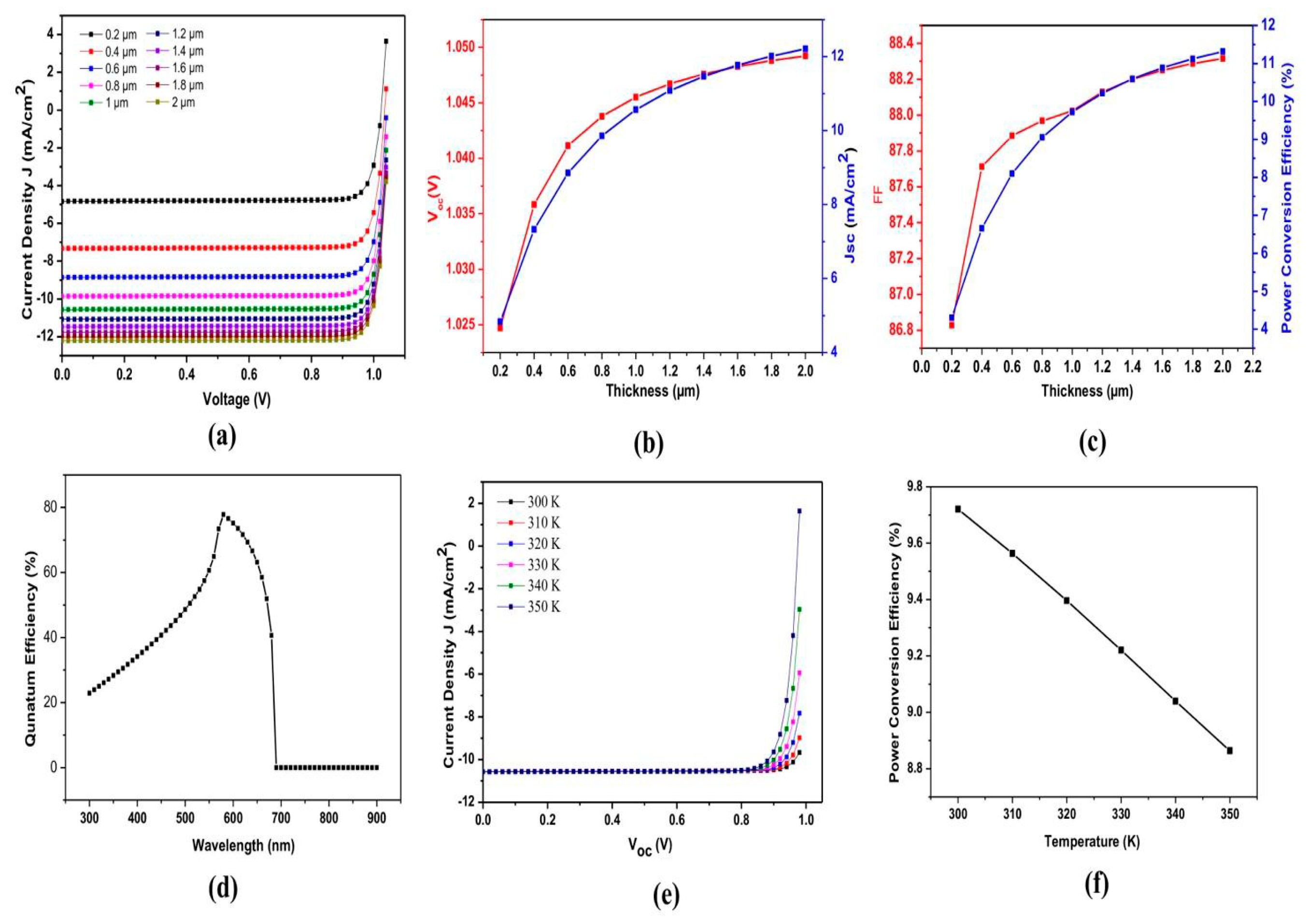
| Thickness (µm) | Voc | Jsc | FF | Efficiency (%) |
|---|---|---|---|---|
| 0.2 | 1.02 | 4.83 | 86.82 | 4.30 |
| 0.4 | 1.03 | 7.32 | 87.71 | 6.65 |
| 0.6 | 1.04 | 8.85 | 87.88 | 8.10 |
| 0.8 | 1.04 | 9.86 | 87.96 | 9.05 |
| 1 | 1.04 | 10.56 | 88.02 | 9.72 |
| 1.2 | 1.04 | 11.07 | 88.12 | 10.21 |
| 1.4 | 1.04 | 11.46 | 88.20 | 10.59 |
| 1.6 | 1.04 | 11.76 | 87.2 | 10.88 |
| 1.8 | 1.04 | 12.01 | 87.28 | 11.12 |
| 2 | 1.04 | 12.20 | 88.31 | 11.31 |
| Temperature (K) | Voc | Jsc | FF | Efficiency (%) |
|---|---|---|---|---|
| 300 | 1.04 | 10.56 | 88.02 | 9.72 |
| 310 | 1.03 | 10.56 | 87.75 | 9.56 |
| 320 | 1.01 | 10.56 | 87.35 | 9.39 |
| 330 | 1.00 | 10.56 | 86.92 | 9.22 |
| 340 | 0.98 | 10.56 | 86.44 | 9.03 |
| 350 | 0.97 | 10.57 | 85.97 | 8.86 |
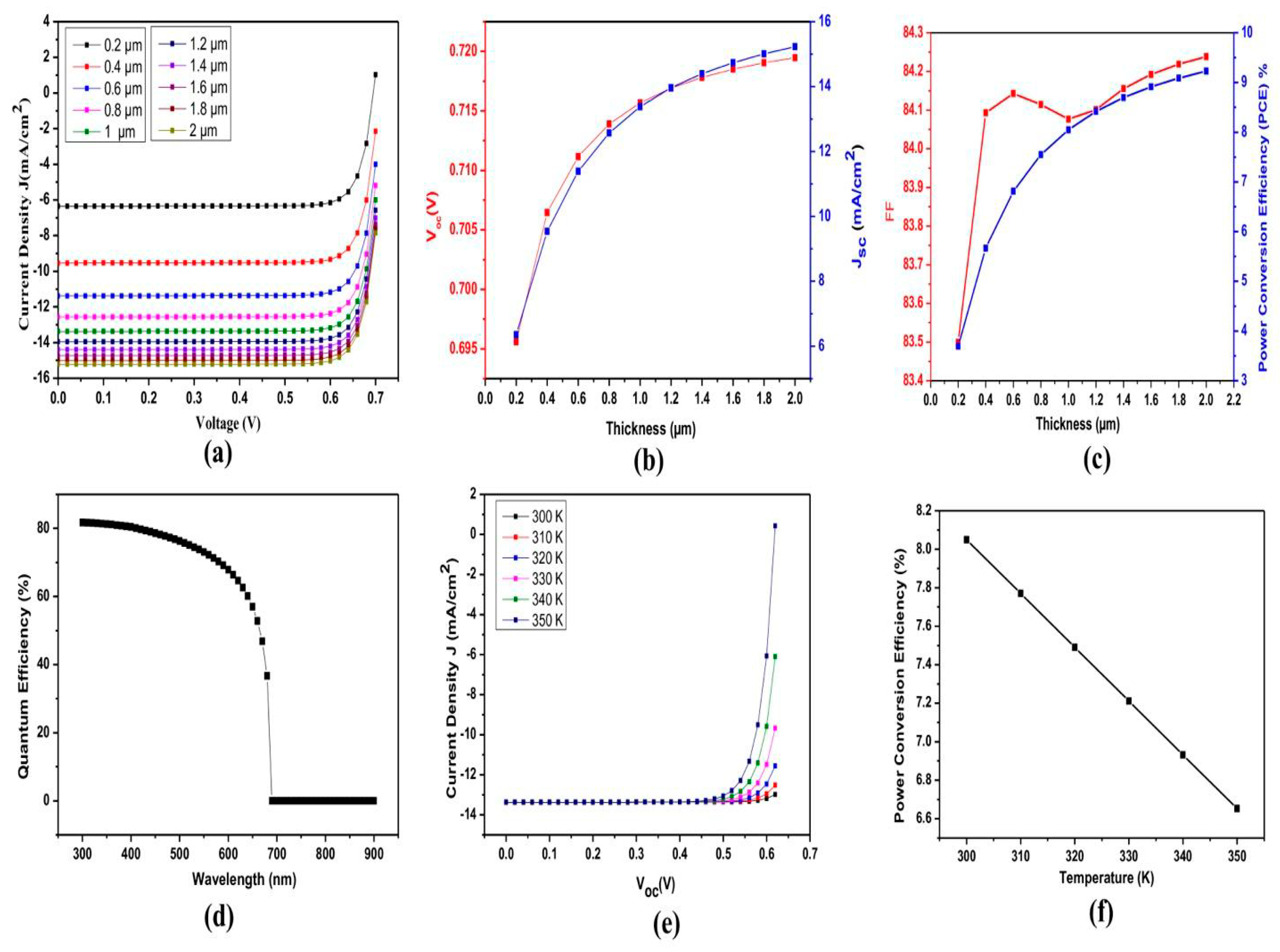
| Temperature (K) | Voc | Jsc | FF | Efficiency (%) |
|---|---|---|---|---|
| 300 | 0.71 | 13.37 | 84.07 | 8.04 |
| 310 | 0.69 | 13.37 | 83.38 | 7.77 |
| 320 | 0.67 | 13.37 | 82.67 | 7.49 |
| 330 | 0.65 | 13.37 | 81.96 | 7.21 |
| 340 | 0.63 | 13.37 | 81.15 | 6.93 |
| 350 | 0.61 | 13.37 | 80.34 | 6.65 |
| Thickness (µm) | Voc | Jsc | FF | Efficiency (%) |
|---|---|---|---|---|
| 0.2 | 0.69 | 6.35 | 83.49 | 3.69 |
| 0.4 | 0.70 | 9.53 | 84.09 | 5.66 |
| 0.6 | 0.71 | 11.38 | 84.14 | 6.81 |
| 0.8 | 0.71 | 12.56 | 84.11 | 7.54 |
| 1 | 0.71 | 13.37 | 84.07 | 8.04 |
| 1.2 | 0.71 | 13.96 | 84.10 | 8.41 |
| 1.4 | 0.71 | 14.39 | 84.15 | 8.69 |
| 1.6 | 0.71 | 14.73 | 84.19 | 8.91 |
| 1.8 | 0.71 | 15.00 | 84.21 | 9.08 |
| 2 | 0.71 | 15.22 | 84.23 | 9.22 |
| Defect Density (1/cm3) | Voc | Jsc | FF | Efficiency (%) |
|---|---|---|---|---|
| 1 × 10¹¹ | 1.04 | 10.57 | 88.06 | 9.73 |
| 1 × 10¹² | 1.04 | 10.57 | 88.06 | 9.73 |
| 1 × 10¹³ | 1.04 | 10.57 | 88.06 | 9.73 |
| 1 × 10¹⁴ | 1.04 | 10.56 | 88.02 | 9.72 |
| 1 × 10¹⁵ | 1.04 | 10.47 | 87.99 | 9.63 |
| 1 × 10¹⁶ | 1.04 | 9.70 | 87.86 | 8.89 |
| Defect Density (1/cm3) | Voc | Jsc | FF | Efficiency (%) |
|---|---|---|---|---|
| 1 × 10¹¹ | 0.71 | 13.39 | 84.07 | 8.05 |
| 1 × 10¹² | 0.71 | 13.39 | 84.07 | 8.05 |
| 1 × 10¹³ | 0.71 | 13.38 | 84.07 | 8.05 |
| 1 × 10¹⁴ | 0.71 | 13.37 | 84.07 | 8.04 |
| 1 × 10¹⁵ | 0.71 | 13.26 | 84.08 | 7.97 |
| 1 × 10¹⁶ | 0.71 | 12.31 | 84.11 | 7.38 |
| Structure | VOC | JSC | FF | PCE (%) | Parameters Optimized |
|---|---|---|---|---|---|
| C60/Cs2TiBr6/Cu2O (Proposed) [Thickness at 2 µm] | 1.04 | 12.20 | 88.31 | 11.31 | ETL, HTL, thickness of absorbing layer, defect density |
| C60/LMNO/Cu2O [33] | 0.19 | 1.92 | 49.5 | 0.43 | ETL, HTL, thickness of absorbing layer, defect density |
Disclaimer/Publisher’s Note: The statements, opinions and data contained in all publications are solely those of the individual author(s) and contributor(s) and not of MDPI and/or the editor(s). MDPI and/or the editor(s) disclaim responsibility for any injury to people or property resulting from any ideas, methods, instructions or products referred to in the content. |
© 2025 by the authors. Licensee MDPI, Basel, Switzerland. This article is an open access article distributed under the terms and conditions of the Creative Commons Attribution (CC BY) license (https://creativecommons.org/licenses/by/4.0/).
Share and Cite
Bhojak, V.; Jain, P.K. Theoretical Analysis of Power Conversion Efficiency of Lead-Free Double-Perovskite Cs2TiBr6 Solar Cells with Different Hole Transport Layers. Eng 2025, 6, 28. https://doi.org/10.3390/eng6020028
Bhojak V, Jain PK. Theoretical Analysis of Power Conversion Efficiency of Lead-Free Double-Perovskite Cs2TiBr6 Solar Cells with Different Hole Transport Layers. Eng. 2025; 6(2):28. https://doi.org/10.3390/eng6020028
Chicago/Turabian StyleBhojak, Vivek, and Praveen Kumar Jain. 2025. "Theoretical Analysis of Power Conversion Efficiency of Lead-Free Double-Perovskite Cs2TiBr6 Solar Cells with Different Hole Transport Layers" Eng 6, no. 2: 28. https://doi.org/10.3390/eng6020028
APA StyleBhojak, V., & Jain, P. K. (2025). Theoretical Analysis of Power Conversion Efficiency of Lead-Free Double-Perovskite Cs2TiBr6 Solar Cells with Different Hole Transport Layers. Eng, 6(2), 28. https://doi.org/10.3390/eng6020028