Article

A New Transformer-Less Structure for a Boost DC-DC Converter with Suitable Voltage Stress

by
Farzad Mohammadzadeh Shahir
,
Meysam Gheisarnejad
* and
Mohammad-Hassan Khooban
Department of Electrical and Computer Engineering, Aarhus University, 8200 Aarhus, Denmark
*
Author to whom correspondence should be addressed.
Automation 2021, 2(4), 220-237; https://doi.org/10.3390/automation2040014
Submission received: 14 August 2021 / Revised: 31 August 2021 / Accepted: 2 September 2021 / Published: 11 October 2021

Abstract

:
In this paper, a new structure is proposed for a boost dc–dc converter based on the voltage-lift (VL) technique. The main advantages of the proposed converter are its lack of transformer, simple structure, free and low input current ripple, high voltage gain capability by using an input source, suitable voltage stress on semiconductors and lower output capacitance. Herein, the analysis of the proposed converter operating and its elements voltage and current relations in continuous conduction mode (CCM) and discontinuous conduction mode (DCM) are presented, and the voltage gain of each operating mode is individually calculated. Additionally, the critical inductance, current stress of switches, calculation of passive components’ values and efficiency are analyzed. In addition, the proposed converter is compared with other studied boost converters in terms of ideal voltage gain in the CCM and the number of active and passive components, maximum voltage stress on semiconductors, and situation of input current ripples. The correctness of the theoretical concepts is examined from the experimental results using the laboratory prototype.

1. Introduction

The reduction of fossil fuels, increasing energy demands and increasing air pollution has created demand for energy production in the field of renewable energies such as wind turbines, solar cells and fuel cells. The structure of this kind of energy produces low level dc voltage at output, therefore, dc–dc converters are used in the structure of these types of energy resources to achieve different output voltage at the output side for different duty cycle (D) [1,2]. These types of converters are classified into isolated and non-isolated categories. Control of these converters can be achieved by the pulse width modulation (PWM) and switching frequency variation techniques [3,4]. A high-frequency transformer is used in the structure of the isolated converters as it makes a high level of insulation. The electrical insulation is the most important factor in selecting dc–dc converters, and especially in some applications such as batteries in order to provide suitable galvanic isolation; however, using high-frequency transformers causes increases in the size and cost [3]. On the other hand, the problem of leakage inductance and its energy are other important drawbacks of these types of converters.
Knowing that isolated converters have a better level of insulation than non-insulated converters, the non-isolated converters such as the conventional non-isolated boost converter in theory have some suitable features, such as direct connection of input inductor (as filter), free current ripple, less capacitance of output capacitor and filter size, less stress on the elements, higher response ratio and infinite output gain for duty cycle ratio near to one. However, in practice, due to electromagnetic interference (EMI) of elements and the stress between them, the switch protection against overvoltage, reverse recovery problems and the stability, reduction of efficiency and power density, the duty cycle ratio is limited to approximately 0.8 [5,6]. Therefore, new structures with different techniques have been introduced to achieve higher voltage gain compared to conventional boost converters.
The interleaving or cascade connection technique is one of the presented techniques for increasing voltage gain [7,8]. In these techniques, the higher output voltage gain can be achieved for low duty cycle ratios. However, the converters based on these techniques have less advantages compared to conventional boost converters due to the voltage across the main switches, increasing size and cost, interference problem and complex control system.
The switched-capacitor (SC) technique is the other technique which has been introduced to increase the output voltage gain. In this technique, a number of diodes and capacitors are combined and provide the higher output voltage and lower voltage stress. However, the current stress of switching and hard switching, high input current ripple increases the losses of the switching and conductance of active switches, reduces the efficiency and makes the control system more complex for this type converter [9,10]. On the other hand, the current ripple is significant in this technique.
The coupled inductor or high frequency transformer technique is introduced from other techniques [11,12]. In this technique, the desired output voltage can be achieved by increasing the turn ratio of the transformer. In addition, the current stress of switching and the voltage stress across main switch are solved in this technique [13,14]. However, increasing the physical dimensions of the converters is the drawback of this method. In addition, the leakage inductance and its energy are the main problems of this technique. Even though the problem of leakage inductance and increasing the efficiency is solved by non-dissipative snubber or active clamp circuits [15], use of the active clamp circuit in this technique makes the control process more complex.
The technique to combine multiple converters together is another technique to achieve higher voltage gain and lower voltage across switches [16,17], although its application is limited due to the balance problem of the series capacitor at output side.
The other technique for boosting voltage is the switched-boost network where the impedance network has been replaced to input inductor. This method provides higher voltage gain with lower duty cycles but the high input current ripple is the main drawback of it [18].
The voltage-lift (VL) technique is another method to increase the output voltage gain that is used in many studies [19,20,21,22]. This technique is discussed for converters with periodic switching. This technique provides simpler structure, less element stress, less current ripple, high efficiency, high power density and lower price compared with other discussed techniques. The increasing process of this technique is step to step. In addition, the voltage multiplier cells (VMCs), which include a combination of diode and capacitor can be used to achieve higher output voltage gain [23]. As the voltage stress on the main switch is low, the Schottky diode with low reverse recovery time can be used to reduce the conduction losses.
This paper proposes a new high-gain transformer-less structure for a boost dc–dc converter based on the VL technique, such as in [6,19,20,21,22], with a simple structure with suitable voltage stress on semiconductors, free and low input current ripple by using one input voltage source and lower output capacitance. Although the proposed converter and [6] has the same number of passive components (inductors and capacitors) and ideal voltage gain but the proposed converter has one less active component (one diode), its non-ideal voltage gain, total losses and efficiency will be improved. In this paper the following procedure will be presented: first, the relations between voltage and current of each element in CCM and DCM are calculated as well as voltage gain in each mode. Then, the critical inductances, switching current stress, passive components value and efficiency calculations are discussed. In the following, the proposed converter in this paper is compared with some other presented boost converters in studies in terms of different indexes. Finally, the validity of theoretical concepts is examined by the experimental results using the laboratory prototype.

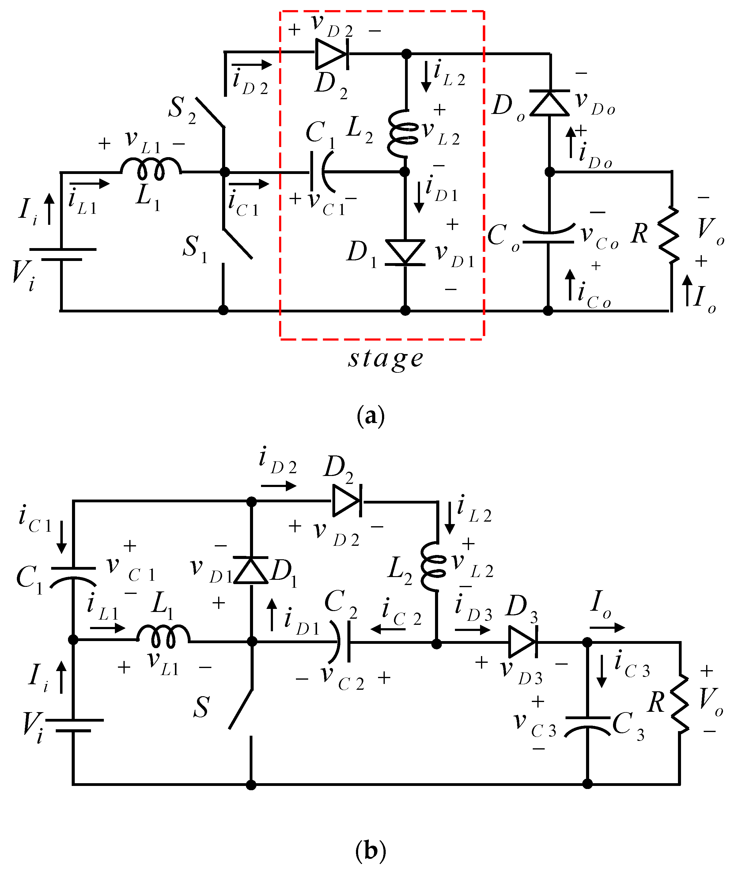
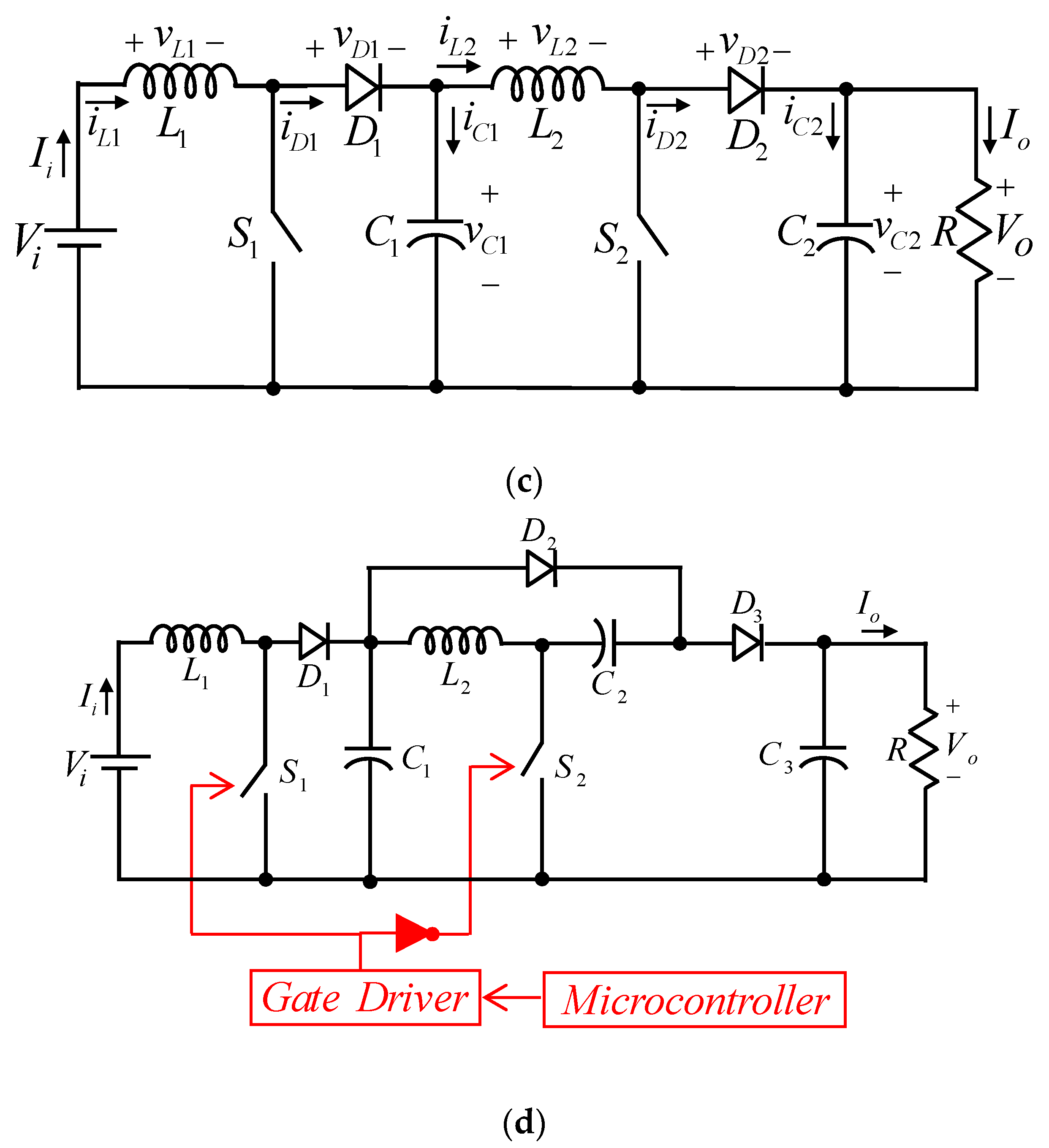
2. The Proposed Converter Structure

Several voltage-lift structures for dc–dc boost converter which have been presented in lecturers are shown in Figure 1a–c [20,21,22]. Additionally, the structure of the proposed converter and its drive circuit are shown in Figure 1d. As shown in Figure 1, the proposed converter has two power electronic switches (such as in [20,22]), two inductors (such as in [20,21,22]), three capacitors and three diodes (such as in [20,21]) and the proposed converter’s driving circuits consist of a microcontroller to providing PWM and a gate driver such as TLP250, a logical IC to generate the opposite PWM wave because the two switches of the proposed converter acts as mutually opposed at a period. The transformer-less and simple structure, direct connection of inductor to the input with lower input current ripple (as filter), lower output capacitance, suitable voltage stress on semiconductors and increasing step-to-step voltage to output are the features of the proposed converter while its drawback is the use of two switches that are switched mutually opposed at a period. For the convenience of analysis, it is intended that:
(a)
The proposed converter is in steady state, and then the output voltage is assumed to be constant;
(b)
The capacitors are large enough and as a result the capacitors voltage can be assumed to be constant in each switching cycle;
(c)
The switches and diodes are ideal.

2.1. Operating Principle
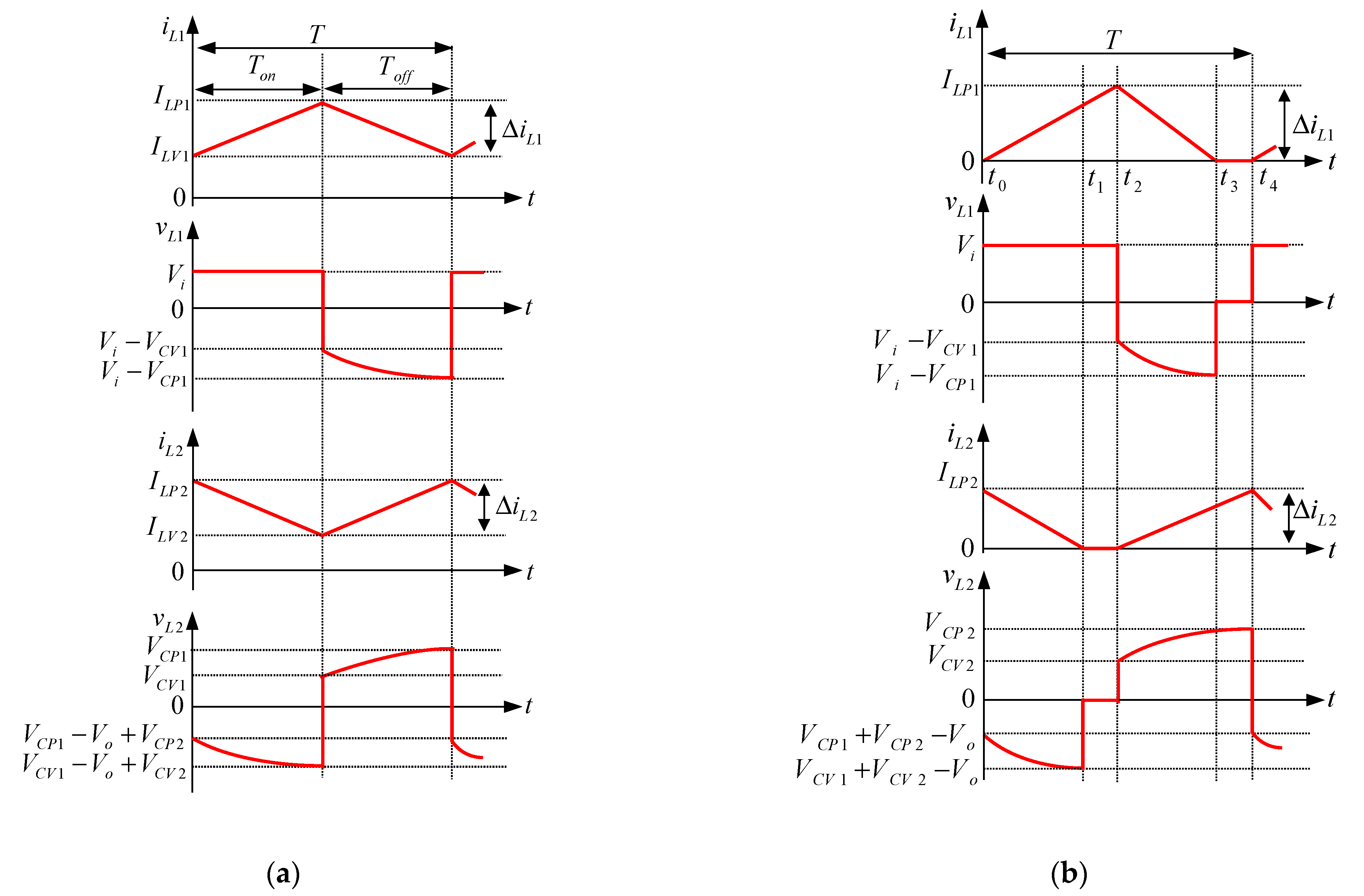
Here, the operating principle of the proposed converter is described with details in CCM and DCM as follows:

2.1.1. The Time Intervals of T o n in CCM and ( t 0 , t 1 ) in DCM:

In this time interval that the switch S 1 is turned on, the switch S 2 is turned off, the diodes of D 1 and D 2 are reversely biased and the D 3 diode is directly biased, the inductor L 1 is directly connected to the input voltage source ( V i ) , as a result, its current is linearly increased from its minimum value ( I L V 1 ) to its maximum value ( I L P 1 ) . During this time interval, the inductor L 2 and the capacitors C 1 and C 2 are connected in series and provided the load current and the capacitor C 3 charge current. In this case, the inductor L 2 current is gradually decreased from its maximum value ( I L P 2 ) to its minimum value ( I L V 2 ) . Additionally, the voltage of the capacitors C 1 and C 2 are decreased from their maximum values ( V C P 1 )   ( V C P 2 ) to their minimum values ( V C V 1 )   ( V C V 2 ) . During this time interval, the capacitor C 3 voltage and its stored energy are increased from its minimum value ( V C V 3 ) to its maximum value ( V C P 3 ) . In DCM, this time interval continues until the current of the inductor L 2 goes to zero.

2.1.2. The Time Interval of ( t 1 , t 2 ) in DCM:

In this time interval, the switch S 1 is still turned on, the switch S 2 is turned off, and the diodes of D 1 and D 2 are reversely biased and as the current the inductor L 2 is zero, therefore, the D 3 diode is reversely biased as well. As a result, the inductor L 1 current is increased to I L P 1 . In addition, the voltage of the capacitors C 1 and C 2 , and their stored energy remain unchanged. In this condition, the load current is provided by the capacitor C 3 discharge current, as a result, its voltage is gradually decreased.

2.1.3. The Time Intervals of T o f f in CCM and ( t 2 , t 3 ) in DCM:

This interval begins when the switch S 1 is turned off and the switch S 2 is turned on. In this state, the diodes of D 1 and D 2 are directly biased while the D 3 diode is still reversely biased. Therefore, the inductor L 1 is connected to the inductor L 2 and the capacitors C 1 and C 2 . As a result, the inductor L 1 current is gradually decreased to I L V 1 while the inductor L 2 current and the voltage of the capacitors C 1 and C 2 is increased to their maximum values. As the load current is provided by the capacitor C 3 discharge current, therefore, the capacitor C 3 voltage is decreased to minimum value. In DCM, this time interval continues until the current of L 1 goes to zero.

2.1.4. The Time Interval of ( t 3 , t 4 ) in DCM:

In this time interval, the switch S 1 is still turned off, the switch S 2 is turned on and the D 3 diode is reversely biased. Due to the fact that the inductor L 1 current is equal to zero, the diodes of D 1 and D 2 are reversely biased. Therefore, the stored energy of the inductor L 2 and the capacitors C 1 and C 2 remains unchanged. On the other hand, the capacitor C 3 stored energy is still released to load, so, the capacitor C 3 voltage is gradually decreased.
In the following sections, indices 1 and 2 represent time intervals of T o n and T o f f in CCM, respectively, and indices 1, 2, and 3 indicate time intervals of ( t 0 , t 1 ) , ( t 1 , t 2 ) and ( t 2 , t 3 ) in DCM, respectively. Additionally, v and i show voltage and current, respectively.

2.2. Analysis of Proposed Converter in CCM

By applying kirchhoff’s voltage law (KVL) in Figure 1d, we would have:
v L 1 , 1 = V i = L 1 d i L 1 , 1 d t = L 1 Δ i L 1 T o n
Applying KVL in Figure 1d, the following is obtained:
v L 1 , 2 = V i v C 1 , 2 = L 1 d i L 1 , 2 d t = L 1 Δ i L 1 T o f f
Applying the voltage-second principle for L 1 , defining duty cycle for dc–dc converter as D = T o n / T and assuming sufficiently large capacitance for C 1 , we get:
v C 1 , 2 = 1 1 D V i = v C 1 = v C 1 , 1
By applying KVL in Figure 1d, we get the following equation:
v L 2 , 1 = v C 1 , 1 + v C 2 , 1 V o = L 2 d i L 2 , 1 d t = L 2 Δ i L 2 T o n
By applying KVL in Figure 1d, the below relation is obtained:
v L 2 , 2 = v C 2 , 2 = L 2 d i L 2 , 2 d t = L 2 Δ i L 2 , 2 T o f f
From Figure 1d and considering sufficiently large capacitance for C 2 , the following relation is obtained:
v C 2 = v C 2 , 1 = v C 2 , 2 = v C 1
According to Figure 1d, the following equation is obtained for the average voltage of the capacitor C 3 :
v C 3 = V o
Applying voltage-second principle for L 2 and substituting (4) and (5), the voltage gain of the proposed converter in CCM is extracted as follows:
M = V o V i = 1 + D D ( 1 D )
Other voltage and current relations in CCM are presented in Table 1. Additionally, the voltage and current waveforms of inductors in CCM are shown in Figure 2a.

2.3. Analysis of the Proposed Converter in DCM

By applying KVL in Figure 1d, we get:
v L 1 , 2 = V i = L 1 d i L 1 , 2 d t = L 1 Δ i L 1 Δ t
By applying KVL in Figure 1d, it is resulted that:
v L 1 , 3 = V i v C 1 , 3 = L 1 d i L 1 , 3 d t = L 1 Δ i L 1 Δ t
At ( t 3 , t 4 ) , the inductor L 1 voltage is equal to:
v L 1 , 4 = 0
Applying the voltage-second principle for L 1 , defining different time intervals in DCM as D 1 = ( t 1 t 0 ) / T , D 2 = ( t 2 t 1 ) / T , D 3 = ( t 3 t 2 ) / T and D 4 = ( t 4 t 3 ) / T , and duty cycle in DCM as D = D 1 + D 2 , the following equation is obtained for the capacitor C 1 :
v C 1 , 3 = D 1 + D 2 + D 3 D 3 = v C 1 , 1 = v C 1 , 2 = v C 1 , 4 = v C 1
By applying KVL in Figure 1d, the below relation is resulted:
v L 2 , 1 = v C 1 , 1 + v C 2 , 1 V o = L 2 d i L 2 , 1 d t = L 2 Δ i L 2 Δ t
The following equation is true for the inductor L 2 voltage at ( t 1 , t 2 ) :
v L 2 , 2 = 0
By applying KVL in Figure 1d, we have:
v L 2 , 4 = v C 1 , 4 = L 2 d i L 2 , 4 d t = L 2 Δ i L 2 Δ t
From Figure 1d and assuming large enough capacity for C 1 , the following equation is derived:
v C 1 = v C 2
From Figure 1d, the below relation can be resulted:
v C 3 = V o
Applying the voltage-second principle for L 2 and substituting (13) to (15), the proposed converter voltage gain in DCM is obtained as follows:
M = V o V i = 1 2 [ 1 + D D + ( 1 + D D ) 2 + 4 D 2 K ]
where K = 2 L 1 R T . Other voltage and current relations in DCM are presented in Table 1. Meanwhile, the voltage and current waveforms of inductors in DCM are shown in Figure 2b.

3. Critical Inductance Calculation

The boundary between CCM and DCM in a dc–dc converter can be determined by the critical inductance. In the proposed converter, the performance can be identified by determining the critical inductance L 1 ( L C 1 ) and L 2 ( L C 2 ) . I L V 1 + I L V 2 = 0 is true for the proposed converter in critical mode. Applying the current-second principle for capacitor C 3 in CCM, the following equations can be derived:
I L P 2 = V i 2 L 2 T + I o D
Substituting (19) into (5) and considering I L V 2 = 0 , yields the following equation for L C 2 :
L C 2 = D 2 ( 1 D ) R 2 ( 1 + D ) f
Applying the current-second principle for capacitor C 1 in CCM, the below relation is obtained:
I L P 1 = V i L 1 T + V o V i I o D
The value of L C 1 is obtained using (2) and (21) as follows:
L C 1 = D 3 ( 1 D ) 2 R 2 ( 1 + D ) 2 f
According to (20) and (22), it can be concluded that L C 2 and L C 1 depends on R , f and D .

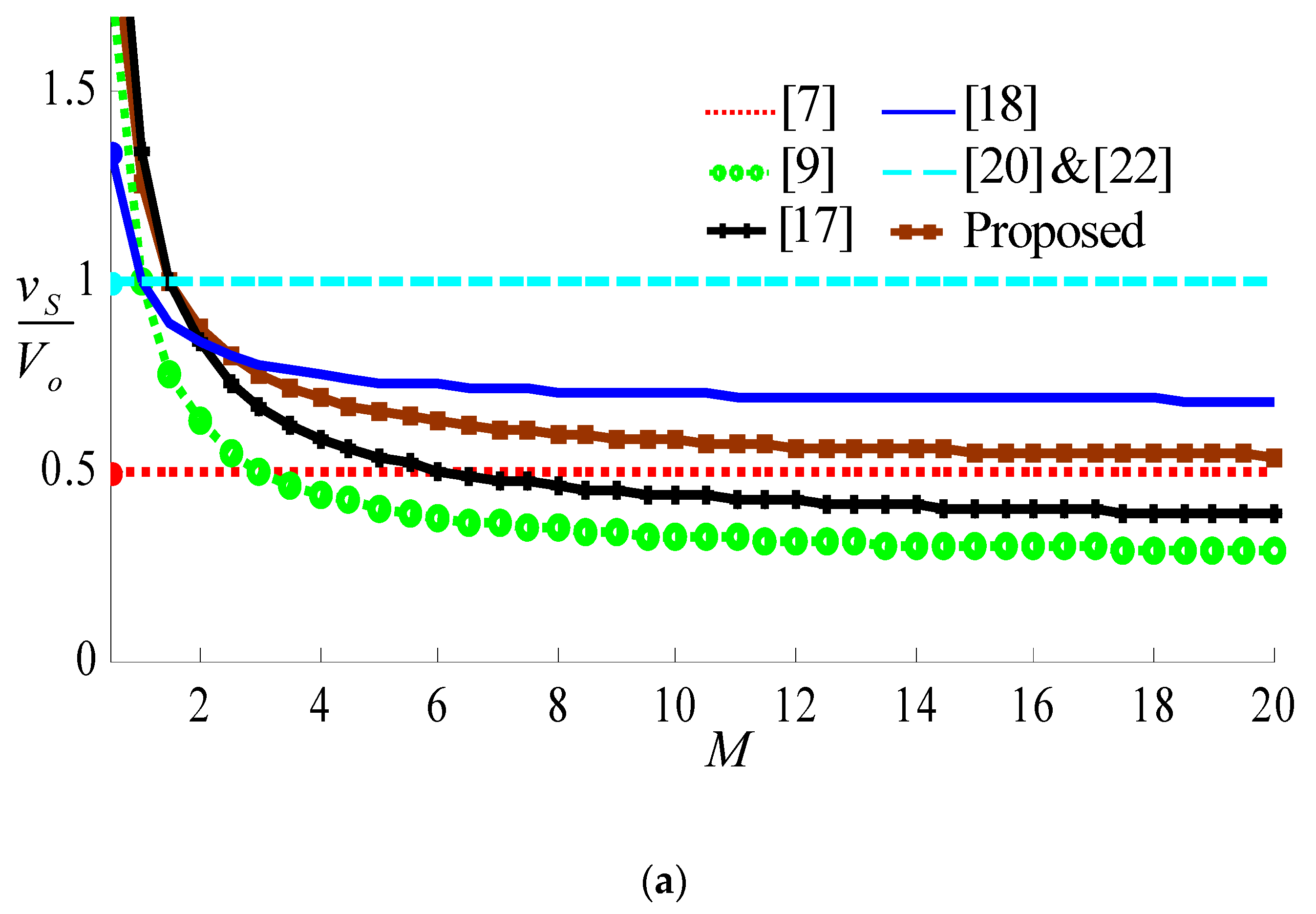
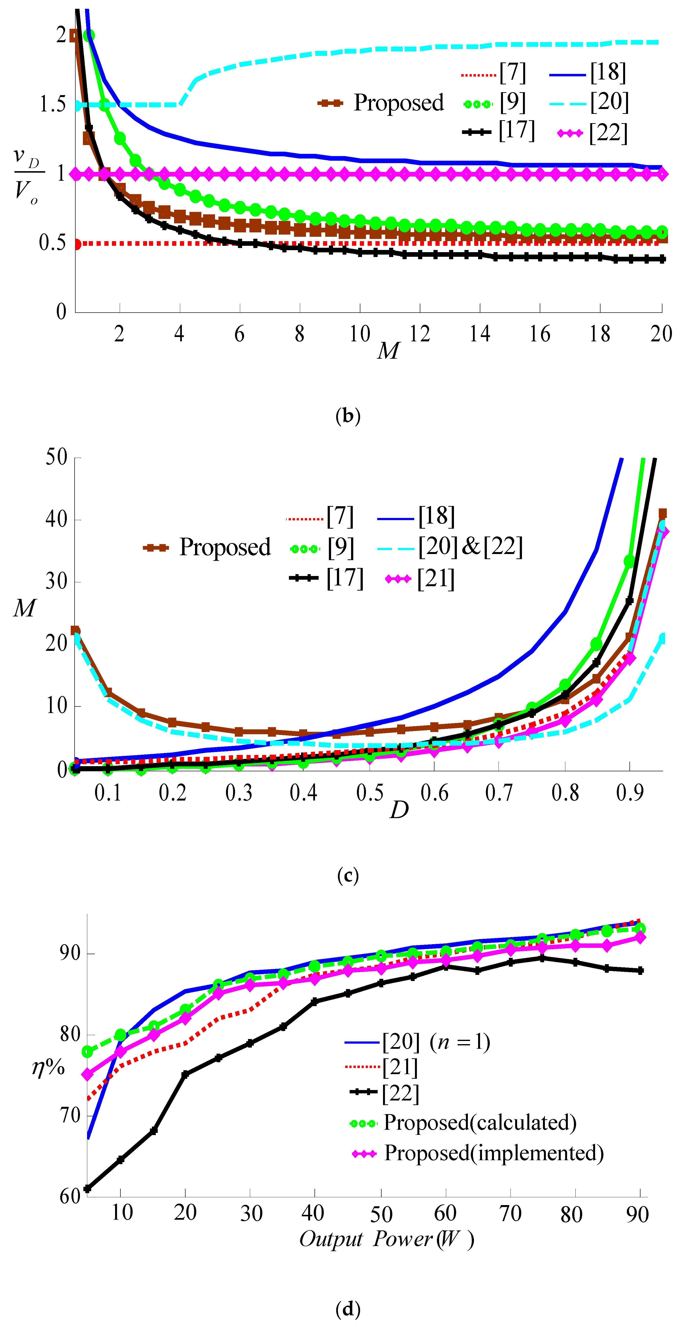
4. Switching Stress Calculation

By appropriate selection of semiconductor elements and switches the cost of a converter can be reduced optimal amount. One of the key devices are power electronics switches and the calculation of peak current flow switch (PCFS) can play an important role in choosing the type of switches. In the following, the PCFS for S 1 and S 2 are discussed.

4.1. Calculation of PCFS in CCM

The current of switch S 1   ( i S 1 ) is increased to its peak value ( i S P 1 C C M ) at t = T o n and is calculated as follows:
i S P 1 C C M = I L P 1
The maximum PCFS of the switch S 1 in CCM ( i S P 1 , max C C M ) is achieved by substituting L 1 = L C 1 as follows:
i S P 1 , max C C M = 2 V o 2 D V i T + V o V i I o D
The PCFS of S 2 in CCM ( i S P 2 C C M ) at t = T o n is as follows:
i S P 2 C C M = I L P 2 + i C 2
Using (19) and considering L 2 = L C 2 , the maximum PCFS of the switch S 1 in CCM ( i S P 2 , max C C M ) is obtained as follows:
i S P 2 , max C C M = V o D T + I o D + i C 2

4.2. Calculation of PCFS in DCM

At t = t 2 , the peak current flow of the switch S 1 in DCM ( i S P 1 D C M ) is equal to:
i S P 1 D C M = I L P 1
At t = t 2 , the peak current flow of the switch S 2 in DCM ( i S P 2 D C M ) is as follows:
i S P 2 D C M = I L P 2 + i C 2

5. Design Consideration

The calculations of the ripples of inductors current and capacitors voltage have a key role in determining the values of the inductors and capacitors, and the values of the inductors and capacitors are determined from these relations. Neglecting inductors current ripple, the root-means-square (rms) of current in CCM, I L 1 and I L 2 , are calculated and shown in Table 2. The allowed range for inductors current ripple, % x L 1 and % x L 2 , are calculated from (1) to (4) and are also shown in Table 2. Considering C 1 = C 2 and | Δ v C 1 | = | Δ v C 2 | , the capacitors voltage ripple in CCM are calculated from (5) and (7).

6. Efficiency Analysis

Neglecting ripples of the inductors current and the capacitors voltage, the root-mean-square (RMS) current relations of inductors and their losses are given as follows:
I L 1 = 1 + D D ( 1 D ) I o
I L 2 = 1 + D 3 D ( 1 D ) I o
P L 1 = r L 1 I L 1 2 + ( K f α B a c β W t f e ) ( 10 3 )
P L 2 = r L 2 I L 2 2 + ( K f α B a c β W t f e ) ( 10 3 )
The diodes RMS current relations are calculated as follows:
I D 1 = 1 + D D 1 1 D I o
I D 2 = 1 + D D 1 ( 1 D ) I o 3
I D 3 = I C 3 + I o = 1 + D 1 D 1 D I o 3
P D 1 = V F 1 I D 1 , a v e + r D 1 I D 1 2 + 0.25 Q r r V D 1 f
P D 2 = V F 2 I D 2 , a v e + r D 2 I D 2 2 + 0.25 Q r r V D 2 f
P D 3 = V F I D 3 , a v e + r D I D 3 2 + 0.25 Q r r V D f
The RMS values of C 1 and C 2 currents are obtained as follows:
I C 1 = I C 2 = I o D + ( 1 + D 3 D ) 2 1 1 D
Considering Q C o + = Q C o , the RMS current of C 3 current is as follows:
I C 3 = I o 1 9 D ( 1 + D 1 D ) 2 + 1 D
The capacitors losses are calculated as follows:
P C n = N = 1 3 r C N I C N 2
The switches RMS current and their losses are equal to:
I S 1 = 1 + D 1 D 1 D I o
I S 2 = 1 + D D 1 1 D 2 I o 3
P S 1 = r D S o n I S 1 2 + 0.5 ( t r + t f ) I S 1 , a v e V S 1 f + 0.5 C O S S V S 1 2 f + 0.25 f Q r r , B D V S 1 + r B D 1 , I B D 1 2 + V B F 1 I B D 1 , a v e
P S 2 = r D S o n I S 2 2 + 0.5 ( t r + t f ) I S 2 , a v e V S 2 f + 0.5 C O S S V S 2 2 f + 0.25 f Q r r , B D V S 2 + r B D 2 , I B D 2 2 + V B F 2 I B D 2 , a v e
Finally, the total loss and efficiency are calculated as follows:
P L o s s = P L 1 + P L 2 + P S 1 + P S 2 + P C n + P D 1 + P D 2 + P D 3
η % = P o u t P o u t + P L o s s × 100

7. Comparison

In this section, the proposed converter is compared with other presented boost dc–dc converters in terms of number of switches, diodes, inductors and capacitors, maximum normalized voltage stresses on switches and diodes, ideal voltage gain, input current ripple and efficiency. The summary of this comparison is shown in Table 3. From the number of active components (switches and diodes), the proposed converter has more active components than [9,17,21,22]. On the other hand, the active components number of the proposed converter is less than [18] and is equal to [7,20]. Of course, the proposed converter has one more switch compared to [17,21]. In terms of passive components (inductors and capacitors), the proposed converter has fewer passive components compared to [9,17,18], and has more compared to [20,22], whereas, the passive components of the proposed converter are equal to [7,21]. Such as in [7,17,20,22], the proposed converter has low input current ripple, while [9,18] has a high current ripple problem. The maximum normalized voltage stresses curve of the switches and diodes are plotted in Figure 3a,b, respectively. As seen in Figure 3a, the maximum normalized voltage stresses of the switches and diodes for the proposed converter are less than [18,20,22], and are higher that [7,17]. Additionally, the maximum normalized voltage stress of the switches for the proposed converter is more than [9] while its maximum normalized voltage stress of the diodes is less than [9]. Comparison of the ideal voltage gain variations with [7,9,17,18,20,21,22] is shown in Figure 3c. As illustrated, the proposed converter provides more ideal voltage gain compared to other for D < 0.5 while the ideal voltage gain of [18] is higher than the proposed converter for 0.5 < D < 0.7 . For D > 0.7 , the proposed converter ideal voltage gain value is more than [7,20,21,22] and is less than [9,17].
The efficiency changes of the proposed converter for different output power are shown in Figure 3d. As shown, the proposed converter has a higher calculated efficiency than [21,22] and its value is less than [20] for lower output power. Increasing output power, the calculated efficiency of the proposed converter reaches to efficiency value in [20,21] while its value gets much better than [22].

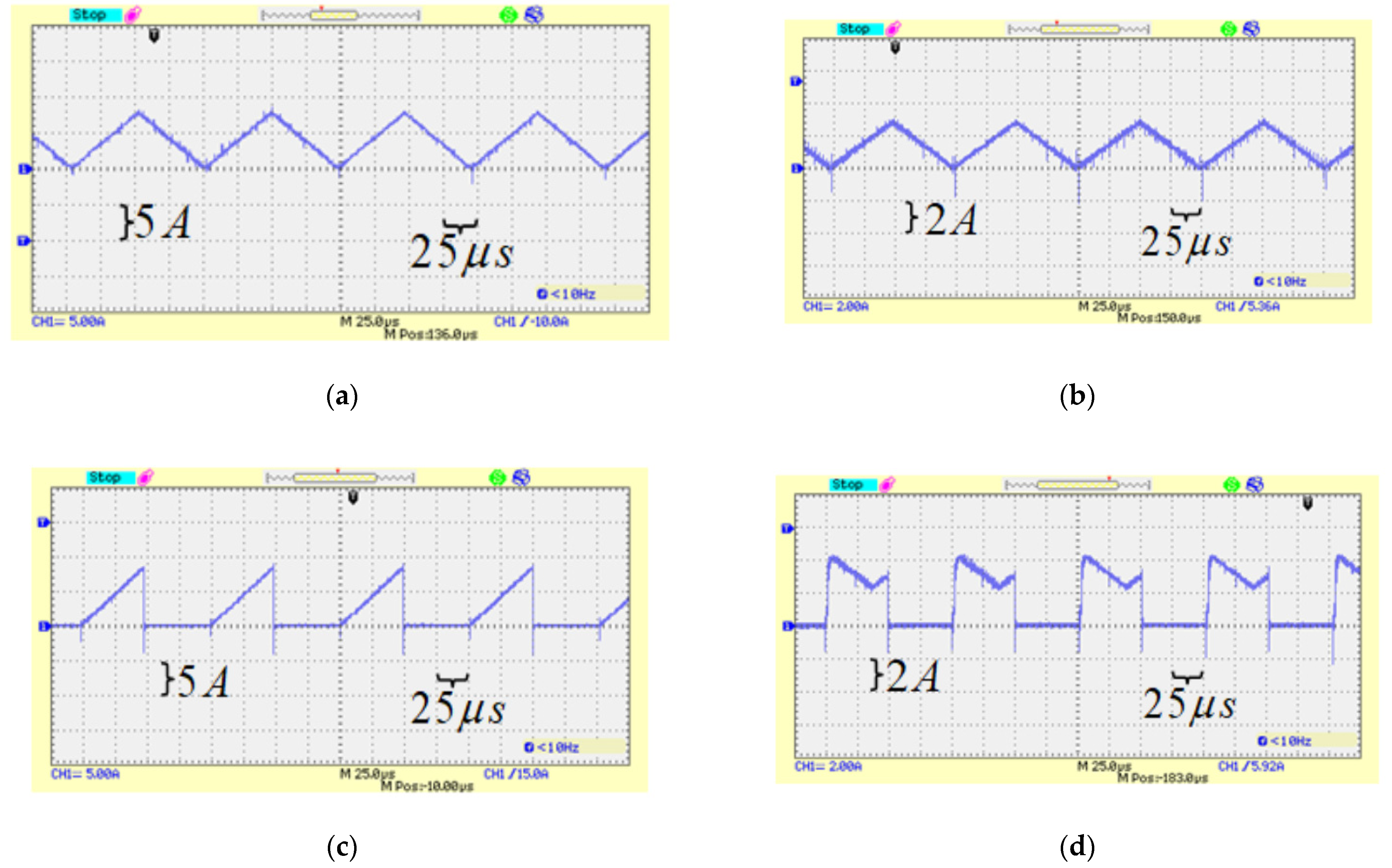
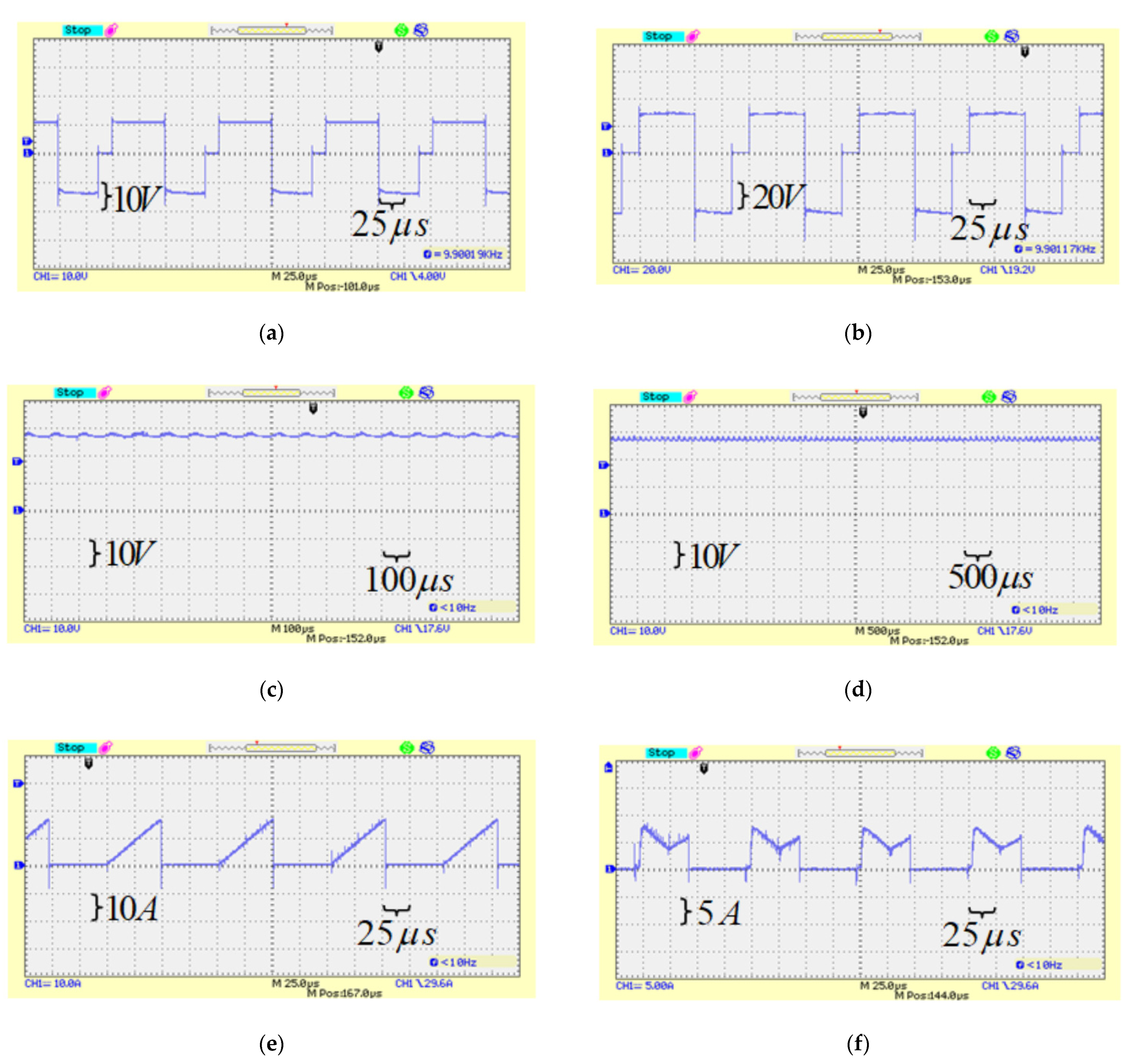
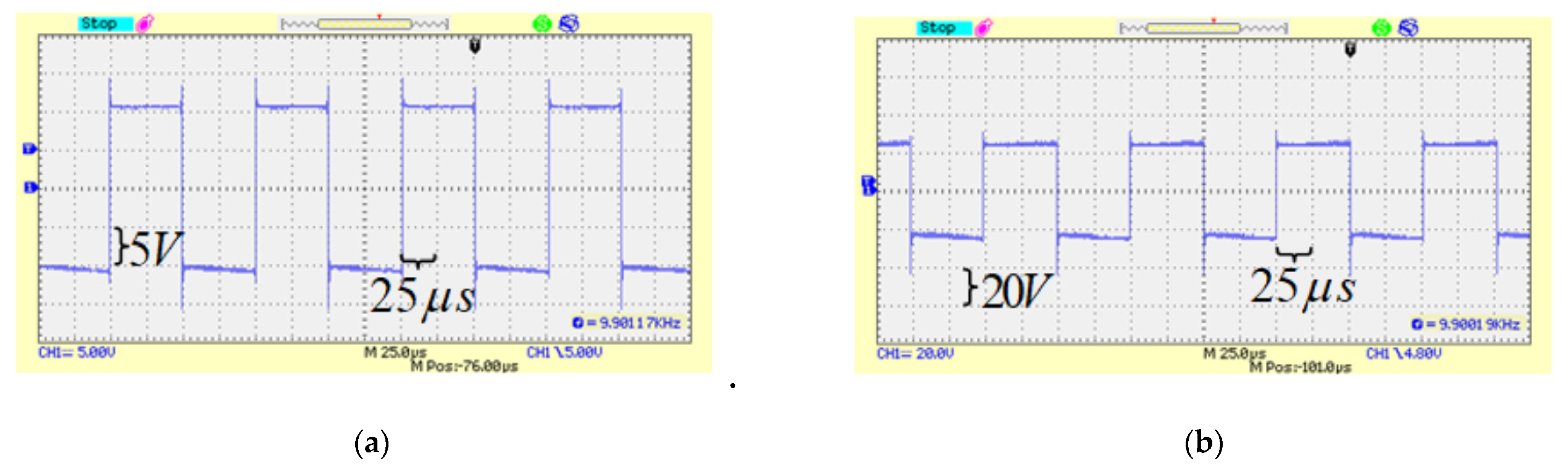
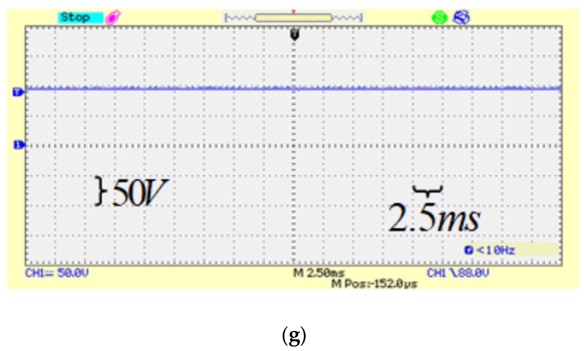
8. Experimental Results

The experimental results by laboratory prototype are used to evaluate the theoretical concepts and relations. The details of experimental laboratory prototype are presented in Table 4. It should be noted that the values of C 1 = C 2 and C 3 are selected from the common values in the market, taking into account Table 2 and % x C 1 = % x C 2 = % 5 and % x C 3 = % 1 . Meanwhile, the core material of the inductors is selected the same in each operating mode. Except for the critical mode and regarding section III, the inductors are designed for free current ripple conditions. In Table 4, K is the eddy current loss coefficient, β a c is the magnetic flux variation, m and n are constant and depend on the core type and W t f e is core weight in grams. Powder core has been selected for all of the inductors. Additionally, r D S o n , t r , t f , t r r , t c , C O S S , Q r r and d i / d t are static drain-source on resistance, rise time, fall time, reverse recovery time, cross-over time, output capacitance, reverse recovery charge and peak diode recovery current slope, respectively.

8.1. Experimental Results for Critical Mode

Considering (20) and (22) and Table 4, the values of L C 1 = 69.4   μ H and L C 2 = 416.6   μ H are obtained. Considering L 1 = L C 1 and L 2 = L C 2 , the proposed converter would be in critical mode. Figure 4a,b show the waveforms of current though the inductors L 1 and L 2 in critical mode, respectively. If L 1 < L C 1 and L 2 < L C 2 then the proposed converter would operates in DCM and the proposed converter operates in CCM for L 1 > L C 1 and L 2 > L C 2 values. Substituting into Table 2 yields i S P 1 , max C C M = 8.15   A and i S P 2 , max C C M = 4   A which the results are verified by Figure 4c,d.

8.2. Experimental Results for CCM

Considering parameters in Table 4, the proposed converter operates in CCM. Some experimental results of the voltage and current of elements are presented in Figure 5. As shown in Figure 5a, the inductor L 1 voltage equals 12   V at T o n (Equation (1)) and it is equal to 14   V at T o f f (Equation (2)). As shown, the voltage of inductor L 2 is equal to 24   V and 24   V at T o n and T o f f , respectively, which confirmed (4) and (5). Substituting the parameters of Table 4 into (3), (6) and (8), yields v C 1 = 24   V , v C 2 = 24   V and v C 3 = 72   V . The calculated values for the capacitors voltage are confirmed by experimental results. As shown in Figure 5e,f, the current variations of the switches S 1 and S 2 are in accordance with Table 2. As illustrated, the PCFS of the switches S 1 and S 2 are equal to i S P 1 C C M = 4.5   A and i S P 2 C C M = 3   A , respectively (Equations (23) and (25)).
Considering the presented parameters in Table 4 into (29) and (47), and from the third term of the diodes losses relations and fifth and sixth terms of switch losses relations yields P L 1 = 2.033   W , P L 2 = 0.4352   W , P C 1 = P C 2 = 0.0512   W , P C 3 = 0.0073   W , P D 1 = 0.1849   W , P D 2 = P D 3 = 0.0256   W , P S 1 = 0.12943   W and P S 2 = 0.7168   W . Thus, the calculated efficiency is 91.4 % , whereas the implemented efficiency is 90.6 % . The calculated and implemented efficiencies for different loads are shown in Figure 3d. As shown, the calculated efficiency of the proposed converter is increased for higher loads and its maximum value are obtained 96.1 % .

8.3. Experimental Results for DCM

Considering presented parameters in Table 4, the proposed converter operates in DCM. Some experimental results in this operating mode are shown in Figure 6. According to Figure 6a, the voltage variations of inductor in one period of time are in accordance with (9), (10) and (11) so that v L 1 , 2 = 12   V , v L 1 , 3 = 16   V and v L 1 , 4 = 0 . Additionally, the relations (13) to (15) are evaluated by experimental results in Figure 6a. As it can be seen, v L 2 , 1 = 42   V , v L 2 , 2 = 0 and v L 2 , 4 = 30   V . In addition, v C 1 = 27   V , v C 2 = 27   V and v C 3 = 94.5   V that verifies (12), (16) and (18), respectively. Furthermore, it is obtained i S P 1 D C M = 18   A and i S P 2 D C M = 7.1   A (see Figure 6e,f) which verifies the accuracy of Table 2. Table 5 shows the summery of experimental results of some parameters under CCM, critical mode and DCM.

9. Conclusions

This paper proposed a new transformer-less structure for a boost dc–dc converter with free and low input current ripple, high voltage gain capability by using an input source, lower output capacitance and suitable voltage stress on semiconductors. This new structure was proposed using the VL technique. For the proposed converter, the voltage and current relations of components were extracted in CCM and DCM in order to design purpose and the output voltage gain was calculated in each operating mode. Additionally, the critical inductance calculations of the proposed converter were presented to operate in critical mode. Moreover, current stress of switches, calculation of passive components values and efficiency are analyzed. Additionally, the proposed converter performance was compared with some other presented converters in terms of the ideal voltage gain in CCM, the number passive and active components, voltage stress on semiconductors, input current conditions and efficiency. As shown, the proposed converter has lower and suitable voltage stress on its semiconductors compared with some presented structures. Additionally, the ideal voltage gain of the proposed converter in CCM was higher than some others in more duty cycles. On the other hand, the proposed converter calculated and implemented maximum efficiencies were increased for higher loads to 96.1 % and 94.8 % , respectively. Of course, a drawback of the proposed converter is the use of two power electronics switches. However, the output voltage gain increased very well. The output voltage for D = D = 50 % , V i = 12   V and f = 10   kHz in CCM and DCM are 72   V and 94.5   V , respectively. The current of switches are obtained as i S P 1 C C M = 4.5   A , i S P 2 C C M = 3   A , i S P 1 , max C C M = 8.15   A , i S P 2 , max C C M = 4   A , i S P 1 D C M = 18   A and i S P 2 D C M = 7.1   A . Finally, the performance of the proposed converter has been reaffirmed with mathematical and experimental results.

Author Contributions

Formal analysis, F.M.S.; Investigation, M.G.; Methodology, M.-H.K. All authors have read and agreed to the published version of the manuscript.

Funding

This research received no external funding.

Institutional Review Board Statement

Not applicable.

Informed Consent Statement

Not applicable.

Conflicts of Interest

The authors declare no conflict of interest.

References

  1. Shahir, F.M.; Babaei, E.; Sabahi, M.; Laali, S. A new dc-dc converter based on voltage lift technique. Int. Trans. Electr. Energy Syst. (ETEP) 2016, 26, 1260–1286. [Google Scholar] [CrossRef]
  2. Farakhor, A.; Abapour, M.; Sabahi, M. Design, analysis, and implementation of a multiport DC–DC converter for renewable energy applications. IET Power Electron. 2019, 12, 465–475. [Google Scholar] [CrossRef]
  3. Shahir, F.M.; Gheisarnejad, M.; Sadabadi, M.S.; Khooban, M.-H. A New Off-board Electrical Vehicle Battery Charger: Topology, Analysis and Design. Design 2021, 30, 7. [Google Scholar]
  4. Saadatizadeh, Z.; Heris, P.C.; Sabahi, M.; Babaei, E. A DC-DC transformerless high voltage gain converter with low voltage stresses on switches and diodes. IEEE Trans. Power Electron. 2019, 34, 10600–10609. [Google Scholar] [CrossRef]
  5. Forouzesh, M.; Siwakoti, Y.P.; Gorji, S.A.; Blaabjerg, F.; Lehman, B. Step-up dc–dc converters: A comprehensive review of voltage-boosting techniques, topologies, and applications. IEEE Trans. Power Electron. 2017, 32, 9143–9178. [Google Scholar] [CrossRef]
  6. Shahir, F.M.; Babaei, E.; Farsadi, M. Analysis and design of voltage-lift technique based non-isolated boost dc-dc converter. IET Power Electron. 2018, 11, 1083–1091. [Google Scholar] [CrossRef]
  7. Wang, P.; Zhou, L.; Zhang, Y.; Li, J.; Sumner, M. Input-parallel output-series dc-dc boost converter with a wide input voltage range, for fuel cell vehicles. IEEE Trans. Veh. Tech. 2016, 62, 7771–7781. [Google Scholar] [CrossRef]
  8. Pajnic, M.; Pejovic, P. Zero-voltage switching control of an interleaved bi-directional buck/boost converter with variable coupled inductor. IEEE Trans. Power Electron. 2019, 34, 9562–9572. [Google Scholar] [CrossRef]
  9. Salvador, M.A.; Lazzarin, T.B.; Coelho, R.F. High step-up dc-dc converter with active switched-inductor and passive switched-capacitor networks. IEEE Trans. Ind. Electron. 2018, 65, 5644–5654. [Google Scholar] [CrossRef]
  10. Taheri, A.; Samsami, H. New topology of a switched-capacitor-based multilevel inverter with a single DC power supply. IET Power Electron. 2019, 12, 1571–1584. [Google Scholar] [CrossRef]
  11. Tseng, K.C.; Lin, J.T.; Huang, C.C. High step-up converter with three-winding coupled inductor for fuel cell energy source applications. IEEE Trans. Power Electron. 2014, 30, 574–581. [Google Scholar] [CrossRef]
  12. Pourjafar, S.; Sedaghati, F.; Shayeghi, H.; Maalandish, M. High step-up DC–DC converter with coupled inductor suitable for renewable applications. IET Power Electron. 2019, 12, 92–101. [Google Scholar] [CrossRef]
  13. Hsieh, Y.P.; Chen, J.F.; Liang, T.J.; Yang, L.S. A novel high step-up DC-DC converter for a microgrid system. IEEE Trans. Power Electron. 2011, 26, 1127–1136. [Google Scholar]
  14. Xian, R.; Liu, X.; Li, F.; Yao, Y.; Geng, N.; Yang, J.; Liu, L.; Sun, Y.; Yue, Z.; Cui, C.; et al. High step-up DC–DC converter with three-winding-coupled-inductor and output capacitor in series for clean energy. IET Power Electron. 2019, 12, 1087–1093. [Google Scholar] [CrossRef]
  15. Zhao, Y.; Li, W.; He, X. Single-phase improved active clamp coupled-inductor-based converter with extended voltage doubler cell. IEEE Trans. Power Electron. 2012, 27, 2869–2878. [Google Scholar] [CrossRef]
  16. Seong, H.W.; Kim, H.S.; Park, K.B.; Moon, G.W.; Youn, M.J. High step-up dc-dc converters using zero-voltage switching boost integration technique and light-load frequency modulation control. IEEE Trans. Power Electron. 2012, 27, 1383–1400. [Google Scholar] [CrossRef]
  17. Banaei, M.R.; Sani, S.G. Analysis and implementation of a new sepic-based single-switch buck-boost dc-dc converter with continuous input current. IEEE Trans. Power Electron. 2018, 33, 10317–10325. [Google Scholar] [CrossRef]
  18. Babaei, E.; Maheri, H.M.; Sabahi, M.; Hosseini, S.H. Extendable nonisolated high gain dc-dc converter based on active-passive inductor cells. IEEE Trans. Ind. Electron. 2018, 65, 9478–9487. [Google Scholar] [CrossRef]
  19. Luo, F.L. Luo-converters, a series of new dc-dc step-up (boost) conversion circuits. Proc. Power Electron. Drive Syst. 1997, 2, 882–888. [Google Scholar] [CrossRef]
  20. Shahir, F.M.; Babaei, E.; Farsadi, M. Extended topology for boost dc-dc converter. IEEE Trans. Power Electron. 2019, 34, 2375–2384. [Google Scholar] [CrossRef]
  21. Shahir, F.M.; Babaei, E.; Farsadi, M. Voltage-lift technique based non-isolated boost dc-dc converter: Analysis and design. IEEE Trans. Power Electron. 2018, 33, 5917–5926. [Google Scholar] [CrossRef]
  22. Shahir, F.M.; Babaei, E.; Farsadi, M. A new structure for nonisolated boost dc-dc converter. J. Circuits Syst. Comput. 2016, 26, 1750012. [Google Scholar] [CrossRef]
  23. Jalilzadeh, T.; Rostami, N.; Babaei, E.; Maalandish, M. Ultra-step-up dc–dc converter with low-voltage stress on devices. IET Power Electron. 2019, 12, 245–257. [Google Scholar] [CrossRef]
Figure 1. (a) The presented converter in [20], (b) the presented converter in [21], (c) the presented converter in [22], (d) the proposed converter.
Automation 02 00014 g001aAutomation 02 00014 g001b
Figure 2. The voltage and current waveforms for inductors: (a) in CCM; (b) in DCM.
Automation 02 00014 g002
Figure 3. Compression between different converters: (a) maximum normalized voltage stress on switches, (b) maximum normalized voltage stress on diodes, (c) ideal voltage gain variation in versus duty ratios, (d) efficiency variations.
Automation 02 00014 g003aAutomation 02 00014 g003b
Figure 4. The current waveforms in a critical mode for; (a) L 1 current, (b) L 2 current; (c) S 1 current, (d) S 2 current.
Automation 02 00014 g004
Figure 5. Experimental results in CCM: (a) L 1 voltage; (b) L 2 voltage; (c) C 1 voltage; (d) C 2 voltage; (e) S 1 current; (f) S 2 current; (g) C 3 voltage.
Automation 02 00014 g005aAutomation 02 00014 g005b
Figure 6. Experimental results in DCM: (a) L 1 voltage; (b) L 2 voltage; (c) C 1 voltage; (d) C 2 voltage; (e) S 1 current; (f) S 2 current; (g) C 3 voltage.
Automation 02 00014 g006aAutomation 02 00014 g006b
Table 1. The voltage and current equations of elements in CCM and DCM.
Element/Time IntervalCCMDCM
T o n T o f f ( t 0 , t 1 ) ( t 1 , t 2 ) ( t 2 , t 3 ) ( t 3 , t 4 )
C 1 i C 1 , 1 = i C 2 , 1 = i L 2 , 1 i C 1 , 2 = i L 1 , 2 i L 2 , 2 i C 2 , 2 i C 1 , 1 = i C 2 , 1 = i L 2 , 1 0 i C 1 , 3 = i L 1 , 3 i C 2 , 3 i L 2 , 3 0
C 2 i C 1 , 1 = i C 2 , 1 = i L 2 , 1 i C 2 , 2 = i L 1 , 2 i L 2 , 2 i C 1 , 2 i C 1 , 1 = i C 2 , 1 = i L 2 , 1 0 i C 2 , 3 = i L 1 , 3 i L 2 , 3 i C 1 , 3 0
C 3 i C 3 , 1 = i L 2 , 1 I o i C 3 , 2 = I o i C 3 , 1 = i L 2 , 1 I o i C 3 , 4 = I o
D 1 v D 1 , 1 = v C 1 , 1 i D 1 , 2 = i L 2 , 2 + i C 1 , 2 v D 1 , 2 = v C 1 , 2 i D 1 , 3 = i L 1 , 3 i C 2 , 3 v D 1 , 4 = V i v C 1 , 4
D 2 v D 2 , 1 = v C 1 , 1 v C 2 , 1 + v L 2 , 1 i D 2 , 2 = i C 2 , 2 v D 2 , 2 = v C 1 , 2 v C 2 , 2 v L 2 , 2 i D 2 , 3 = i L 1 , 3 i C 1 , 3 i L 2 , 3 v D 2 , 4 = V i v C 2 , 2
D 3 i D 3 , 1 = i L 2 , 1 v D 3 , 2 = v C 2 , 3 V o i D 3 , 1 = i L 2 , 1 v D 3 , 4 = v C 2 , 4 V o
S 1 i S 1 = i L 1 v S 1 = V i v L 1 , 2 i S 1 = i L 1 v S 1 = V i v L 1 , 3 v S 1 = V i
S 2 v S 2 = v C 1 , 1 v L 2 , 1 i S 2 = i L 2 + i C 2 v S 2 = v C 1 , 1 v L 2 , 1 v S 2 = v C 1 , 2 i S 2 = i L 2 + i C 2 v S 2 = v C 1 , 4 v L 2 , 4
Table 2. Ripples calculations for inductors current and capacitors voltage.
ElementRelation
L 1 I L 1 = ( 1 + D ) 2 D 2 ( 1 D ) 2 V i R % x L 1 = Δ i L 1 I L 1 = D 3 ( 1 D ) 2 R L 1 f ( 1 + D ) 2
L 2 I L 2 = D ( 1 + D ) D 2 ( 1 D ) 2 V i R % x L 2 = Δ i L 2 I L 2 = D ( 1 D ) 2 R L 2 f ( 1 + D )
C 1 = C 2 | Δ v C 1 | = | Δ v C 2 | = D 2 C 1 f [ ( 1 + D ) V i D 2 ( 1 D ) 2 R ] % x C 1 = % x C 2 = | Δ v C 1 | v C 1 = D ( 1 + D ) 2 R C 1 f D 2 ( 1 D )
C 3 | Δ v C 3 | = I o ( 1 D ) C 3 f % x C 3 = | Δ v C 3 | v C 3 = 1 D R C 3 f
Table 3. Comparison between different converters.
Element/Ref.[7][9][17][18][20] (n = 1)[21][22]Proposed
Active componentswitch22132122
diode323123323
Passive componentinductor23462222
capacitor33612323
Input ripple currentLowHighLowHighLowLowLowLow
Max. voltage stress of switches 1 2 3 + M 4 M 3 + M 3 M 1 + 2 M 3 M 1 1 + M 2 1 3 + 2 M 4 M
Max. voltage stress of diodes 1 2 3 + M 2 M 3 + M 3 M 1 + M M 3 2 + 1 4 1 M 1 + M 2 1 3 + 2 M 4 M
Voltage gain in CCM ( M ) 2 1 D 1 + 3 D 1 D 3 D 1 D 1 + 5 D 1 D 1 D ( 1 D ) 1 + D 1 D 1 D ( 1 D ) 1 + D D ( 1 D )
Voltage gain variation ( D : 0 0.9 ) 2 20 1 37 0 27 1 55 11 19 11 21
Table 4. Experimental parameters.
ParametersCCMDCM
L 1
(Powder core)
L 1 = 3   mH ; r L 1 = 0.17   Ω L 1 = 35   μ H ; r L 1 = 0.002   Ω
K = 0.00551 ; α = 1.23 ; β = 2.12 ; W t f e = 44.6 ; B a c = 0.0527 K = 0.00551 ; α = 1.23 ; β = 2.12 ; W t f e = 44.6 ; B a c = 0.0527
L 2
(Powder core)
L 2 = 1.5   mH ; r L 2 = 0.11   Ω L 2 = 250   μ H ; r L 2 = 0.004   Ω
K = 0.00551 ; α = 1.23 ; β = 2.12 ; W t f e = 39.1 ; B a c = 0.0545 K = 0.00551 ; α = 1.23 ; β = 2.12 ; W t f e = 39.1 ; B a c = 0.0545
C 1 = C 2 & C 3 110   μ F ; r C 1 = 0.02   Ω & 63   μ F ; r C 3 = 0.015   Ω
Diodes Type :   MUR 1560 ; V F , D = 0.8   V ; r D = 0.01   Ω
N-channel MOSFET Type :   STW 45 NM 50 F ; r D S o n = 0.07   Ω ; t r = 11   nS ; t f = 25   nS t r r = 245   nS ; t c = 44   nS ; C O S S = 1260   pF ; Q r r = 1600   nC ; d i / d t = 100   A / μ S
V i , f , D , D , R 12   V , 10   kHz , 50 % , 50 % , 100   Ω
Output Power 51.8   W 89.3   W
Table 5. Summary of experimental results for different operating modes.
ParametersCCMCritical ModeDCM
i S P 1 , max 4.5 A8.15 A18 A
i S P 2 , max 3 A4 A7.1 A
i L 1 , max -8 A-
i L 2 , max -3 A-
v C 1 24-27
v C 2 24-27
v C 3 72-94
Publisher’s Note: MDPI stays neutral with regard to jurisdictional claims in published maps and institutional affiliations.

