Article

An Efficient Electrostatic Discharge Analytical Model for a Local Bottom-Gate Carbon Nanotube Field-Effect Transistor

1
School of Opto-Electronic and Communication Engineering, Xiamen University of Technology, Xiamen 361024, China
2
School of Electronics, Peking University, Beijing 100049, China
3
Jade Bird Fire Co., Ltd., Beijing 100871, China
*
Author to whom correspondence should be addressed.
Electron. Mater. 2025, 6(4), 17; https://doi.org/10.3390/electronicmat6040017
Submission received: 9 September 2025 / Revised: 14 October 2025 / Accepted: 21 October 2025 / Published: 23 October 2025
(This article belongs to the Special Issue Feature Papers of Electronic Materials—Third Edition)

Abstract

In the post-Moore era, carbon nanotube field-effect transistors (CNTFETs) are a promising alternative to complementary metal-oxide-semiconductor (CMOS) technology at and below the 5 nm node. Compact models bridge circuit design and device physics, yet the electrostatic discharge (ESD) behavior of CNTFETs remains insufficiently captured. Focusing on the local bottom-gate (LBG) CNTFET structure, which offers enhanced gate control due to its bottom-gate configuration, this paper investigates three dominant ESD-triggering mechanisms—thermionic current, tunneling leakage current, and thermal failure breakdown. Then, a hybrid compact–behavioral ESD model for CNTFETs is established. After theoretical derivation and comparison with test results, the model parameters are optimized through fitting. The simulation results exhibit excellent agreement with CNTFET measurements, particularly capturing the Human Body Model (HBM) pre-charge threshold phenomenon at 72 V and accurately predicting the subsequent voltage collapse behavior. This validates the accuracy and effectiveness of the model, laying a theoretical and experimental foundation for further construction of carbon-based standard-cell and I/O libraries.

1. Introduction

As integrated circuit process continues to evolve towards 5 nm and even more advanced technology nodes, traditional silicon-based metal-oxide-semiconductor field-effect transistors (MOSFETs) are facing multiple physical bottlenecks caused by short channel effects, quantum tunneling effects, and weakened gate to channel electrostatic control capabilities [1]. Even with the introduction of three-dimensional transistor structures such as FinFET, the performance improvement space in subthreshold swing, turn-on current, and scaling of gate length has approached the theoretical limit [2].
In this context, carbon nanotube field-effect transistors (CNTFETs) offer a promising alternative to current silicon-based processes, particularly as technology moves beyond the 5 nm node. CNTFETs feature significantly higher carrier mobility (>1000 cm2/Vs), compared to silicon’s typical mobility of 400 cm2/Vs, enabling faster switching speeds and better energy efficiency. Their unique material properties, including outstanding electronic transport mechanisms and a current density up to 10 times higher than that of silicon, allow CNTFETs to achieve superior performance in high-speed and low-power applications [3]. To exemplify device-level feasibility under aggressive scaling, Franklin et al. demonstrated sub-10 nm CNTFETs with a local bottom-gate stack (W gate/3 nm HfO2, Pd S/D), showing competitive low-voltage performance versus contemporary silicon transistors [4].
In recent years, significant progress has been made in the development of CNTFET technology. Research has shown that at the 32 nm process node, the driving current of CNTFET can be increased by about 100% compared to the same generation silicon-based devices [5]. In high-speed digital circuit applications, the CNTFET exhibits significant energy efficiency advantages [6]. In addition, in the field of biomedical sensing, CNTFET gene sensors have achieved extremely high detection sensitivity at the femtomolar (fM) level, providing a new technological path for instant medical diagnosis [7]. In the field of three-dimensional integration and heterogeneous packaging, the unique structure of the CNTFET shows great potential and is expected to break through the density limitations of traditional planar integrated circuits [8]. More importantly, at the level of commercial manufacturing, researchers have successfully achieved large-scale preparation of CNTFETs in existing silicon manufacturing facilities, laying a solid foundation for the industrial application of CNTFETs [9]. These research advances clearly indicate that the CNTFET is gradually moving from the laboratory exploration stage to practical applications, and its inherent advantages in device performance, power consumption, and integration density are being increasingly widely verified through experiments. However, in order to achieve mature applications of the CNTFET in very large-scale integrated circuits (VLSI), the reliability of the devices is a core challenge that urgently needs to be addressed [10]. Especially in the trend of continuous scaling and high-density integration of devices, electrostatic discharge (ESD) protection has become one of the important technical bottlenecks that restrict the practical application of CNTFETs.
Yao et al. investigated the intrinsic transport properties of single-wall carbon nanotubes (SWCNTs) in high electric field environments [11]. In 2013, Shrivastava et al. conducted the first systematic study on the ESD characteristics of multi-walled carbon nanotubes (MWCNTs) and discovered their unique subsequent shell burning mechanism [12]. However, due to the significant electrical performance differences between SWCNTs and MWCNTs, the results of this study did not directly reveal the ESD behavior of CNTFETs. Until 2025, Duan et al. studied the ESD characteristics of SWCNTs with transmission line pulse (TLP) testing equipment to conduct an HBM test. By 2025, Duan et al. completed a comprehensive study on the ESD characteristics of SWCNTs and, for the first time, discovered and confirmed the three-stage ESD failure process of CNTFETs [13]. Although these studies have laid the foundation for the ESD theory of the CNTFET, there is still insufficient research on ESD devices and circuit design in carbon-based integrated circuits.
The ESD design of traditional silicon-based integrated circuits mainly relies on the experience accumulation of designers and repeated chip verification. This method is not only time-consuming and costly, but also difficult to adapt to the increasingly complex protection requirements of modern integrated circuits [14,15]. In order to improve this problem, researchers have developed a modeling method for the high-voltage transient characteristics of silicon-based devices and have used the established model in circuit-level simulations to pre-validate the effectiveness of ESD schemes. It significantly improves design efficiency and reduces trial-and-error costs [16,17,18]. However, the CNTFET uses quasi one-dimensional carbon nanotubes as the conductive channel, and its carriers exhibit quasi-ballistic transport characteristics, which are fundamentally different from the transport mechanism in traditional MOSFETs [19]. This fundamental difference prevents ESD structures such as gate-grounded NMOS (GGNMOS), which are widely used in silicon-based processes, from being directly transplanted into carbon-based processes.
Meanwhile, the experience accumulated by designers in the field of silicon-based ESD is also difficult to directly apply to the design of carbon-based ESD circuits. More importantly, current research on compact models of CNTFETs mainly focuses on the characteristics of its normal operating voltage range, while there is a clear gap in the description of the device’s behavior under high-voltage, high-current transient shocks such as ESD [20,21,22,23,24]. Therefore, establishing an accurate model specifically for the high-voltage transient characteristics of CNTFET has crucial theoretical and practical significance. This model can not only assist designers in pre-evaluating the effectiveness of carbon-based ESD schemes but also provide a solid theoretical basis for the systematic and automated design of future carbon-based ESD circuits.
Based on the current research status and challenges in the field of carbon-based electronics, this study establishes an ESD model for the CNTFET, targeting three main triggering mechanisms: thermionic current, tunneling leakage current, and thermal failure breakdown. At the same time, the model is simulated. By comparing the test results with the CNTFET, the accuracy and effectiveness of the model are verified, which lays a theoretical and experimental foundation for further construction of carbon-based standard cell and IO libraries.

2. ESD Modeling of CNTFET

A typical CNTFET structure is mainly composed of carbon nanotubes as conductive channels, a gate, a source, and a drain. The electric field applied through the gate can effectively regulate the transport of charge carriers in the CNT channel. According to the geometric layout of the gate relative to the CNT channel, CNTFET devices can be mainly divided into three mainstream structures: bottom-gate (BG), top-gate (TG), and gate-all-around (GAA). The gate of the BG-CNTFET is located on the substrate below the CNT channel and isolated from the channel by a dielectric layer. The manufacturing process of such devices is relatively simple. However, due to the typically thick gate dielectric layer, the electrostatic control ability of the gate over the channel is relatively limited, making it more commonly used in low-frequency analog circuits [25]. The TG-CNTFET directly deposits a high-k gate dielectric above the CNT channel, which can significantly enhance gate control capability and increase driving current. Therefore, it is widely used in the design of high-performance logic circuits and carbon–silicon-heterojunction-integrated static random access memory (SRAM) cells [26]. The GAA-CNTFET has the best electrostatic control capability and excellent suppression performance for short-channel effects. However, its manufacturing process is extremely complex and requires precise alignment technology at the nanoscale. Currently, it is mainly aimed at cutting-edge applications such as ultra-low power nanoelectronic devices and emerging quantum computing units [27].
The selection of device structure is crucial when conducting ESD characteristic research and modeling. TG- and GAA-CNTFETs typically use ultra-thin high-k gate dielectrics to achieve strong gate control capabilities. However, such ultra-thin dielectrics are more prone to charge trap accumulation and soft breakdown within the gate oxide layer when subjected to high-voltage transient impacts caused by ESD, which may lead to premature device failure. In contrast, local-bottom-gate (LBG)-CNTFETs typically use relatively thick oxides as the back gate dielectric, which gives them higher gate voltage tolerance and is more advantageous for ESD protection. In addition, considering the high requirements of ESD modeling and experimental testing for inter-batch parameter uniformity and process stability, this study selected an LBG-CNTFET with a relatively mature process as the research object. The schematic cross-section of the device is shown in Figure 1.
Pd is used as the source/drain contact metal, and the gate electrode consists of Ti/Au. Above the local bottom gate, a dielectric stack of Y2O3/HfO2 is deposited, followed by placement of the carbon nanotube channel and subsequent deposition of source/drain metals. In certain regions, the source/drain metal partially overlaps with the gate metal. The channel length is 4 µm, and the channel width is 30 µm. Following device fabrication, a surface electrical modification layer is deposited to electrostatically dope the transistor into n-type. Then, wet etching is applied to remove this modification layer in regions intended to retain p-type contact. Finally, an electron-beam resist passivation layer is deposited over the device.
CNTFET exhibits significant quantum confinement effects due to its unique one-dimensional electronic structure. Compared with traditional silicon-based transistors with three-dimensional or two-dimensional channels, the phonon scattering inside CNTs is relatively weak and usually has a lower defect density. These characteristics enable the mean free path (MFP) of charge carriers in CNT channels to reach hundreds of nanometers or even micrometers. When the effective channel length of CNTFET (i.e., the effective carrier transport distance between source and drain) is less than or close to this MFP, the scattering events experienced by carriers during transport are minimal, and their behavior will exhibit typical quasi-one-dimensional ballistic transport or near ballistic transport characteristics. In theory, this transport process can be accurately described by the Landauer–Büttiker formula [28,29].
I D = 4 q h ν T ( E ) [ f ( E E f , s ) f ( E E f , d ) ] d E
Among them, q is the unit charge, and h is Planck’s constant. Constant term 4 comes from the two conduction bands and spin degeneracy of CNT, and v represents the number of effective sub-bands involved in conduction. T(E) represents the quantum transmission probability at energy E, and Ef,s and Ef,d are the Fermi energy of the source and drain, respectively. f ( E E f , s ) and f ( E E f , d ) are the Fermi–Dirac distribution functions at the source and drain, respectively. Based on this, the equivalent circuit model of CNTFET can be represented as shown in Figure 1.
Directly solving Equation (1), which involves complex transmission probability calculations and high-dimensional energy integration, poses significant challenges in terms of computational efficiency and convergence for mainstream SPICE simulators. Especially when the circuit scale and the number of devices increase, direct calculation will lead to an exponential increase in simulation time, which cannot meet the actual needs of integrated circuit design. Therefore, in order to efficiently and accurately describe the electrical characteristics of the CNTFET in circuit-level simulation, especially its behavior under extreme conditions such as ESD, it is crucial to develop accurate and efficient Compact Models.

2.1. Thermionic Current Modeling

In typical CNTFETs, when the gate voltage is higher than the threshold voltage, its drain current is mainly contributed by the thermionic emission carriers injected from the source and crossing the top of the channel barrier. Based on the widely used Virtual Source (VS) model theoretical framework [21], the drain current can be expressed as the product of the moving charge density at the virtual source location (i.e., the top of the potential barrier) and the effective injection velocity of charge carriers at that location.
I D = q n v s v v s
n v s is the effective surface density or line density of moving electrons (or holes) at the virtual source, and v v s is the average effective velocity of the corresponding charge carriers at the virtual source. The gate voltage controls n v s by adjusting the height of the channel potential barrier. n v s depends on the series voltage divider effect of the gate oxide capacitor C o x and the CNT’s own quantum capacitance C q . Due to the quasi-one-dimensional band structure of carbon nanotubes, their density of states (DOS) is relatively low, resulting in a quantum capacitance C q of the same magnitude as Cox, which cannot be ignored. Therefore, under strong inversion conditions, the equivalent gate capacitance C i n v of the channel cannot be simply approximated as Cox and needs to be calculated through a series model.
C i n v = C o x C q , e f f C o x + C q , e f f
C q , e f f is the equivalent quantum capacitance used to approximate the one-dimensional quantum capacitance effect under strong gate bias conditions. In compact models, C q , e f f is often expressed using empirical or semi-empirical formulas:
C q , e f f = A q c E g / ( k B T ) + B q c
Among them, E g is the bandgap of carbon nanotubes, k B   is the Boltzmann constant, T is the absolute temperature, and parameters A q c and B q c are empirical fitting parameters. Their values need to be calibrated with experimental data to ensure the accuracy of the model under different diameters, temperatures, and bias conditions. A q c mainly reflects the maximum quantum capacitance of one-dimensional channels limited by the low density of states, while B q c can characterize a residual constant term or a non-ideal effect of quantum capacitance under high electric fields. Through C i n v , we can approximately assume that under strong inversion conditions, the channel charge density q n v s generated by the virtual source satisfies
q n v s C i n v ( V g s V t Δ ϕ )
Δ ϕ = δ V d s
V g s is the gate source voltage, and V t is the threshold voltage. Δ ϕ is an effective barrier modulation term, which is mainly used to describe the Drain-Induced Barrier Lowering (DIBL) effect caused by the drain source voltage V d s . When V d s increases, the barrier of the drain decreases, manifested as a decrease in the effective threshold voltage with the increase of V d s . In (6), we describe this effect using the DIBL coefficient δ . It reflects the electrostatic shielding and the gate’s ability to control the channel. It is usually extracted from the rate of change in the threshold voltage with V d s in the device’s output characteristic.
The above charge model, based on a linear capacitor (Equation (5)), is mainly effective in a strong inversion region. In the subthreshold region, the carrier concentration varies exponentially with gate voltage, and the thermionic current also follows an exponential law. In order to uniformly describe the process from subthreshold to strong inversion, a smoothing function is introduced to continuously describe the electron density at the virtual source, as well as the thermoelectric coefficient ϕ T = k B T / q and subthreshold slope factor n s s , so that the electron density model at the virtual source can be represented as
n v s = C i n v q n s s ϕ T ln [ 1 + exp ( V g s V t δ V d s n s s ϕ T ) ]
When V g s V t δ V d s is much greater than 0, the device is a strong inversion region; when n v s C i n v q ( V g s V t δ V d s ) , the device recovers to a linear capacitor model; when V g s V t δ V d s is less than 0, then
n v s C i n v q n s s ϕ T exp ( ( V g s V t δ V d s ) / ( n s s ϕ T ) )
Equation (8) clearly presents the characteristic of subthreshold current increasing exponentially with gate voltage. By calibrating the subthreshold factor n s s , Equation (7) can accurately fit the I-V characteristics obtained from experimental data, achieving a smooth and continuous transition between weak and strong inversion regions.
In a short-channel CNTFET, due to significant suppression of carrier scattering, the injected carriers from the source can be largely regarded as quasi-ballistic transport. v v s is the initial effective velocity at which these charge carriers are injected into the channel. According to the widely used virtual source model, v v s is influenced by both the intrinsic ballistic limit velocity of carbon nanotubes and the scattering events within the channel (characterized by the equivalent mean free path λ v ). By approximating through empirical formulas, we can obtain
v v s = λ v λ v + 2 L g v B
L g is gate length, λ v is equivalent mean free path, and v B is defined as the theoretical upper carrier velocity in CNTs under a fully ballistic transport ceiling ( v B = 8.0 × 1 0 5 m / s ).
To describe the smooth transition of the drain current I d from the linear to the saturation region, it is necessary to introduce a dependence on V d s . Combining Equations (2), (7), and (9), and considering the current saturation effect, a complete expression for the drain current is constructed as shown in Equation (10). In the unsaturated region, the current increases with the increase of V d s ; when V d s is large enough, the electric field distribution near the virtual source tends to saturate, and the current also saturates accordingly. Finally, by introducing the low field effective mobility μ and empirical smoothing parameter β to regulate the steepness of the transition from linear to saturation region, the following form of current equation can be obtained:
I d = q n v s μ V d s L g 1 + μ V d s L g v v s β 1 / β
We modeled and simulated the current characteristics dominated by the ballistic transport of the CNTFET within the normal operating voltage range, and the simulation results are shown in Figure 2. The main parameter settings used in the model are listed in Table 1. This model, through reasonable physical approximation and parameter extraction, can effectively describe the DC characteristics of the CNTFET under normal operating voltage (0 V~2 V) while ensuring computational efficiency.

2.2. Tunneling Current Modeling

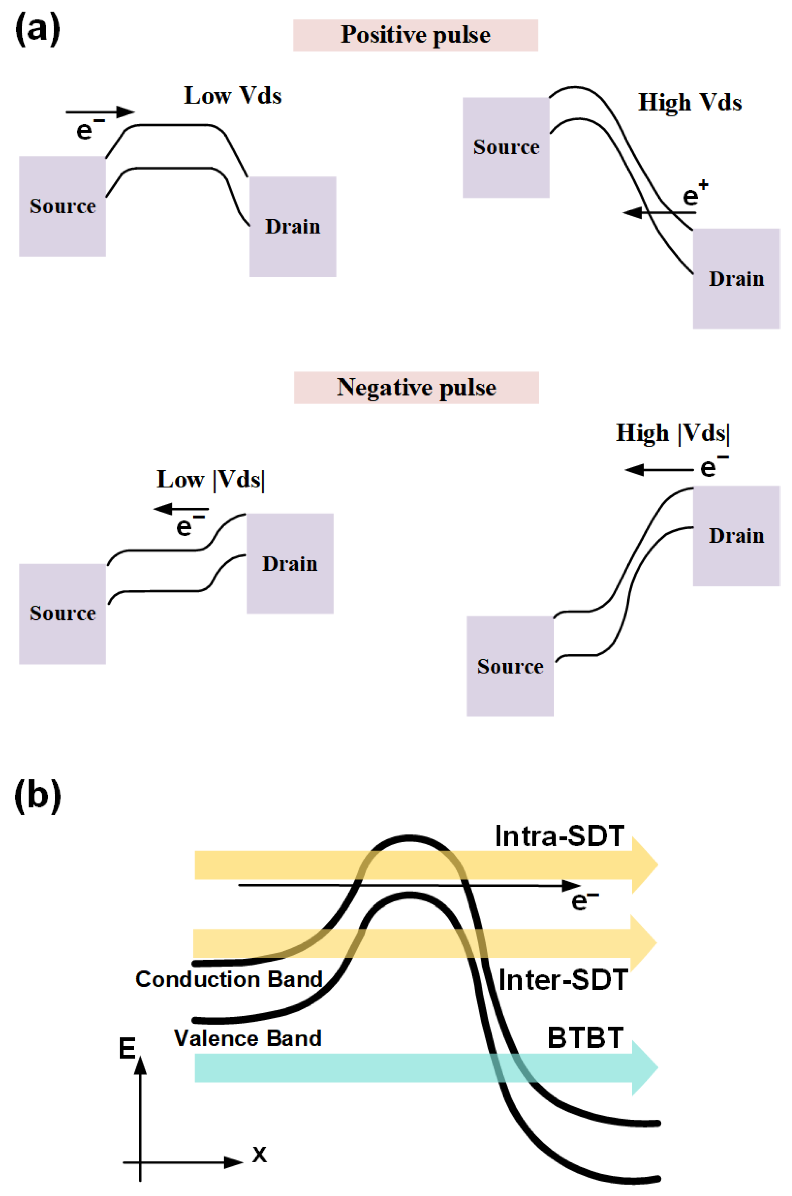
Compared to traditional silicon-based MOSFET devices, the CNTFET, with its unique quasi-one-dimensional nanostructure and superior ballistic transport characteristics, can effectively suppress short-channel effects, providing the possibility for achieving shorter effective gate lengths and faster switching speeds. However, when small-sized CNTFETs are subjected to external transient high voltage impacts, an extremely strong electric field will be formed inside the device, resulting in a significant incline of the band and severe deformation of the potential barrier (as shown in Figure 3).
In this case, the probability of carriers in CNTFET-forming leakage current through a quantum tunneling mechanism will far exceed that of the device at normal operating voltage. Therefore, using only the thermionic current model cannot accurately describe the complex operating behavior of the device under high field strength and high bias conditions, such as ESD. In order to accurately describe the working characteristics and failure mechanism of CNTFET in ESD events, we must accurately model the tunneling leakage current of CNTFET. We divide the leakage current in CNTFET into two categories: Source–Drain Tunneling (SDT) and Band–Band Tunneling (BTBT), as shown in Figure 3.
Source–drain tunneling refers to the leakage current formed by electrons or holes directly penetrating the channel barrier between the source and drain. Due to the quasi one-dimensional channels of carbon nanotubes, the potential barrier shape between the source and drain can be approximated by a simplified trapezoidal/triangular potential barrier. For one-dimensional potential barriers, the transmittance given by the Wentzel–Kramers–Brillouin method (WKB) is generally in the form of [30]:
T ( E ) = exp 2 x 1 x 2 2 m [ Φ ( x ) E ]   d x
Φ ( x ) is the energy distribution of the potential barrier between source and drain, m is the effective mass of the carrier, E is the incident energy level of the particle, and x1 and x2 are the classical inflection points of the tunneling potential barrier. Assuming x1 and x2 are the barrier heights at the source and drain, respectively, when Vds is high, the barrier height linearly decreases from x1 at the source to Φ 2 = Φ 1 q V d s at the drain, which can be approximated as a trapezoidal barrier. Integrating Equation (11) under this linear potential barrier yields an analytical approximation of the tunneling emissivity:
T ( E ) exp 2 2 m * 3 q V d s ( Φ 1 3 / 2 Φ 2 3 / 2 )
When Vds is large enough that Φ 2 approaches 0, the shape of the potential barrier transforms into a triangle, and its transmittance is determined only by the height of the potential barrier at the source. At this point, Equation (12) can be further simplified as
T ( E ) exp 4 2 m * L e f f ( Φ 1 ) 3 / 2 3 q V d s
L e f f is the equivalent barrier width. It can be seen that the tunneling transmittance is exponentially correlated with the barrier height Φ 1 and inversely proportional to Vds. Combine various constants and pre-factors into a fitting parameter A S D T , and we finally obtain a compact model explicit expression for SDT leakage current:
I S D T = A S D T exp B S D T ( Φ b ) β S D T V d s
Φ b represents the height of the potential barrier at the source (which can be estimated by the deviation between gate voltage and threshold voltage, for example, approximately Φ b q ( V t h V g s ) in the subthreshold region), β S D T is the exponential factor of tunneling current on the height of the potential barrier, and B S D T is the fitting coefficient related to material and geometric parameters (reflecting the influence of barrier width, effective mass of the active region, etc., on tunneling probability). A S D T is the current amplitude fitting parameter (reflecting the overall scale of carrier density and transmission probability at the source). Parameters A S D T , B S D T , and β S D T can be extracted by fitting with the I-V characteristics of experiments or numerical simulations. The above model formula is simple in form and can be easily incorporated into the traditional leakage current model dominated by thermionic emission.
In an N-type CNTFET, when a high drain-source voltage is applied, the energy bands of the source and drain may overlap. When the highest energy level of the valence band of the drain (or near the drain region of the channel) exceeds the lowest energy level of the source conduction band, a BTBT current is generated from the drain valence band to the source conduction band. This process is driven by a strong transverse electric field, particularly evident in one-dimensional CNT band structures.
Due to the fact that the bandgap E g of CNT is determined by the tube diameter and does not significantly change with bias voltage, the transverse electric field at high bias voltage causes the barrier width ( Δ x E g / ( q F ) ) to decrease with increasing Vds, where F ( F ( V D S V 0 ) / L e f f ) is the approximate electric field strength, and Leff is the effective barrier length. Therefore, as Vds further increases, the tunneling barrier becomes thinner, the tunneling probability significantly increases, and BTBT current is formed. Under the above approximation, the tunneling probability of electrons (or holes) in a single energy level within the barrier can be approximated by WKB as follows:
I B T B T = A B T B T exp B B T B T ( V D S V 0 ) β B T B T
A B T B T is the front exponential term, which is proportional to CNT diameter and density, carrier effective state density, Fermi velocity, etc. It reflects the available energy and channel cross-sectional area of the conduction and valence band; B B T B T is related to the tunneling barrier characteristics and usually increases with Eg and effective mass. β B T B T is a power exponent, which is related to the shape of the potential barrier and nonlinear effects. For an ideal triangular potential barrier, β B T B T = 1, but in practical devices, β B T B T > 1; V0 is the threshold voltage of BTBT, corresponding to Vds when the conduction band and valence band are perfectly aligned and overlap. Therefore, when Vds < V0, the model is invalid, and I B T B T 0 . When Vds > V0, the current increases exponentially. This formula has a compact structure and can be directly used for circuit simulation, avoiding the WKB integration process. Only parameters such as A B T B T ,   B B T B T ,   β B T B T , V 0 need to be determined through experiments or simulations.
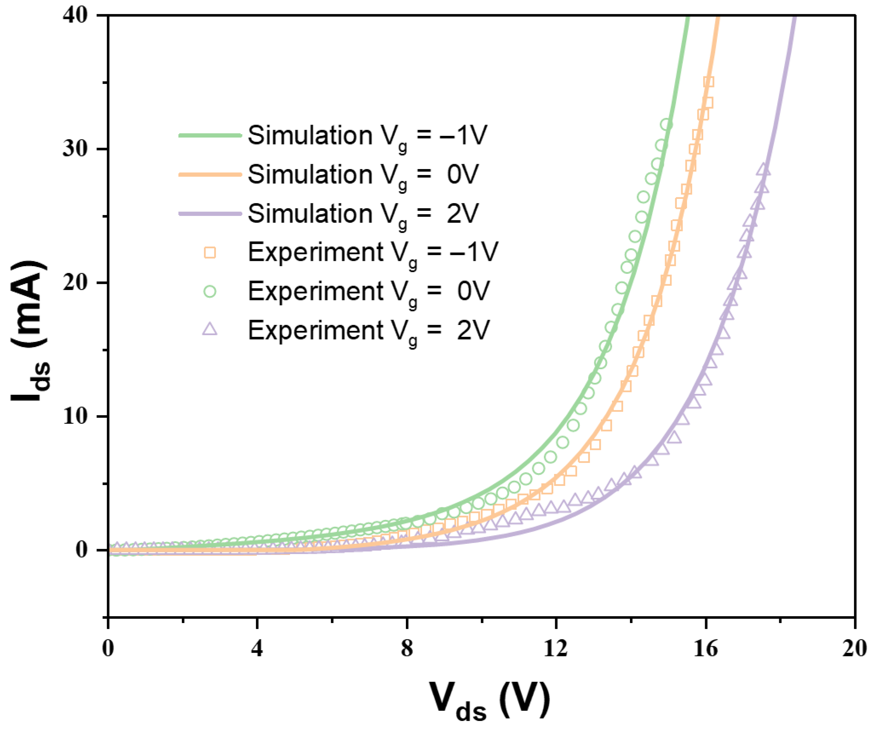
A test is conducted on CNTFET: three gate voltage states, Vg = −1 V, 0 V, and 2 V, are selected, with the source grounded (VSource = 0 V). A stepwise ESD test voltage Vds is applied to the drain, and Ids is recorded at each voltage to obtain the Ids vs. Vds characteristic as shown in Figure 4. To avoid parasitic effects and drift caused by instantaneous overheating, current compliance values and fixed integration times are set during the testing process.
Based on the theoretical model of tunneling current mentioned above, we modeled and numerically simulated the tunneling behavior in the high Vds region under three gate bias conditions consistent with the experiment. The simulation results are shown in solid lines in the same coordinate system. The model, with its main parameter settings summarized in Table 1, starts from the height/thickness of the barrier controlled by the gate voltage, and uniformly describes the reduction in the barrier and the increase in the penetration probability under the increase of Vds; all parameters are calibrated within the same framework and maintain consistency throughout the entire voltage range. As shown in Figure 4, the established model can clearly demonstrate the regulation law and magnitude of gate voltage on tunneling current: in low voltage region, the currents are close to zero; As Vds increases, Ids rapidly increases and shows a clear gating sequence—when Vg = −1 V, the potential barrier decreases and the tunneling probability increases, so Ids is the highest at the same Vds; Vg = 0 V, followed by the positive gate bias Vg = 2 V, which raises the potential barrier, suppresses tunneling, and minimizes Ids. The overall agreement between the model and the measured data is good, and it can simultaneously reproduce the exponential rise pattern of the experiment and the relative relationship between the three gate voltages. The slight deviation at the high voltage may be related to self-heating, field dependence of contact barriers, or series resistance. The above results verify the model’s ability to describe the tunneling conductivity of CNTFET under ESD conditions, providing a reliable basis for subsequent reliability evaluation and circuit-level simulation.
Table 1. Model parameter definitions and values.
ParameterDescriptionValue
W ( μ m ) Gate width30
L ( μ m ) Gate length4
E g ( e V ) CNT bandgap0.75
A q c ( f F / μ m ) Quantum-capacitance effective coefficient0.087
B q c ( f F / μ m ) Quantum-capacitance offset0.150
V t ( V ) Threshold voltage0.42
δ DIBL coefficient0.02
n s s Subthreshold slope factor1.15
λ e f f ( n m ) Equivalent mean free path90
μ ( c m 2 / ( V s ) ) Low field effective mobility1.31 × 102
β Fitting parameters1.73
Φ b ( e V ) Height of potential barrier at source0.28
A S D T SDT pre-exponential amplitude3.0 × 10−13
B S D T SDT exponential slope factor33.6
β S D T Fitting parameters1.10
A B T B T BTBT pre-exponential amplitude2.0 × 10−13
B B T B T BTBT exponential slope factor7.1 × 108
β B T B T Fitting parameters1.25
V 0 ( V ) BTBT threshold voltage5

2.3. Thermal Breakdown

In ESD events, the transient high current experienced by CNTFET devices can lead to significant Joule heating effects. When the power consumption of the device exceeds its thermal tolerance limit, the CNTFET will undergo irreversible thermal damage, ultimately leading to permanent failure. In order to accurately describe this critical failure mechanism in a compact model, this paper constructs a specialized thermal breakdown module. According to Duan et al.’s study [13], the failure process of CNTFET under ESD stress exhibits a clear three-stage characteristic, with thermal failure being the dominant mechanism for the final failure of the device. When the instantaneous power consumption of the device exceeds the critical threshold P0, the temperature inside the carbon nanotube channel rises sharply, causing C-C bond breakage and channel damage, and the device transitions from a conductive state to a high-resistance state.
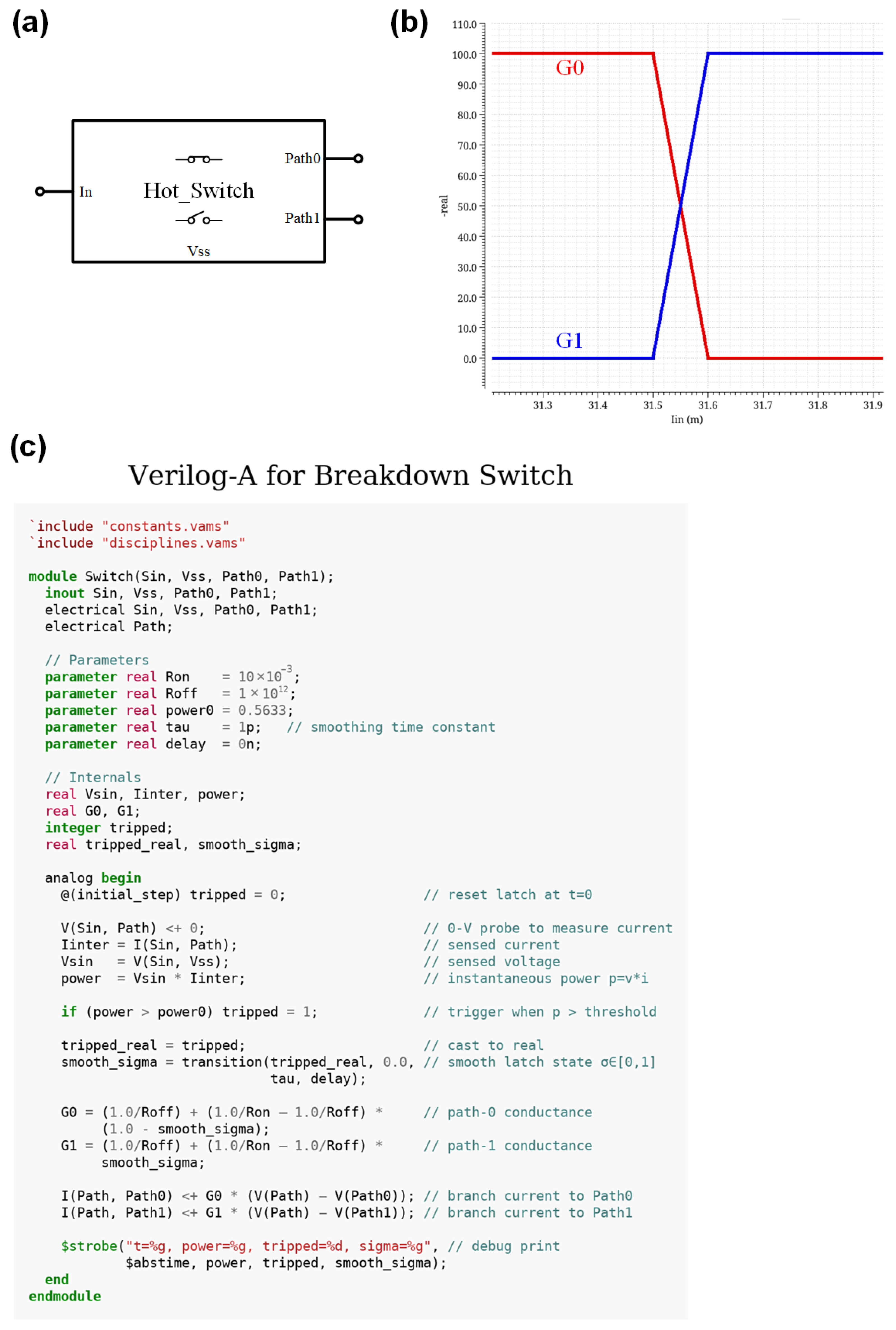
The hot-switch behavioral module judges based on the power consumption and the set threshold. When the instantaneous power consumption exceeds the preset threshold power0, the device quickly transitions from a conducting state to a high-resistance state and introduces a parallel low resistance breakdown path to simulate the thermal breakdown phenomenon; see Figure 5.
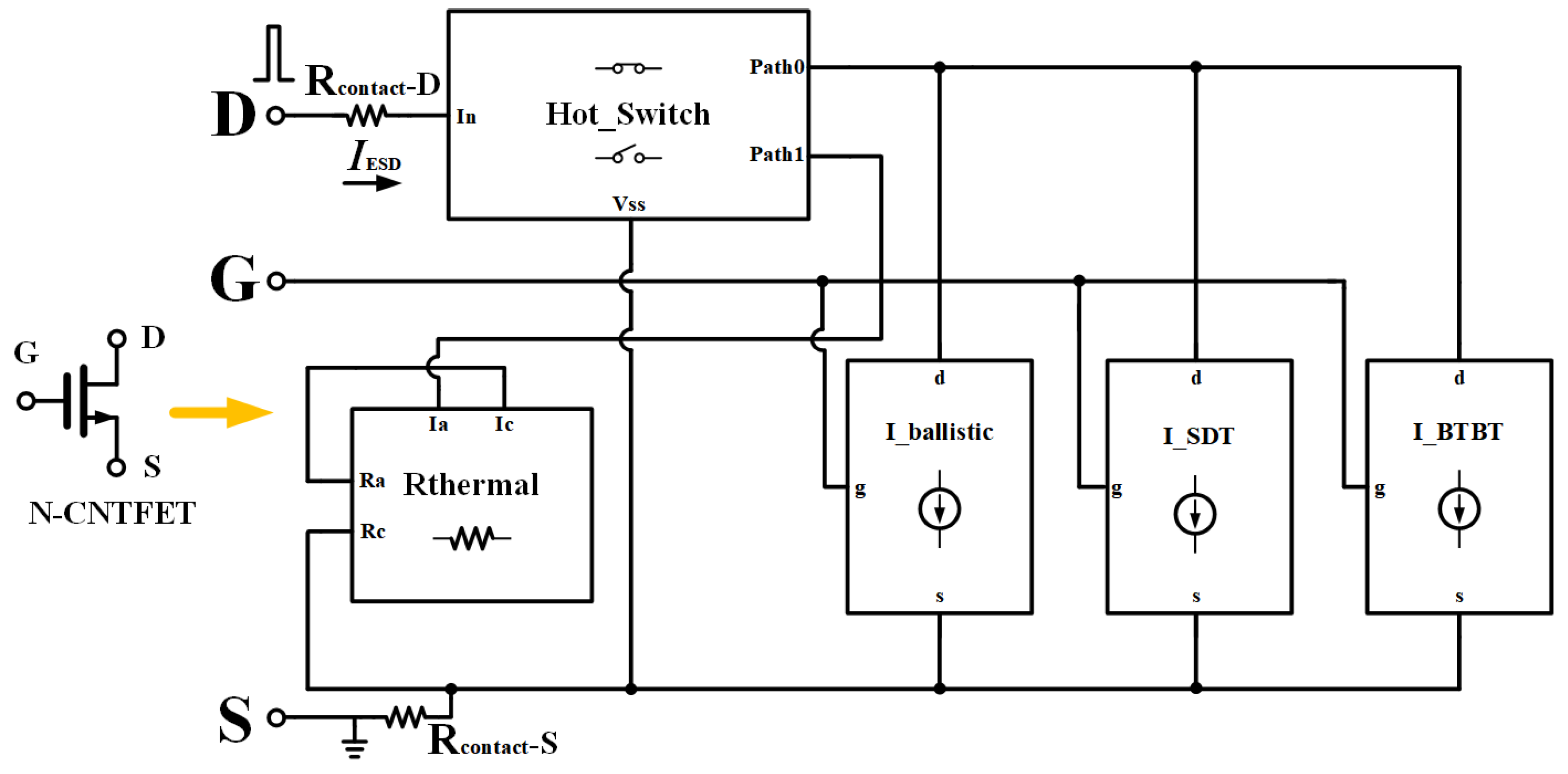
From electrical measurements at the breakdown point during ESD testing of the LBG-CNTFET, we extract the resistance. By incorporating the Rthermal module into the aforementioned model, we simulate the low-resistance path formed after device breakdown. The proposed ESD hybrid model of CNTFET is shown in Figure 6.
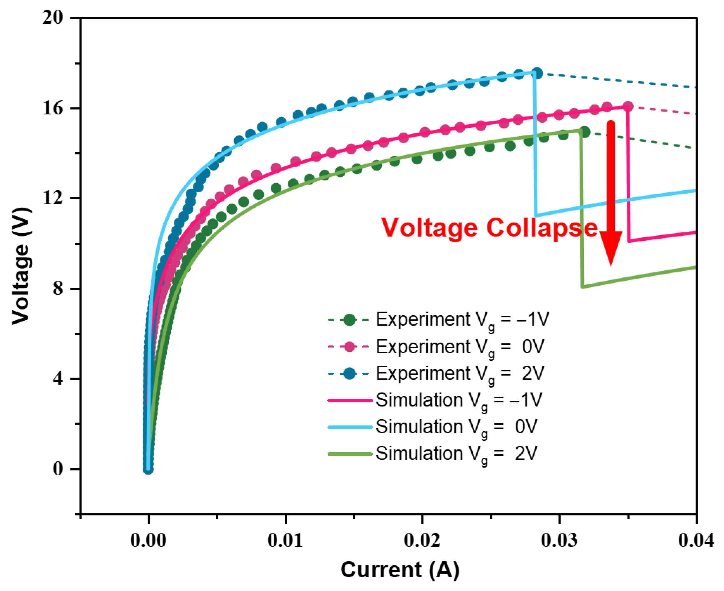
We use DC scanning current to simulate the current model established earlier by adding a thermal breakdown switch. The simulation results are shown in Figure 7. The points are test data, and the three curves represent simulation data corresponding to simulation results under different gate voltages. When the power consumption of the circuit approaches the test value, the thermal breakdown switch is quickly triggered, instantly setting the original current path to a high resistance path and connecting a low resistance path in parallel to simulate the thermal breakdown process. From the simulation results, it can be seen that as the power consumption reaches the critical value, the current path undergoes significant changes, reflecting the failure process of CNTFET devices caused by thermal effects under ESD events. Especially when the power consumption exceeds the threshold, the voltage of the device drops sharply, exhibiting a hysteresis-like characteristic, which is consistent with the phenomenon observed in actual testing. By comparing simulation and test data, the effectiveness and accuracy of the established model in describing the thermal breakdown process of CNTFET can be verified.
Overall, our model is compact and data-calibrated, so it can cover the full bias window needed for device sweeps and ESD co-simulation without resorting to Non-Equilibrium Green’s Function (NEGF). In thermionic current, we use a Landauer/virtual-source core: current is written at a virtual source with an inversion-charge term, contact/series resistances are de-embedded at the terminals, and a smooth transition links linear and velocity-limited behavior. In tunneling current, we add explicit high-field leakage using WKB-type SDT and BTBT expressions; the onset voltage is tied to drain-side band overlap, and the fitted parameter captures the gate control that enables or suppresses BTBT in LBG CNFET. For thermal breakdown, the electrical core is coupled to a behavioral hot-switch that triggers once a calibrated power threshold is reached.
However, this compact approach has limits: simplified tunneling barriers may miss detailed phonon-assisted pathways far from the fitted window, and the behavioral thermal switch compresses spatially non-uniform heating and stochastic damage into a single power/energy threshold, so it cannot perfectly capture device-to-device variability, duty-cycle effects, or multi-pulse endurance seen in CNT breakdown studies; ultra-short (<1 ns) or long DC stresses may require full transient electro-thermal or NEGF-based analysis.

3. Hybrid Model HBM Test

On the basis of DC simulation, in order to obtain the operating behavior of the established CNTFET hybrid model under real ESD events, we built an HBM equivalent test circuit using the ideal cell library in Cadence Virtuoso to simulate the occurrence of HBM events, as shown in Figure 8.
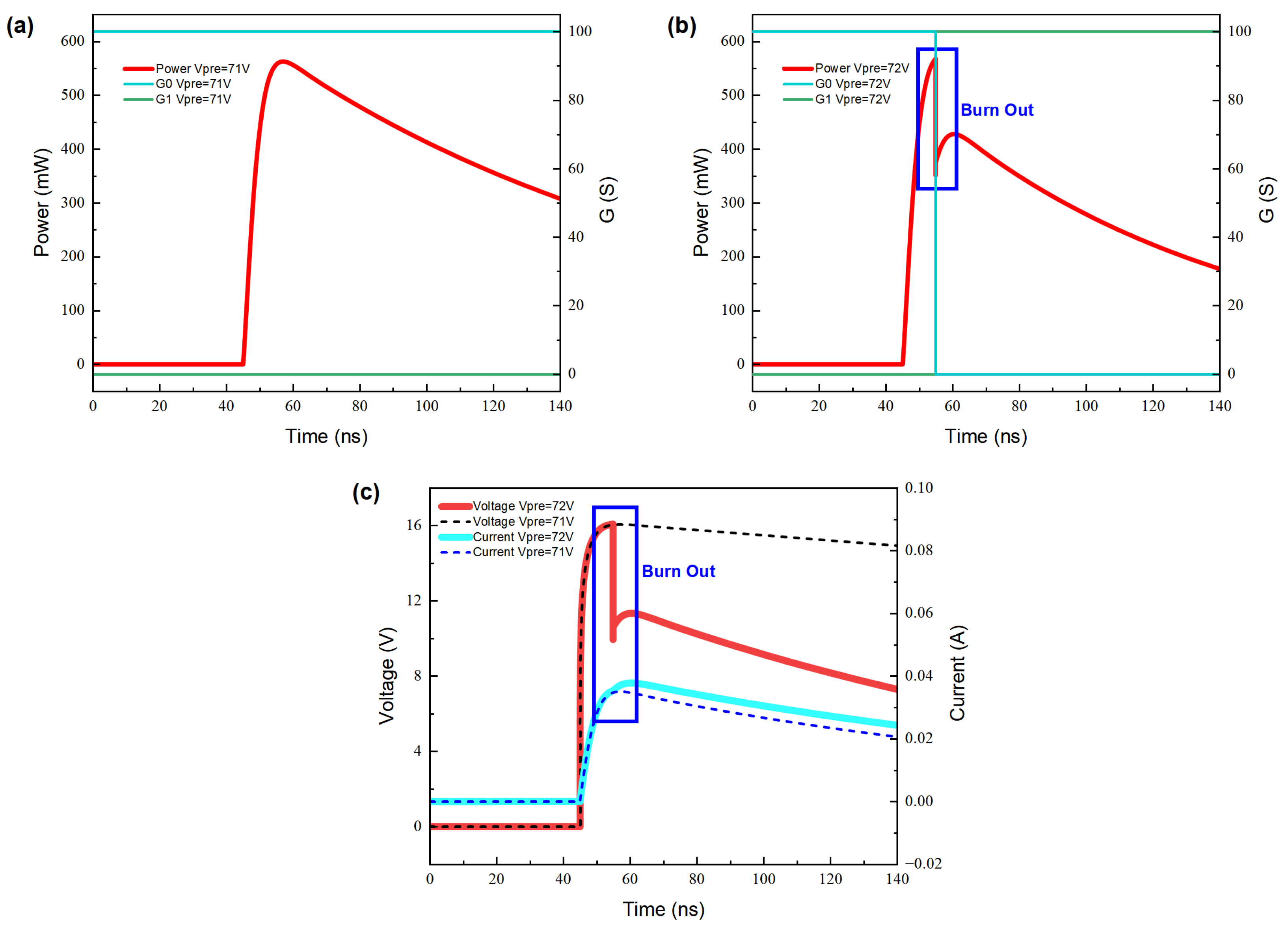
The ESD model is tested by gradually increasing the HBM pre-charge voltage Vpre, and the simulation results are shown in Figure 9. Figure 9a,c show that when Vpre is less than or equal to 71 V, the power consumption of the device will not exceed the measured value power0, and the device can withstand the ESD voltage. In this state, the CNTFET mainly discharges ESD energy through tunneling current. Figure 9b shows that when Vpre reaches 72 V, the power consumption will exceed power0, and the thermal breakdown switch will be triggered; At the next moment, the power consumption of the device drops sharply. From Figure 9c, it can be seen that at the moment of breakdown, the drain voltage of the CNTFET drops sharply from 16.04 V to 9.92 V, indicating that the resistance switching of the thermal breakdown switch is successfully achieved. The breakdown path in the device is successfully introduced, and the original discharge path is set to a high-resistance state and no longer participates in current discharge.
In Table 2, we compare the conduction and breakdown mechanisms captured by classical silicon-based ESD models and by our proposed LBG-CNTFET ESD model. The CNT-based model retains the baseline thermionic emission mode and also explicitly includes both SDT and BTBT conduction, recognizing that under high ESD stress, these tunneling paths become significant in narrow-gap carbon channels. Different from silicon devices, our model excludes any parasitic BJT conduction path, since the CNT channel architecture lacks the physical PN-junction substrate coupling needed to form a BJT. As with silicon ESD models, we also incorporate a thermal-triggered low-resistance switching behavior to represent the post-breakdown conduction path. By calibrating the model parameters to match measured ESD threshold and current behavior, we ensure that the model is not only physically comprehensive but also quantitatively meaningful in capturing observed ESD performance. Hence, this comparative presentation validates both the physical completeness and the practical relevance of our LBG-CNTFET ESD model.

4. Conclusions

Based on the test and parameter extraction results of LBG-CNTFET, this study investigates, in detail, the mechanism of excitation current for hot carriers and tunneling current, and fully describes the current behavior of CNTFET. Finally, a complete CNTFET ESD model is constructed. By introducing a thermal breakdown switch module, this model can effectively simulate the thermal breakdown mechanism of CNTFET under extreme ESD conditions, demonstrating strong adaptability and accuracy.
In both the DC simulation and the HBM equivalent test, the proposed model can well describe the working state of CNTFET, especially in simulating the thermal breakdown failure process. The model can predict the power consumption changes and current path switching in real time under ultra-high voltage conditions, achieving dynamic response simulation under ESD events. The simulation results show that the ESD model can withstand an HBM test voltage of Vpre = 72 V. In addition, the comparison between experimental results and simulation data validates the high fitting of the model under different gate voltages, further demonstrating the effectiveness and reliability of the model in complex ESD environments.
Future work should focus on expanding the model to incorporate multi-tube CNTFETs, enhancing its scalability, and application in more complex integrated circuits. Additionally, exploring the impact of other novel carbon-based materials and further improving the model’s robustness under extreme conditions could pave the way for the next generation of carbon nanotube-based electronics.
Through the optimization and verification of this study, it not only provides new ideas for the ESD protection design of CNTFETs but also lays the foundation for the development of standard cells and I/O libraries for carbon-based electronic devices.

Author Contributions

Conceptualization, W.Z. and C.C.; software simulation and parameter optimization, W.Z., Y.Z., Q.G. and C.C.; data processing, W.Z., X.X., Y.G. and Z.C.; writing—original draft preparation, W.Z.; writing—review and editing, C.C. and J.J.; supervision, C.C. and J.J. All authors have read and agreed to the published version of the manuscript.

Funding

This research was funded by the Natural Science Foundation of Fujian Province (2023H0052), the Major science and technology projects of Xiamen (3502Z20221022), the National Natural Science Foundation of China (6247011759), and the Project of the Central Guided Local Science and Technology Development Fund: Research on multi-stage Intelligent Fire Detection and Monitoring of Li-ion Battery Energy Storage Systems (246Z4404G).

Institutional Review Board Statement

Not applicable.

Informed Consent Statement

Not applicable.

Data Availability Statement

The original contributions presented in this study are included in the article. Further inquiries can be directed to the corresponding author.

Conflicts of Interest

The author, Ying Gao, is an employee of Jade Bird Fire Co., Ltd. The author declares no conflicts of interest. The funders had no role in the design of the study; in the collection, analyses, or interpretation of data; in the writing of the manuscript; or in the decision to publish the results.

References

  1. Zahoor, F.; Hanif, M.; Bature, U.I.; Bodapati, S.; Chattopadhyay, A.; Hussin, F.A.; Abbas, H.; Merchant, F.; Bashir, F. Carbon nanotube field effect transistors: An overview of device structure, modeling, fabrication and applications. Phys. Scr. 2023, 98, 082003. [Google Scholar] [CrossRef]
  2. Gupta, N.; Dixit, A. Carbon Nanotube Field-Effect Transistors (CNFETs): Structure, Fabrication, Modeling, and Performance. In Carbon Nanomaterial Electronics: Devices and Applications; Hazra, A., Goswami, R., Eds.; Advances in Sustainability Science and Technology; Springer: Singapore, 2021. [Google Scholar] [CrossRef]
  3. Chen, Z.; Chen, J.; Liao, W.; Zhao, Y.; Jiang, J.; Chen, C. Progress on a Carbon Nanotube Field-Effect Transistor Integrated Circuit: State of the Art, Challenges, and Evolution. Micromachines 2024, 15, 817. [Google Scholar] [CrossRef] [PubMed]
  4. Franklin, A.D.; Luisier, M.; Han, S.-J.; Tulevski, G.; Breslin, C.M.; Gignac, L.; Lundstrom, M.S.; Haensch, W. Sub-10 nm carbon nanotube transistor. Nano Lett. 2012, 12, 758–762. [Google Scholar] [CrossRef] [PubMed]
  5. Maqbool, M.; Sharma, V.K. Review of carbon nanotube field effect transistor for nanoscale regime. Curr. Nanosci. 2023, 20, 459–470. [Google Scholar] [CrossRef]
  6. Sanju, I.M.S.; Vadivel, M.; Mathan, N. Performance evaluation of an efficient dual stage compressor using 32 nm CNTFET technology for high speed and low power digital applications. J. Nanoelectron. Optoelectron. 2024, 19, 1259–1268. [Google Scholar] [CrossRef]
  7. Yao, X.; Zhang, Y.; Jin, W.; Hu, Y.; Cui, Y. Carbon Nanotube Field-Effect Transistor-Based Chemical and Biological Sensors. Sensors 2021, 21, 995. [Google Scholar] [CrossRef]
  8. Liu, H.-Y.; Sun, Y.; Sun, D.-M.; Cheng, H.-M. Carbon Nanotube 3D Integrated Circuits: From Design to Applications. Adv. Funct. Mater. 2025, 35, 2424012. [Google Scholar] [CrossRef]
  9. Bishop, M.D.; Hills, G.; Srimani, T.; Lau, C.; Murphy, D.; Fuller, S.; Humes, J.; Ratkovich, A.; Nelson, M.; Shulaker, M.M. Fabrication of carbon nanotube field-effect transistors in commercial silicon manufacturing facilities. Nat. Electron. 2020, 3, 492–501. [Google Scholar] [CrossRef]
  10. Tagliaferri, A.; Shkodra, B.; Costa Angeli, M.A.; Ploner, M.; Petrelli, M.; Altana, A.; Ibba, P.; Lugli, P.; Petti, L. Stability and Functionalization of Carbon Nanotube Electrolyte-Gated Field-Effect Transistors. In Proceedings of SIE 2024; Valle, M., Gastaldo, P., Limiti, E., Eds.; Lecture Notes in Electrical Engineering; Springer: Cham, Switzerland, 2025; Volume 1263. [Google Scholar] [CrossRef]
  11. Yao, Z.; Kane, C.L.; Dekker, C. High-field electrical transport in single-wall carbon nanotubes. Phys. Rev. Lett. 2000, 84, 2941–2944. [Google Scholar] [CrossRef]
  12. Shrivastava, M.; Kulshrestha, N.; Gossner, H. ESD Investigations of Multiwalled Carbon Nanotubes. IEEE Trans. Device Mater. Reliab. 2014, 14, 555–563. [Google Scholar] [CrossRef]
  13. Duan, Y.; Yang, C.; Zhang, D.; Gao, Y.; Sun, Y.; Si, J.; Lu, P.; Li, X.; Bu, J.; Li, B. Electrostatic Discharge and Failure Model of Carbon Nanotube Field-Effect Transistors. IEEE Trans. Electron Devices 2025, 72, 1617–1623. [Google Scholar] [CrossRef]
  14. Pan, Z.; Li, X.; Hao, W.; Miao, R.; Wang, A. On-chip ESD Protection Design Methodologies by CAD Simulation. ACM Trans. Des. Autom. Electron. Syst. 2023, 29, 4. [Google Scholar] [CrossRef]
  15. Lu, F.; Ma, R.; Dong, Z.; Wang, L.; Zhang, C.; Wang, C.; Chen, Q.; Wang, X.S.; Zhang, F.; Li, C.; et al. A Systematic Study of ESD Protection Co-Design With High-Speed and High-Frequency ICs in 28 nm CMOS. IEEE Trans. Circuits Syst. I Regul. Pap. 2016, 63, 1746–1757. [Google Scholar] [CrossRef]
  16. Li, J.; Joshi, S.; Barnes, R.; Rosenbaum, E. Compact modeling of on-chip ESD protection devices using Verilog-A. IEEE Trans. Comput.-Aided Des. Integr. Circuits Syst. 2006, 25, 1047–1063. [Google Scholar] [CrossRef]
  17. Jiao, C.; Yu, Z. A novel GGNMOS macro-model for ESD circuit simulation. Chin. J. Electron. 2009, 18, 630–634. [Google Scholar]
  18. Hao, W.; Pan, Z.; Li, X.; Miao, R.; Yue, Z.; Wang, A. On-Chip ESD Protection: Design Innovation. IEEE Electron Devices Rev. 2025, 2, 32–51. [Google Scholar] [CrossRef]
  19. Nguyen, H.-N.; Querlioz, D.; Galdin-Retailleau, S.; Dollfus, P. Semiclassical and Quantum Transport in CNTFETs Using Monte Carlo Simulation. IEEE Trans. Electron Devices 2011, 58, 798–804. [Google Scholar] [CrossRef]
  20. Wei, L.; Frank, D.J.; Chang, L.; Wong, H.-S.P. Noniterative Compact Modeling for Intrinsic Carbon-Nanotube FETs: Quantum Capacitance and Ballistic Transport. IEEE Trans. Electron Devices 2011, 58, 2456–2465. [Google Scholar] [CrossRef]
  21. Lee, C.S.; Pop, E.; Franklin, A.D.; Haensch, W.; Wong, H.S.P. A compact virtual-source model for carbon nanotube FETs in the sub-10-nm regime—Part I: Intrinsic elements. IEEE Trans. Electron Devices 2015, 62, 3061–3069. [Google Scholar] [CrossRef]
  22. Lee, C.S.; Pop, E.; Franklin, A.D.; Haensch, W.; Wong, H.S.P. A compact virtual-source model for carbon nanotube FETs in the sub-10-nm regime—Part II: Extrinsic elements, performance assessment, and design optimization. IEEE Trans. Electron Devices 2015, 62, 3070–3077. [Google Scholar] [CrossRef]
  23. Huang, W.; Chen, L. A Compact Model of Carbon Nanotube Field-Effect Transistors for Various Sizes with Bipolar Characteristics. Electronics 2024, 13, 1355. [Google Scholar] [CrossRef]
  24. Chen, Z.; Zhang, Y.; Jiang, J.; Chen, C. An Improved Dual-Gate Compact Model for Carbon Nanotube Field Effect Transistors with a Back-Gate Effect and Circuit Implementation. Electronics 2024, 13, 620. [Google Scholar] [CrossRef]
  25. Avouris, P.; Chen, J. Nanotube electronics and optoelectronics. Mater. Today 2006, 9, 46–54. [Google Scholar] [CrossRef]
  26. Fuad, M.H.; Nayan, M.F.; Noor, S.S.; Yeassin, R.; Mahmud, R.R. Comprehensive performance analysis of CMOS and CNTFET based 8T SRAM cell. J. Electron. Sci. Technol. 2025, 23, 100306. [Google Scholar] [CrossRef]
  27. Zhang, Z.; Zhang, N.; Zhang, Z. High-Performance Carbon Nanotube Electronic Devices: Progress and Challenges. Micromachines 2025, 16, 554. [Google Scholar] [CrossRef]
  28. Datta, S. Quantum Transport: Atom to Transistor; Cambridge University Press: Cambridge, UK, 2005; ISBN 978-0-521-63145-7. [Google Scholar]
  29. Claus, M. Modeling of Ballistic Carbon Nanotube Transistors for Analog High-Frequency Applications. Ph.D. Dissertation, Technische Universität Dresden, Dresden, Germany, 2011. ISBN 978-3942710237. [Google Scholar]
  30. Luisier, M.; Klimeck, G. Modeling direct inter-band tunneling II: Lower-dimensional nanoelectronic devices. J. Appl. Phys. 2014, 116, 054509. [Google Scholar] [CrossRef]
Figure 1. The LBG-CNTFET structure and equivalent circuit model.
Electronicmat 06 00017 g001
Figure 2. The current characteristics dominated by ballistic transport.
Electronicmat 06 00017 g002
Figure 3. (a) Energy band inclination and potential barrier deformation of the CNTFET under different drain–source voltages. (b) Illustration of tunneling current mechanisms in CNTFET, including intra-SDT, inter-SDT, and BTBT processes.
Electronicmat 06 00017 g003
Figure 4. Ids versus Vds under different gate voltages considering IBTBT.
Electronicmat 06 00017 g004
Figure 5. Verilog-A description of a thermal breakdown failure switch. (a) Symbol of the Hot_Switch with input, Vss, Path0 (pre-failure), and Path1 (post-failure). (b) As the input current increases, G0 (Path0) decreases and G1 (Path1) increases once the power threshold is reached (burn-out). (c) Verilog-A hot-switch module used in our simulations (behavioral electro-thermal switch).
Electronicmat 06 00017 g005
Figure 6. ESD hybrid model of CNTFET.
Electronicmat 06 00017 g006
Figure 7. Simulation result versus measured result of thermal breakdown under TLP testing. (The solid lines represent the simulated results obtained from the proposed LBG-CNTFET ESD model, while the dashed lines indicate the post-failure behavior of the device after thermal breakdown, showing the degradation trend observed in the TLP measurements.).
Electronicmat 06 00017 g007
Figure 8. HBM-equivalent test circuit used for ESD co-simulation: C1 = 150 pF, R1 = 1.5 kΩ, L1 = 7.5 μH, C2 = 1 pF. Pre-charge: SW1 closed/SW2 open; after charge: SW1 open; at t = 45 ns, SW2 closes to apply the HBM pulse (ESD) to the LBG-CNTFET. The red part represents the LBG-CNTFET ESD model established in this work.
Electronicmat 06 00017 g008
Figure 9. Simulation results of the HBM test circuit (G0 and G1 denote the conductance of Path0 and Path1 in the behavioral hot-switch module). (a) With HBM pre-charge Vpre = 71 V, the device remains intact: G0 stays high, G1 remains off, and the CNTFET power exhibits a single peak without triggering the thermal switch. (b) With HBM pre-charge Vpre = 72 V, the power transient crosses the calibrated threshold; the switch latches to the failure branch (blue “Burn-Out” window), G0 drops, and G1 turns on, indicating the formation of a post-failure low-resistance path. (c) Comparison of drain voltage and current at Vpre = 71 V and 72 V shows voltage collapse accompanied by a current surge after burnout, whereas the 71 V case does not latch into failure.
Electronicmat 06 00017 g009
Table 2. Comparative summary of conduction and breakdown mechanisms in silicon-based ESD models vs. the proposed LBG-CNTFET ESD model.
MechanismSilicon-Based ESD Model [16,17]LBG-CNTFET ESD ModelImplication
Thermionic emissionModeledModeledCarrier injection over the barrier dominates under normal bias conditions.
High voltage: SDTMinorSignificantIn very short-channel CNT channels under high field, SDT becomes non-negligible.
High voltage: BTBTMinorSignificantCNT channel with narrower effective gaps allows stronger BTBT under ESD stress.
Parasitic BJT conductionYesNoIn the CNT-based device structure, the parasitic BJT path does not exist
After breakdown: switch to low-resistance pathModeledModeledBoth models include a low-resistance path
ESD trigger thresholdModeledModeledThe threshold is a key figure of merit for the ESD model
Disclaimer/Publisher’s Note: The statements, opinions and data contained in all publications are solely those of the individual author(s) and contributor(s) and not of MDPI and/or the editor(s). MDPI and/or the editor(s) disclaim responsibility for any injury to people or property resulting from any ideas, methods, instructions or products referred to in the content.