
Progress in Hexagonal Boron Nitride (h-BN)-Based Solid-State Neutron Detector


Abstract
:1. Introduction
2. Materials and Methods
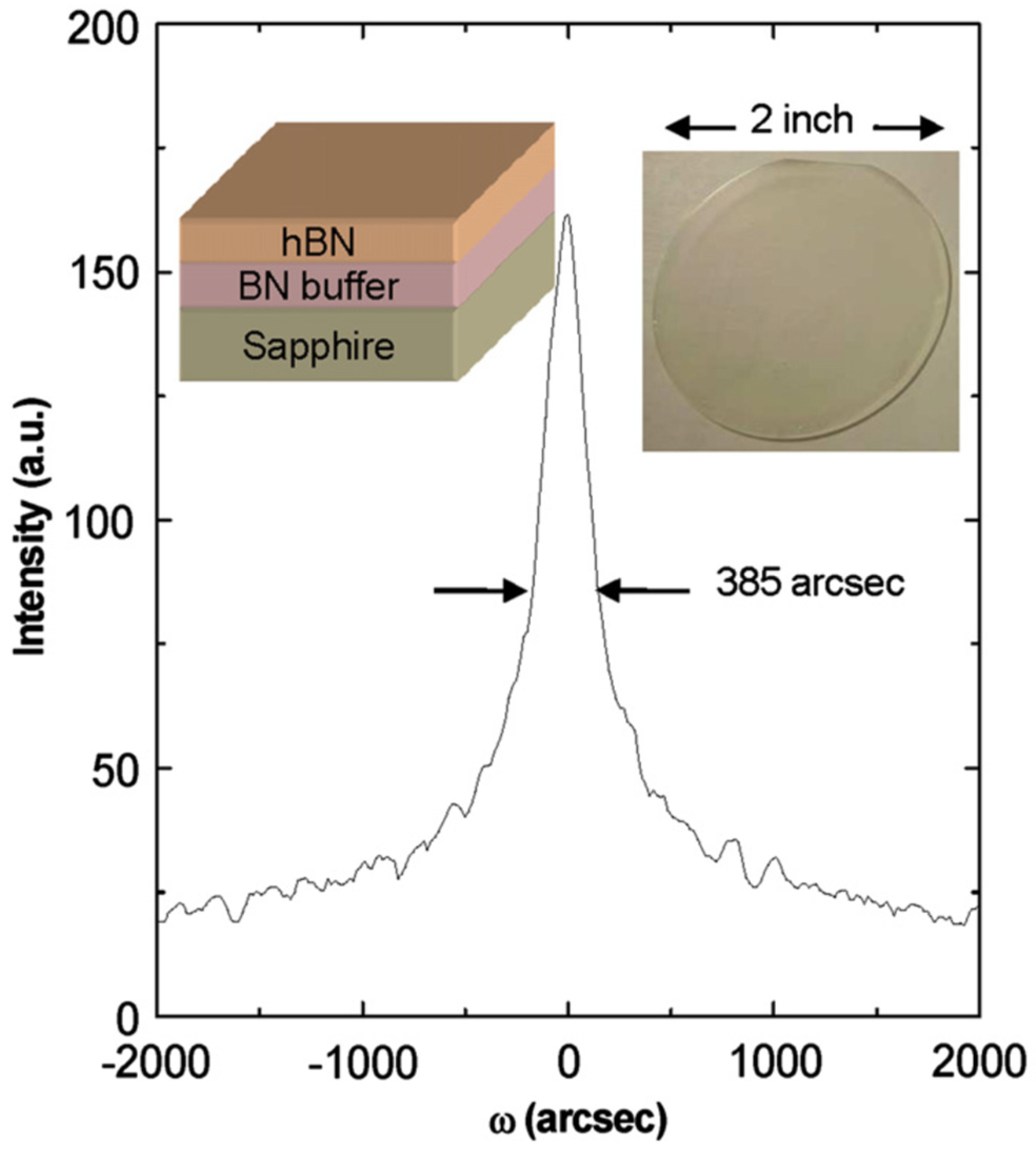
2.1. Growth of h-BN
2.2. h-BN Device Fabrication Processes
2.2.1. Etching
2.2.2. Ohmic Contacts
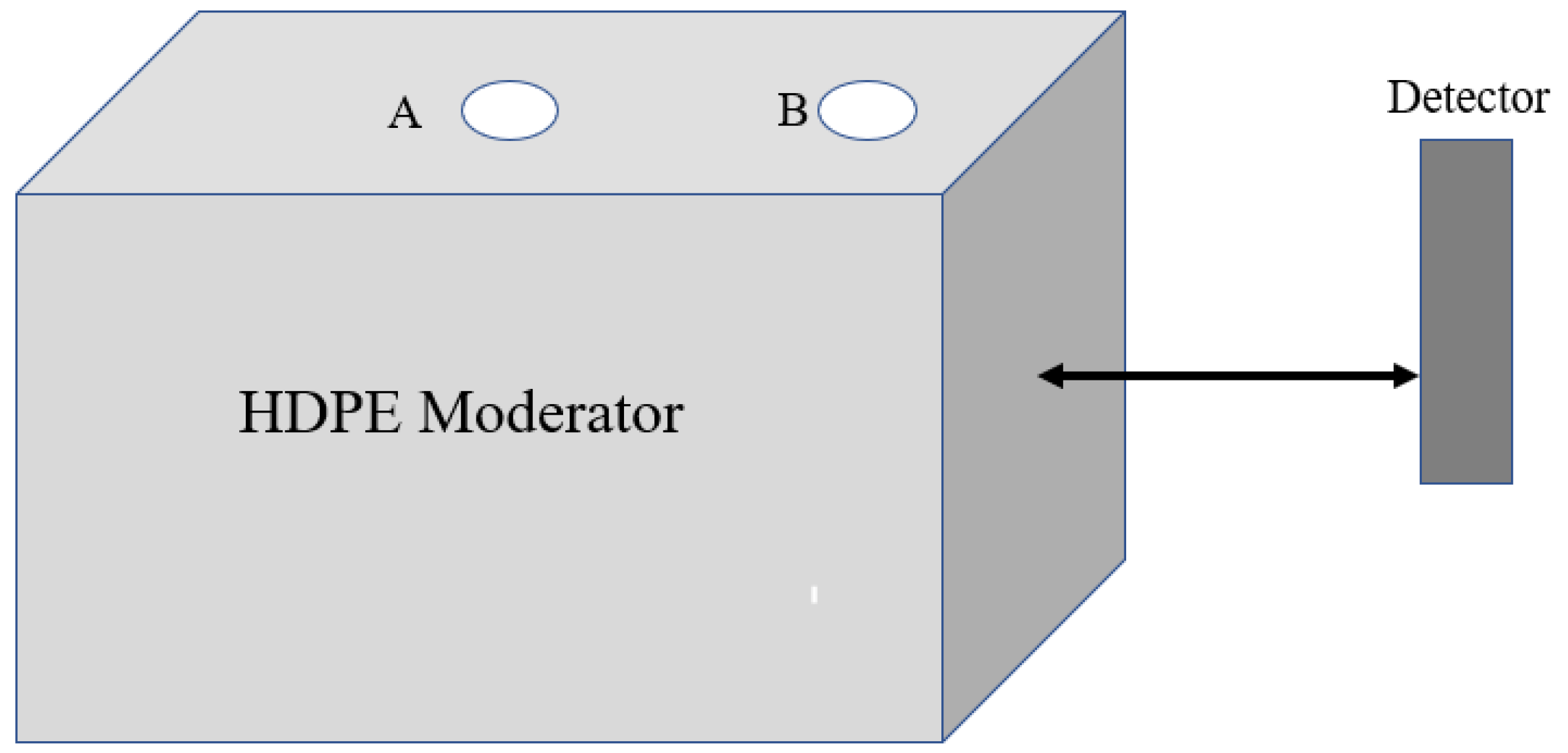
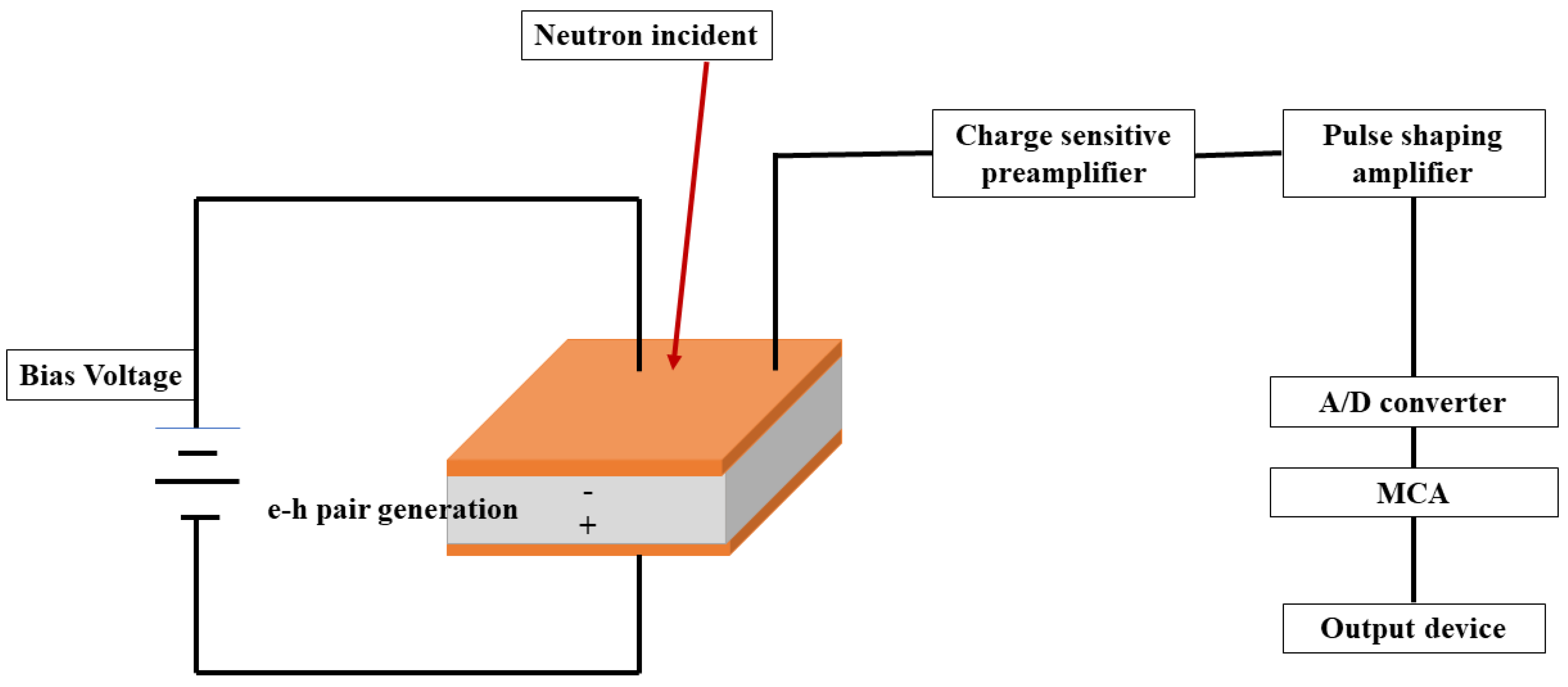
2.3. Experimental Setup
3. Results and Discussions
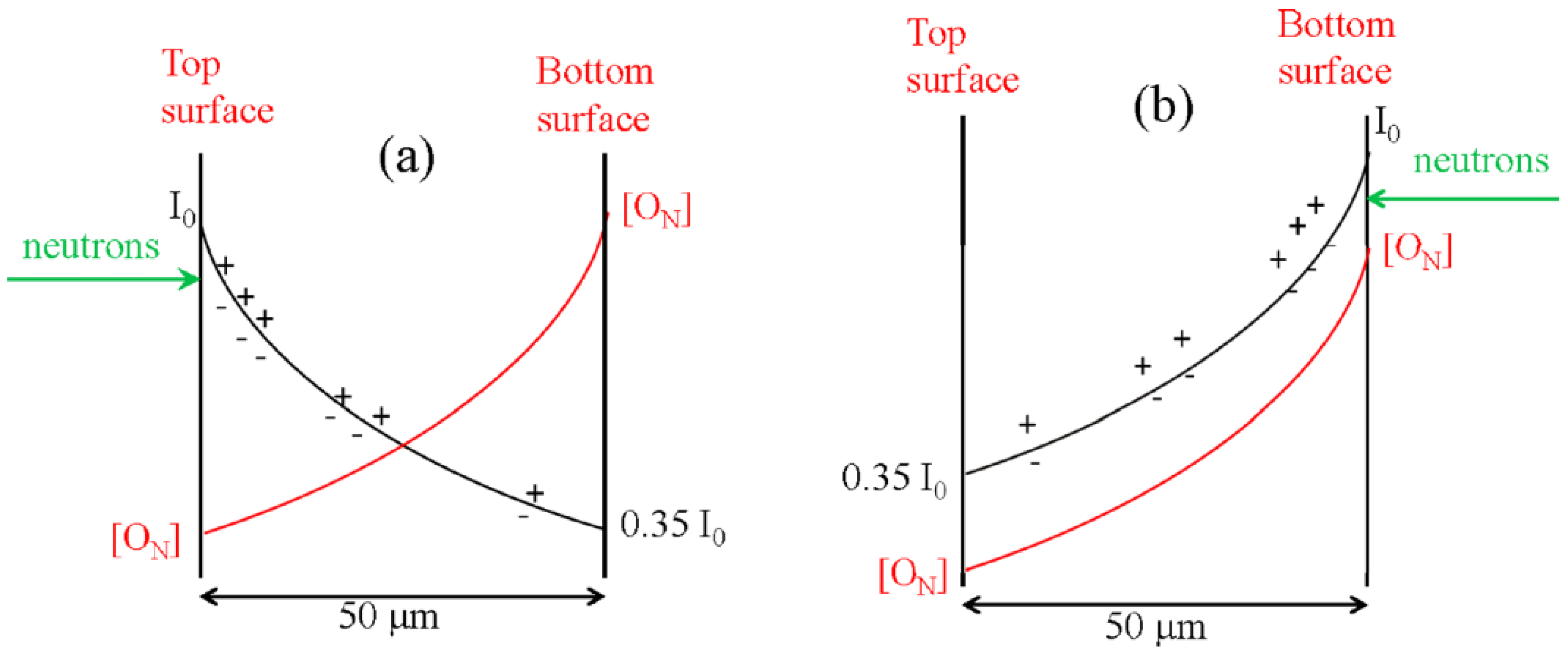
3.1. Point Defect Issues
3.2. Ohmic Contacts
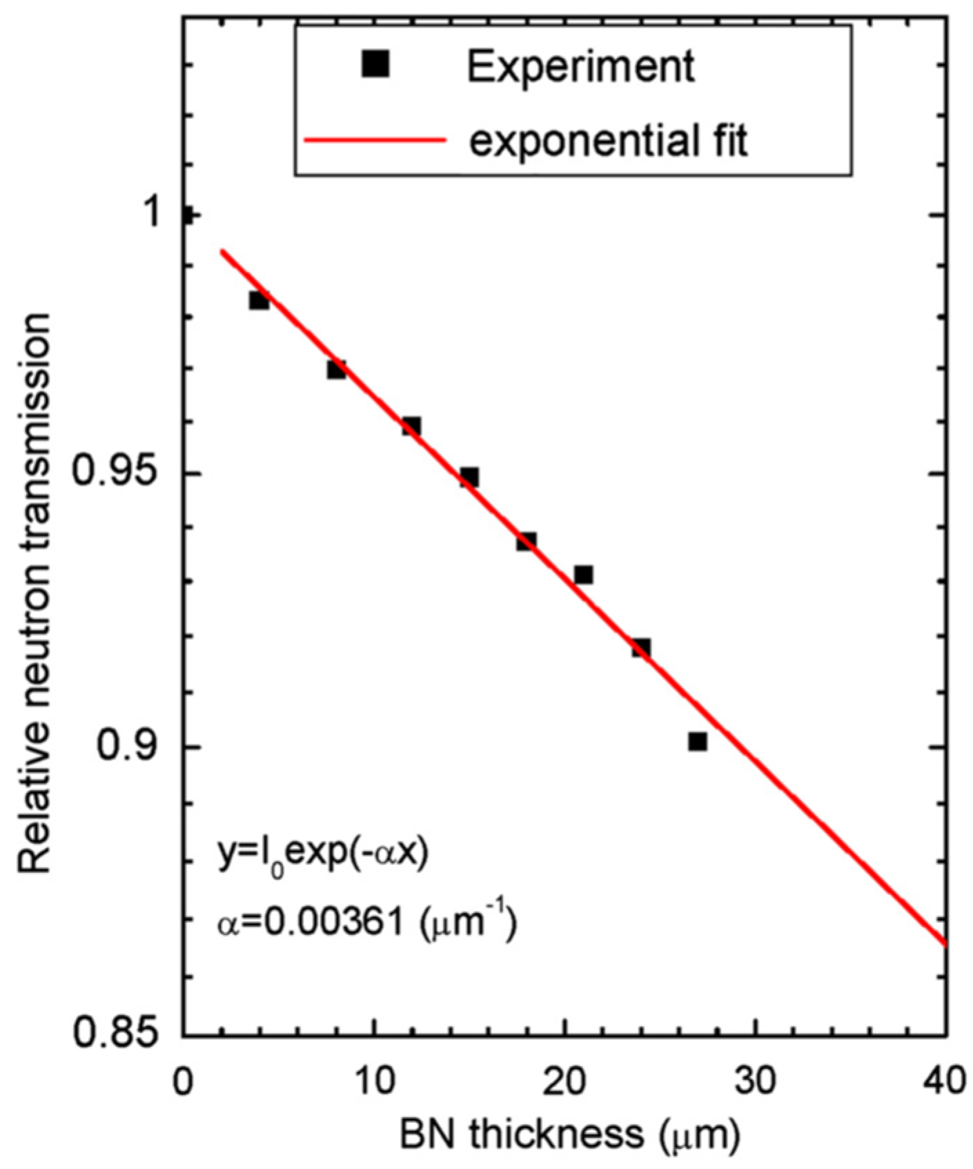
3.3. Epilayer Thickness and Absorption Length
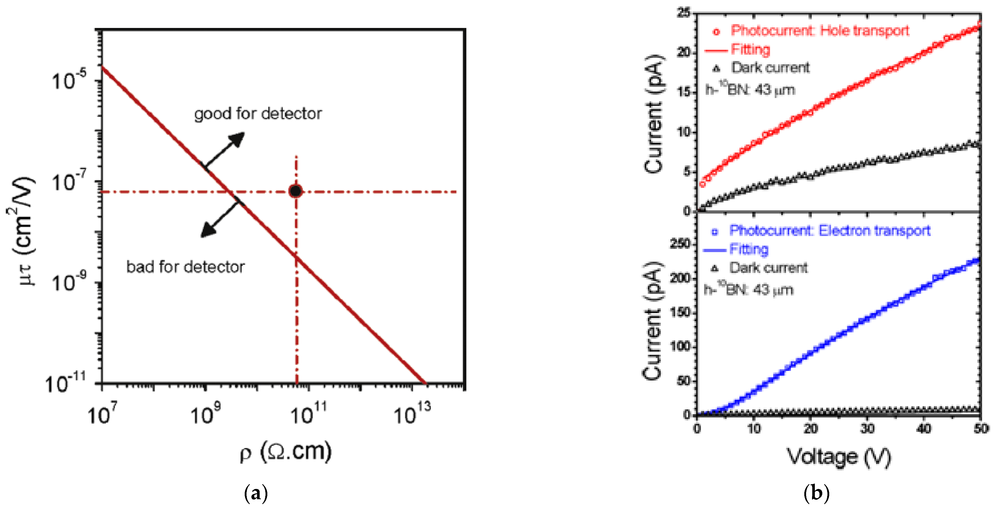
3.4. Mobility Lifetime Product
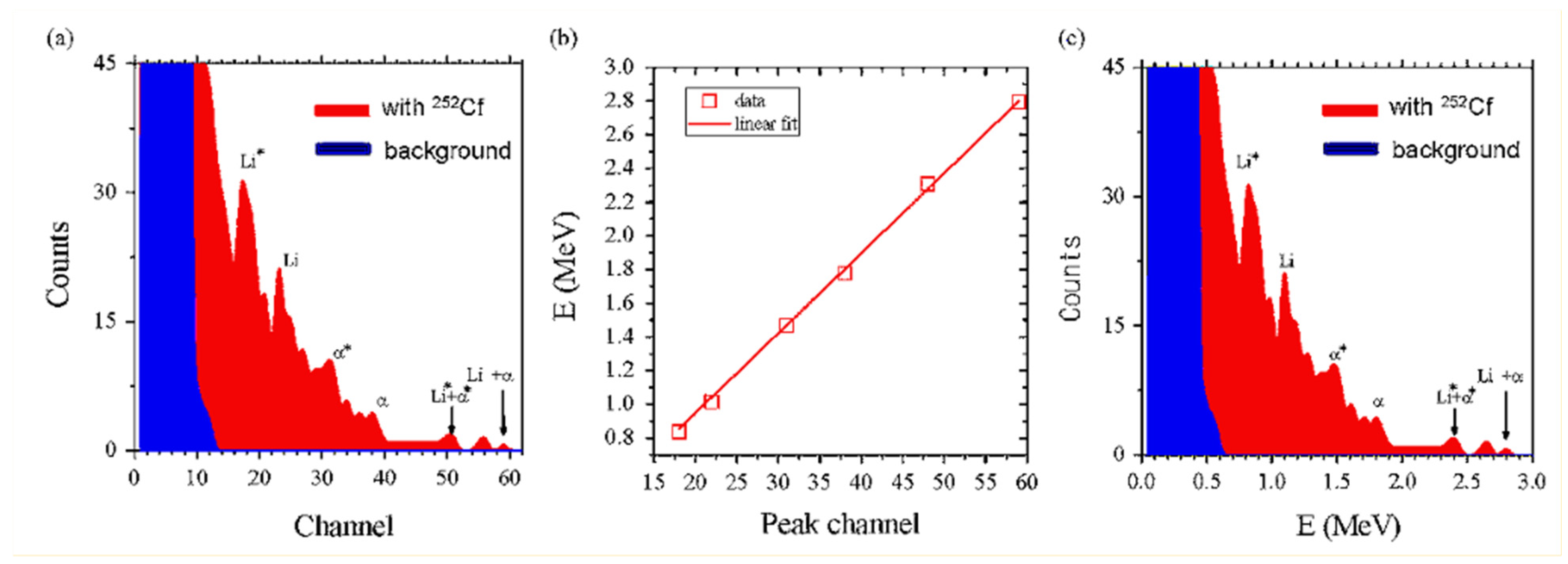
3.5. Pulse Height Spectra and Energy Resolution
3.6. Device Efficiency
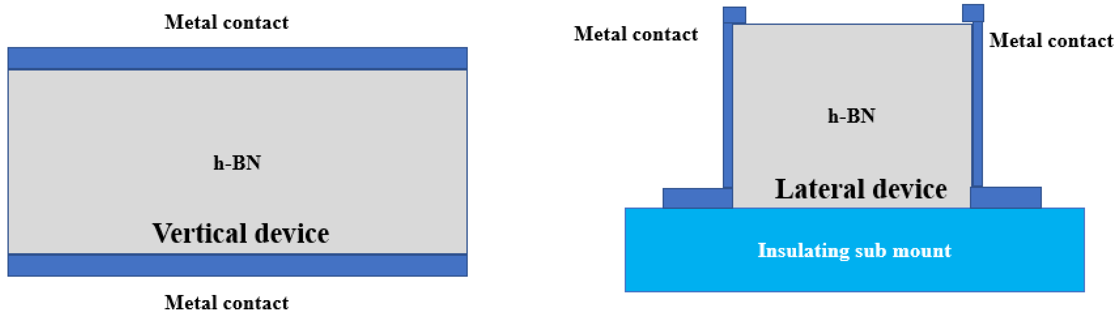
3.7. Lateral vs. Vertical Devices
4. Conclusions
Supplementary Materials
Author Contributions
Funding
Data Availability Statement
Acknowledgments
Conflicts of Interest
References
- U.S. Department of Energy (DOE). DOE Fundamentals Handbook Nuclear Physics Volume 2 of 2.; U.S. Department of Energy: Washington, DC, USA, 1993; Volume 1, p. 36. [Google Scholar]
- McGregor, D.S.; Klann, R.T.; Gersch, H.K.; Yang, Y.H. Thin-film-coated bulk GaAs detectors for thermal and fast neutron measurements. Nucl. Instrum. Methods Phys. Res. Sect. A Accel. Spectrom. Detect. Assoc. Equip. 2001, 466, 126–141. [Google Scholar] [CrossRef]
- Coleman, R. The Application of Neutron Activation Analysis to Forensic Science. J. Forensic Sci. Soc. 1967, 6, 19–22. [Google Scholar] [CrossRef]
- Youmans, A.H. Conduction Counter for Radioactivity Well Logging. U.S. Patent 2,760,078, 21 August 1956. [Google Scholar]
- Yazbeck, J. Investigations of Hexagonal Boron Nitride as a Semiconductor for Neutron Detection. Ph.D. Thesis, Kansas State University, Manhattan, NY, USA, August 2012. [Google Scholar]
- Caruso, A.N. The Physics of Solid-State Neutron Detector Materials and Geometries. J. Phys. Condens. Matter 2010, 22, 443201. [Google Scholar] [CrossRef] [PubMed]
- Beckurts, K.H.; Wirtz, K. Neutron Physics; Springer Science & Business Media: Berlin/Heidelberg, Germany, 29 June 2013. [Google Scholar]
- Knoll, G.F. Radiation Detection and Measurement, 3rd ed.; John Wiley and Sons Inc.: New York, NY, USA, 2009; pp. 1–796. [Google Scholar]
- Kouzes, R.T.; Ely, J.H.; Erikson, L.E.; Kernan, W.J.; Lintereur, A.T.; Siciliano, E.R.; Stephens, D.L.; Stromswold, D.C.; Van Ginhoven, R.M.; Woodring, M.L. Neutron Detection Alternatives to 3He for National Security Applications. Nucl. Instrum. Methods Phys. Res. Sect. A Accel. Spectrom. Detect. Assoc. Equip. 2010, 623, 1035–1045. [Google Scholar] [CrossRef]
- Angelone, M. Neutron Detection: Principles, Methods, Issues (and Tips) Maurizio Angelone; ENEA Frascati: Rome, Italy, 2009. [Google Scholar]
- McGregor, D.S.; Shultis, J.K. Spectral identification of thin-film-coated and solid-form semiconductor neutron detectors. Nucl. Instrum. Methods Phys. Res. Sect. A Accel. Spectrom. Detect. Assoc. Equip. 2004, 517, 180–188. [Google Scholar] [CrossRef]
- Nikolic, R.J.; Cheung, C.L.; Reinhardt, C.E.; Wang, T.F. Roadmap for High Efficiency Solid-State Neutron Detectors. In Proceedings of the Optoelectronic Devices: Physics, Fabrication, and Application II, Boston, MA, USA, 23–26 October 2005; Volume 15, p. 601305. [Google Scholar] [CrossRef] [Green Version]
- Nikolic, R.J.; Conway, A.M.; Reinhardt, C.E.; Graff, R.T.; Wang, T.F.; Deo, N.; Cheung, C.L. Pillar structured thermal neutron detector with 6:1 aspect ratio. Appl. Phys. Lett. 2008, 93, 133502. [Google Scholar] [CrossRef] [Green Version]
- Bellinger, S.L.; Fronk, R.G.; McNeil, W.J.; Sobering, T.J.; McGregor, D.S. Enhanced variant designs and characteristics of the microstructured solid-state neutron detector. Nucl. Instrum. Methods Phys. Res. Sect. A Accel. Spectrom. Detect. Assoc. Equip. 2011, 652, 387–391. [Google Scholar] [CrossRef]
- Clinton, J. Optimization and Characterization of a Novel Self Powered Solid State Neutron Detector. Ph.D. Thesis, Rensselaer Polytechnic Institute, Troy, NY, USA, December 2011. [Google Scholar]
- Shao, Q.; Voss, L.F.; Conway, A.M.; Nikolic, R.J.; Dar, M.A.; Cheung, C.L. High Aspect Ratio Composite Structures with 48.5% Thermal Neutron Detection Efficiency. Appl. Phys. Lett. 2013, 102, 063505. [Google Scholar] [CrossRef]
- Osberg, K.; Schemm, N.; Balkir, S.; Brand, J.I.; Hallbeck, M.S.; Dowben, P.A.; Hoffman, M.W. A handheld neutron-detection sensor system utilizing a new class of boron carbide diode. IEEE Sens. J. 2006, 6, 1531–1538. [Google Scholar] [CrossRef] [Green Version]
- Doan, T.C.; Majety, S.; Grenadier, S.; Li, J.; Lin, J.Y.; Jiang, H.X. Fabrication and Characterization of Solid-State Thermal Neutron Detectors Based on Hexagonal Boron Nitride Epilayers. Nucl. Instrum. Methods Phys. Res. Sect. A Accel. Spectrom. Detect. Assoc. Equip. 2014, 748, 84–90. [Google Scholar] [CrossRef]
- Jiang, H.X.; Lin, J.Y. Hexagonal boron nitride epilayers: Growth, optical properties and device applications. ECS J. Solid State Sci. Technol. 2016, 6, Q3012. [Google Scholar] [CrossRef]
- Huang, K.C.; Dahal, R.; Lu, J.J.Q.; Weltz, A.; Danon, Y.; Bhat, I.B. Scalable Large-Area Solid-State Neutron Detector with Continuous p-n Junction and Extremely Low Leakage Current. Nucl. Instrum. Methods Phys. Res. Sect. A Accel. Spectrom. Detect. Assoc. Equip. 2014, 763, 260–265. [Google Scholar] [CrossRef]
- Shultis, J.K.; McGregor, D.S. Design and performance considerations for perforated semiconductor thermal-neutron detectors. Nucl. Instrum. Methods Phys. Res. Sect. A Accel. Spectrom. Detect. Assoc. Equip. 2009, 606, 608–636. [Google Scholar] [CrossRef]
- Alam, M.D.; Nasim, S.S.; Hasan, S. Recent progress in CdZnTe based room temperature detectors for nuclear radiation monitoring. Prog. Nucl. Energy 2021, 140, 103918. [Google Scholar] [CrossRef]
- McGregor, D.S.; Hammig, M.D.; Yang, Y.H.; Gersch, H.K.; Klann, R.T. Design considerations for thin film coated semiconductor thermal neutron detectors—I: Basics regarding alpha particle emitting neutron reactive films. Nucl. Instrum. Methods Phys. Res. Sect. A Accel. Spectrom. Detect. Assoc. Equip. 2003, 500, 272–308. [Google Scholar] [CrossRef]
- Gersch, H.K.; McGregor, D.S.; Simpson, P.A. The effect of incremental gamma-ray doses and incremental neutron fluences upon the performance of self-biased 10B-coated high-purity epitaxial GaAs thermal neutron detectors. Nucl. Instrum. Methods Phys. Res. Sect. A Accel. Spectrom. Detect. Assoc. Equip. 2002, 489, 85–98. [Google Scholar] [CrossRef]
- Dahal, R.; Huang, K.C.; Clinton, J.; Licausi, N.; Lu, J.Q.; Danon, Y.; Bhat, I. Self-Powered Micro-Structured Solid State Neutron Detector with Very Low Leakage Current and High Efficiency. Appl. Phys. Lett. 2012, 100, 243507. [Google Scholar] [CrossRef]
- Nelson, R.O.; Vogel, S.C.; Hunter, J.F.; Watkins, E.B.; Losko, A.S.; Tremsin, A.S.; Borges, N.P.; Cutler, T.E.; Dickman, L.T.; Espy, M.A.; et al. Neutron imaging at LANSCE—From cold to ultrafast. J. Imaging 2018, 4, 45. [Google Scholar] [CrossRef] [Green Version]
- Rose, A. Sputtered boron films on silicon surface barrier detectors. Nucl. Instrum. Methods 1967, 52, 166–170. [Google Scholar] [CrossRef]
- Doty, P.F. Boron Nitride Solid State Neutron Detector. U.S. Patent 6,727,504, 27 April 2004. [Google Scholar]
- Robinson, J. Novel Carborane Derived Semiconducting Thin Films for Neutron Detection and Device Applications. Doctoral Dissertation, University of North Texas, Denton, TX, USA, 2015. [Google Scholar]
- McGregor, D.S.; Unruh, T.C.; McNeil, W.J. Thermal neutron detection with pyrolytic boron nitride. Nucl. Instrum. Methods Phys. Res. Sect. A Accel. Spectrom. Detect. Assoc. Equip. 2008, 591, 530–533. [Google Scholar] [CrossRef]
- Li, J.; Dahal, R.; Majety, S.; Lin, J.Y.; Jiang, H.X. Hexagonal Boron Nitride Epitaxial Layers as Neutron Detector Materials. Nucl. Instrum. Methods Phys. Res. Sect. A Accel. Spectrom. Detect. Assoc. Equip. 2011, 654, 417–420. [Google Scholar] [CrossRef]
- Jiang, H.; Lin, J.; Li, J.; Maity, A.; Grenadier, S. Solid-State Neutron Detector. U.S. Patent 20200135958A1, 14 July 2018. [Google Scholar]
- Nava, F.; Bertuccio, G.; Cavallini, A.; Vittone, E. Silicon Carbide and Its Use as a Radiation. Meas. Sci. Technol. 2008, 19, 102001. [Google Scholar] [CrossRef]
- Del Sordo, S.; Abbene, L.; Caroli, E.; Mancini, A.M.; Zappettini, A.; Ubertini, P. Progress in the Development of CdTe and CdZnTe Semiconductor Radiation Detectors for Astrophysical and Medical Applications. Sensors 2009, 9, 3491–3526. [Google Scholar] [CrossRef] [PubMed]
- Laturia, A.; Van de Put, M.L.; Vandenberghe, W.G. Dielectric Properties of Hexagonal Boron Nitride and Transition Metal Dichalcogenides: From Monolayer to Bulk. NPJ 2D Mater. Appl. 2018, 2, 6. [Google Scholar] [CrossRef] [Green Version]
- Klein, C.A. Bandgap dependence and related features of radiation ionization energies in semiconductors. J. Appl. Phys. 1968, 39, 2029–2038. [Google Scholar] [CrossRef]
- Li, J.; Majety, S.; Dahal, R.; Zhao, W.P.; Lin, J.Y.; Jiang, H.X. Dielectric Strength, Optical Absorption, and Deep Ultraviolet Detectors of Hexagonal Boron Nitride Epilayers. Appl. Phys. Lett. 2012, 101, 171112. [Google Scholar] [CrossRef] [Green Version]
- Majety, S.; Li, J.; Cao, X.K.; Dahal, R.; Lin, J.Y.; Jiang, H.X. Metal-Semiconductor-Metal Neutron Detectors Based on Hexagonal Boron Nitride Epitaxial Layers. In Proceedings of the Hard X-Ray, Gamma-Ray, and Neutron Detector Physics XIV, San Diego, CA, USA, 2–16 August 2012. [Google Scholar]
- Grenadier, S.; Li, J.; Lin, J.; Jiang, H. Dry Etching Techniques for Active Devices Based on Hexagonal Boron Nitride Epilayers. J. Vac. Sci. Technol. A Vac. Surf. Film. 2013, 31, 61517. [Google Scholar] [CrossRef] [Green Version]
- Majety, S.; Cao, X.K.; Dahal, R.; Pantha, B.N.; Li, J.; Lin, J.Y.; Jiang, H.X. Semiconducting Hexagonal Boron Nitride for Deep Ultraviolet Photonics. In Proceedings of the Quantum Sensing and Nanophotonic Devices IX, San Diego, CA, USA, 21–26 January 2012. [Google Scholar] [CrossRef]
- Li, J.; Gui, G.; Zhong, J. Tunable Bandgap Structures of Two-Dimensional Boron Nitride. J. Appl. Phys. 2008, 104, 094311. [Google Scholar] [CrossRef]
- Pacilé, D.; Meyer, J.C.; Girit, Ç.Ö.; Zettl, A. The two-dimensional phase of boron nitride: Few-atomic-layer sheets and suspended membranes. Appl. Phys. Lett. 2008, 92, 133107. [Google Scholar] [CrossRef]
- Li, L.; Chen, Y.I.; Zhang, H.; Li, L.H.; Chen, Y.; Behan, G.; Petravic, M.; Glushenkov, A.M. Large-Scale Mechanical Peeling of Boron Nitride Nanosheets by Low-Energy Ball Milling Large-Scale Mechanical Peeling of Boron Nitride Nanosheets by Low-Energy Ball Milling. Artic. J. Mater. Chem. 2011, 21, 11862–11866. [Google Scholar] [CrossRef]
- Coleman, J.N.; Lotya, M.; O’Neill, A.; Bergin, S.D.; King, P.J.; Khan, U.; Nicolosi, V. Two-dimensional nanosheets produced by liquid exfoliation of layered materials. Science 2011, 331, 568–571. [Google Scholar] [CrossRef] [Green Version]
- Lin, Y.; Williams, T.V.; Connell, J.W. Soluble, exfoliated hexagonal boron nitride nanosheets. J. Phys. Chem. Lett. 2010, 1, 277–283. [Google Scholar] [CrossRef]
- Han, W.Q.; Wu, L.; Zhu, Y.; Watanabe, K.; Taniguchi, T. Structure of Chemically Derived Mono-and Few-Atomic-Layer Boron Nitride Sheets. Appl. Phys. Lett. 2008, 93, 223103. [Google Scholar] [CrossRef]
- Zhi, C.; Ueda, S.; Zeng, H.; Wang, X.; Tian, W.; Wang, X.; Bando, Y.; Golberg, D. Weak Morphology Dependent Valence Band Structure of Boron Nitride. J. Appl. Phys. 2013, 114, 054306. [Google Scholar] [CrossRef]
- Jin, C.; Lin, F.; Suenaga, K.; Iijima, S. Fabrication of a Freestanding Boron Nitride Single Layer and Its Defect Assignments. APS Phys. 2009, 102, 195505. [Google Scholar] [CrossRef] [Green Version]
- Warner, J.H.; Rümmeli, M.H.; Bachmatiuk, A.; Büchner, B. Atomic Resolution Imaging and Topography of Boron Nitride Sheets Produced by Chemical Exfoliation. ACS Nano 2010, 4, 1299–1304. [Google Scholar] [CrossRef]
- Meyer, J.C.; Chuvilin, A.; Algara-Siller, G.; Biskupek, J.; Kaiser, U. Selective Sputtering and Atomic Resolution Imaging of Atomically Thin Boron Nitride Membranes. Nano Lett. 2009, 9, 2683–2689. [Google Scholar] [CrossRef]
- Li, X.; Hao, X.; Zhao, M.; Wu, Y.; Yang, J.; Tian, Y.; Qian, G. Exfoliation of Hexagonal Boron Nitride by Molten Hydroxides. Adv. Mater. 2013, 25, 2200–2204. [Google Scholar] [CrossRef]
- Wang, X.; Zhi, C.; Li, L.; Zeng, H.; Li, C.; Mitome, M.; Golberg, D.; Bando, Y. “Chemical Blowing” of Thin-Walled Bubbles: High-Throughput Fabrication of Large-Area, Few-Layered BN and C x-BN Nanosheets. Adv. Mater. 2011, 23, 4072–4076. [Google Scholar] [CrossRef]
- Wang, X.-B.; Weng, Q.; Wang, X.; Li, X.; Zhang, J.; Liu, F.; Jiang, X.F.; Guo, H.; Xu, N.; Golberg, D.; et al. Biomass-Directed Synthesis of 20 g High-Quality Boron Nitride Nanosheets for Thermoconductive Polymeric Composites. ACS Nano 2014, 8, 9081–9088. [Google Scholar] [CrossRef]
- Nag, A.; Raidongia, K.; Hembram, K.P.S.S.; Datta, R.; Waghmare, U.V.; Rao, C.N.R. Graphene Analogues of BN: Novel Synthesis and Properties. ACS Nano 2010, 4, 1539–1544. [Google Scholar] [CrossRef]
- Zhang, X.; Qin, J.; Xue, Y.; Yu, P.; Zhang, B.; Wang, L.; Liu, R. Effect of aspect ratio and surface defects on the photocatalytic activity of ZnO nanorods. Sci. Rep. 2014, 4, 4596. [Google Scholar] [CrossRef] [PubMed] [Green Version]
- Gao, R.; Yin, L.; Wang, C.; Qi, Y.; Lun, N.; Zhang, L.; Liu, Y.X.; Kang, L.; Wang, X. High-Yield Synthesis of Boron Nitride Nanosheets with Strong Ultraviolet. J. Phys. Chem. C 2009, 113, 15160–15165. [Google Scholar] [CrossRef]
- Hasan, S.; Mamun, A.; Hussain, K.; Gaevski, M.; Ahmad, I.; Khan, A. Growth Evolution of High-Quality MOCVD Aluminum Nitride Using Nitrogen as Carrier Gas on the Sapphire Substrate. J. Mater. Res. 2021, 36, 4360–4369. [Google Scholar] [CrossRef]
- Hasan, S.; Mamun, A.; Hussain, K.; Patel, D.; Gaevski, M.; Ahmad, I.; Khan, A. Investigation of MOCVD Grown Crack-Free 4 Μm Thick Aluminum Nitride Using Nitrogen as a Carrier Gas. MRS Adv. 2021, 6, 456–460. [Google Scholar] [CrossRef]
- Boo, J.H.; Rohr, C.; Ho, W. MOCVD of BN and GaN Thin Films on Silicon: New Attempt of GaN Growth with BN Buffer Layer. J. Cryst. Growth 1998, 189, 439–444. [Google Scholar] [CrossRef]
- Coudurier, N.; Boichot, R.; Mercier, F.; Reboud, R.; Lay, S.; Blanquet, E.; Pons, M. Growth of boron nitride on (0001) AlN templates by High Temperature-Hydride Vapor Phase Epitaxy (HT-HVPE). Phys. Procedia 2013, 46, 102–106. [Google Scholar] [CrossRef]
- Snure, M.; Paduano, Q.; Kiefer, A. Effect of Surface Nitridation on the Epitaxial Growth of Few-Layer Sp2BN. J. Cryst. Growth 2016, 436, 16–22. [Google Scholar] [CrossRef] [Green Version]
- Wu, Q.; Yan, J.; Zhang, L.; Chen, X.; Wei, T.; Li, Y.; Liu, Z.; Wei, X.; Zhang, Y.; Wang, J.; et al. Growth Mechanism of AlN on Hexagonal BN/Sapphire Substrate by Metal-Organic Chemical Vapor Deposition. CrystEngComm 2017, 19, 5849–5856. [Google Scholar] [CrossRef]
- Hasan, S.; Jewel, M.U.; Karakalos, S.G.; Gaevski, M.; Ahmad, I. Comparative Spectroscopic Study of Aluminum Nitride Grown by MOCVD in H2 and N2 Reaction Environment. Coatings 2022, 12, 924. [Google Scholar] [CrossRef]
- Tay, R.Y. Chemical Vapor Deposition Growth and Characterization of Two-Dimensional Hexagonal Boron Nitride; Springer: Singapore, Singapore, 2018; ISBN 978-981-10-8808-7. [Google Scholar]
- Nakamura, K.; Sasaki, T. Boron Nitride Films Prepared by MOCVD. J. Solid State Chem. 2000, 154, 101–106. [Google Scholar] [CrossRef]
- Han, M.; Ryu, B.D.; Ko, K.B.; Jo, C.H.; Lim, C.-H.; Cuong, T.V.; Han, N.; Hong, C.H. Characteristics of Aluminum Nitride Films on Hexagonal Boron Nitride Buffer Layers Using Various Growth Methods through Metal Organic Chemical Vapor Deposition. J. Cryst. Growth 2019, 507, 316–320. [Google Scholar] [CrossRef]
- Yang, F.H. Modern Metal-Organic Chemical Vapor Deposition (MOCVD) Reactors and Growing Nitride-Based Materials; Woodhead Publishing Limited: Cambridge, UK, 2013; ISBN 9780857095077. [Google Scholar]
- Patriarche, G.; Ougazzaden, A.; Li, X.; Alam, S.; Sundaram, S.; Halfaya, Y. Wafer-Scale MOVPE Growth and Characterization of Highly Ordered h-BN on Patterned Sapphire Substrates. J. Cryst. Growth 2018, 509, 40–43. [Google Scholar] [CrossRef]
- Lee, H.-J.; Honda, Y.; Amano, H.; Bae, S.-Y.; Yang, X.; Pristovsek, M.; Nagamatsu, K.; Liu, Y.; Nitta, S. Growth of Hexagonal Boron Nitride on Sapphire Substrate by Pulsed-Mode Metalorganic Vapor Phase Epitaxy. J. Cryst. Growth 2017, 482, 1–8. [Google Scholar] [CrossRef]
- Eichler, J.; Lesniak, C. Boron nitride (BN) and BN composites for high-temperature applications. J. Eur. Ceram. Soc. 2008, 28, 1105–1109. [Google Scholar] [CrossRef]
- Tingsuwatit, A.; Maity, A.; Grenadier, S.J.; Li, J.; Lin, J.Y.; Jiang, H.X. Boron nitride neutron detector with the ability for detecting both thermal and fast neutrons. Appl. Phys. Lett. 2022, 120, 232103. [Google Scholar] [CrossRef]
- Caban, P.A.; Teklinska, D.; Michalowski, P.P.; Gaca, J.; Wojcik, M.; Grzonka, J.; Ciepielewski, P.; Mozdzonek, M.; Baranowski, J.M. The Role of Hydrogen in Carbon Incorporation and Surface Roughness of MOCVD-Grown Thin Boron Nitride. J. Cryst. Growth 2018, 498, 71–76. [Google Scholar] [CrossRef]
- Halfaya, Y.; Sundaram, S.; Patriarche, G.; Li, X.; Alam, S.; Salvestrini, J.P.; Voss, P.L.; Ougazzaden, A.; Ayari, T. MOVPE van Der Waals Epitaxial Growth of AlGaN/AlGaN Multiple Quantum Well Structures with Deep UV Emission on Large Scale 2D h-BN Buffered Sapphire Substrates. J. Cryst. Growth 2018, 507, 352–356. [Google Scholar] [CrossRef]
- Kobayashi, Y.; Akasaka, T. Hexagonal BN Epitaxial Growth on (0001) Sapphire Substrate by MOVPE. J. Cryst. Growth 2008, 310, 5044–5047. [Google Scholar] [CrossRef]
- Jana, M.; Singh, R.N. Progress in CVD Synthesis of Layered Hexagonal Boron Nitride with Tunable Properties and Their Applications. Int. Mater. Rev. 2018, 63, 162–203. [Google Scholar] [CrossRef]
- Maity, A.; Grenadier, S.J.; Li, J.; Lin, J.Y.; Jiang, H.X. Hexagonal Boron Nitride Neutron Detectors with High Detection Efficiencies. J. Appl. Phys. 2018, 123, 044501. [Google Scholar] [CrossRef]
- Zheng, F.; Xiao, X.; Xie, J.; Zhou, L.; Li, Y.; Dong, H. Structures, properties and applications of two-dimensional metal nitrides: From nitride MXene to other metal nitrides. 2D Mater. 2022, 9, 022001. [Google Scholar] [CrossRef]
- Yang, X.; Nitta, S.; Pristovsek, M.; Liu, Y.; Nagamatsu, K.; Kushimoto, M.; Amano, H. Interface amorphization in hexagonal boron nitride films on sapphire substrate grown by metalorganic vapor phase epitaxy. Appl. Phys. Express 2018, 11, 051002. [Google Scholar] [CrossRef]
- Maity, A.; Doan, T.C.; Li, J.; Lin, J.Y.; Jiang, H.X. Realization of Highly Efficient Hexagonal Boron Nitride Neutron Detectors. Appl. Phys. Lett. 2016, 109, 072101. [Google Scholar] [CrossRef]
- Maity, A.; Grenadier, S.J.; Li, J.; Lin, J.Y.; Jiang, H.X. Toward Achieving Flexible and High Sensitivity Hexagonal Boron Nitride Neutron Detectors. Appl. Phys. Lett. 2017, 111, 033507. [Google Scholar] [CrossRef] [Green Version]
- Ahmed, K.; Dahal, R.; Weltz, A.; Lu, J.J.Q.; Danon, Y.; Bhat, I.B. Solid-State Neutron Detectors Based on Thickness Scalable Hexagonal Boron Nitride. Appl. Phys. Lett. 2017, 110, 023503. [Google Scholar] [CrossRef] [Green Version]
- Doan, T.C.; Marty, A.; Li, J.; Lin, J.Y.; Jiang, H.X. Thermal Neutron Detectors Based on Hexagonal Boron Nitride Epilayers. In Proceedings of the Hard X-Ray, Gamma-Ray, and Neutron Detector Physics XVIII, San Diego, CA, USA, 28 August–1 September 2016; Volume 9968, p. 99680S. [Google Scholar] [CrossRef]
- Doan, T.C.; Majety, S.; Grenadier, S.; Li, J.; Lin, J.Y.; Jiang, H.X. Hexagonal Boron Nitride Thin Film Thermal Neutron Detectors with High Energy Resolution of the Reaction Products. Nucl. Instrum. Methods Phys. Res. Sect. A Accel. Spectrom. Detect. Assoc. Equip. 2015, 783, 121–127. [Google Scholar] [CrossRef]
- Maity, A.; Grenadier, S.J.; Li, J.; Lin, J.Y.; Jiang, H.X. High Sensitivity Hexagonal Boron Nitride Lateral Neutron Detectors. Appl. Phys. Lett. 2019, 114, 222102. [Google Scholar] [CrossRef]
- Maity, A.; Grenadier, S.J.; Li, J.; Lin, J.Y.; Jiang, H.X. High Efficiency Hexagonal Boron Nitride Neutron Detectors with 1 Cm2 Detection Areas. Appl. Phys. Lett. 2020, 116, 142102. [Google Scholar] [CrossRef] [Green Version]
- Dong, C.; Huang, Q.; Ma, X.; Yao, J.; Xiong, H.; Shen, F.; Chen, J.; Zhang, J.; Zhou, R. Readout electronics for thermal neutron detector array. Nucl. Instrum. Methods Phys. Res. Sect. A Accel. Spectrometers Detect. Assoc. Equip. 2019, 946, 162639. [Google Scholar] [CrossRef]
- Duclaux, L.; Nysten, B.; Issi, J.P.; Moore, A.W. Structure and low-temperature thermal conductivity of pyrolytic boron nitride. Phys. Rev. B 1992, 46, 3362. [Google Scholar] [CrossRef]
- Du, X.Z.; Li, J.; Lin, J.Y.; Jiang, H.X. The Origin of Deep-Level Impurity Transitions in Hexagonal Boron Nitride. Appl. Phys. Lett. 2015, 106, 021110. [Google Scholar] [CrossRef] [Green Version]
- Doan, T.C.; Li, J.; Lin, J.Y.; Jiang, H.X. Bandgap and Exciton Binding Energies of Hexagonal Boron Nitride Probed by Photocurrent Excitation Spectroscopy. Appl. Phys. Lett. 2016, 109, 122101. [Google Scholar] [CrossRef]
- Spieler, H.G.; Haller, E. Assessment of Present and Future Large-Scale Semiconductor Detector Systems. IEEE Trans. Nucl. Sci. 1985, 32, 419–426. [Google Scholar] [CrossRef] [Green Version]
- Many, A. High-Field Effects in Photoconducting Cadmium Sulphide. J. Phys. Chem. Solids 1965, 26, 575–578. [Google Scholar] [CrossRef]
- Maity, A.; Grenadier, S.J.; Li, J.; Lin, J.Y.; Jiang, H.X. Effects of Surface Recombination on the Charge Collection in H-BN Neutron Detectors. J. Appl. Phys. 2019, 125, 104501. [Google Scholar] [CrossRef]
- Cao, X.K.; Clubine, B.; Edgar, J.H.; Lin, J.Y.; Jiang, H.X. Two-Dimensional Excitons in Three-Dimensional Hexagonal Boron Nitride. Appl. Phys. Lett. 2013, 103, 191106. [Google Scholar] [CrossRef]
- Doan, T.C.; Li, J.; Lin, J.Y.; Jiang, H.X. Response of Alpha Particles in Hexagonal Boron Nitride Neutron Detectors. Appl. Phys. Lett. 2017, 110, 213502. [Google Scholar] [CrossRef] [Green Version]
- Dahal, R.; Ahmed, K.; Woei Wu, J.; Weltz, A.; Jian-Qiang Lu, J.; Danon, Y.; Bhat, I.B. Anisotropic Charge Carrier Transport in Free-Standing Hexagonal Boron Nitride Thin Films. Appl. Phys. Express 2016, 9, 065801. [Google Scholar] [CrossRef]


| Isotope | Cross Section in Barn (1 barn = 10−24 cm2) |
|---|---|
| 3He | 5333 |
| 6Li | 941 |
| 10B | 3838 |
| 113Cd | 20,600 |
| 235U | 681 |
| 135Xe | 2,720,000 |
| 199Hg | 2150 |
| Material | Si | Ge | CdTe | Cd0.5Zn0.5Te | 4H SiC | a-Se | h-BN |
|---|---|---|---|---|---|---|---|
| Crystal structure | Cubic | Cubic | Cubic | Cubic | Hexagonal | Amorphous | Hexagonal |
| Production method | CZ | CZ | THM | BM, THM | PVT-Bulk, CVD-epitaxy | HVTE-Thin film | MOCVD |
| Atomic number | 14 | 32 | 48,52 | 48,30,52 | 14,6 | 34 | 5,7 |
| Density | 2.33 | 5.33 | 6.2 | 5.78 | 3.21 | 6.4 | 2.18 |
| Bandgap | 1.12 | 0.67 | 1.5 | 1.6 | 3.27 | 2.24 | ~6.4 |
| Dielectric constant | 11.7 | 16.2 | 10.2 | ~11 | 9.7 | ~6 | 4.9 |
| e-h pair creation energy | 3.62 | 2.96 | 4.43 | 4.6 | 7.28 | ~50 | 18 |
| Resistivity | 104 | 50 | 109 | >1010 | >1012 | ~1013 | ~1013 |
| 3He | Scintillator Detector | B Coated Detector | BN Semiconductor Detector | |
|---|---|---|---|---|
| Particle generated by neutron | ions | photons | Ions, electrons, holes | Ions, electrons, holes |
| Active thickness | ≈10 cm | ≈1 mm | ≈100 μm | ≈100 μm |
| Key issue | Shortage of 3He gas | sensitivity | sensitivity | Suitable materials |
| Response speed | ≈1 ms | ≈1 ns | ≈1 ns | 1 ns |
| Intrinsic detection efficiency | high | Low | Low | High |
| Cost | High | Low | Low | Low |
| Portability | Poor | Medium | High | high |
| Precursors | Substrate | Carrier Gas | Growth Temp. (°C) | Pressure (Torr) | Film Quality | Ref. |
|---|---|---|---|---|---|---|
| Triethylamine borane and ammonia (V/III ratio varied between 450 and 2700) | C-plane sapphire (varying surface nitridation) | H2 | 900 (nitridation temperature) 1100 (growth temperature | 20 torr | Good epitaxy achieved | [61] |
| Pulse mode injection of precursors triethylamine borane and ammonia | C-plane sapphire substrate | H2 | 1350 | 10 torr | Different pulse time was tried, and optimum parameter was achieved | [77] |
| Triethyl borane and ammonia (V/III ratio varied between 2000 and 4000) | Sapphire substrate | Carrier gas flow rate was varied (H2) | Buffer layer at ≈600–800 Main epilayer ≥ 1400 | Not mentioned | 380 arcsec FWHM with excellent stoichiometric ratio and surface morphology | [77,78,79,80,81,82] |
| Same precursor was used with a varied NH3 injection rate | Sapphire substrate | H2; 27 slm | 1000 | 3.85 kPa | Effect of NH3 injection rate was observed and optimized | [78] |
| No. | Material Thickness | Contact Type | Device Type | Area of the Device | Ref. |
|---|---|---|---|---|---|
| 1 | 0.3 μm | Ti/Al | Lateral | 4.8 mm2 | [18] |
| 2 | 0.3 μm | Ti/Al | Lateral | 12 mm2 | [83] |
| 3 | 0.3–43 | Ti/Al | vertical | Not mentioned | [82] |
| 4 | 43 μm | Ni/Au | vertical | 1 mm2 | [79] |
| 5 | 2.5–15 μm | Ti/Ti | vertical | 40 mm2 −14 mm2 | [81] |
| 6 | 50 μm | Ni/Au | Vertical | 9 mm2 | [80] |
| 7 | 50 μm | Ni/Au and Ti/Al | vertical | 1 mm2 | [76] |
| 8 | 90 μm | Ni/Au | Lateral | 29 mm2 | [84] |
| 9 | 100 μm | Ni/Au | Lateral | 1 cm2 | [85] |
| No. | Material Thickness in μm | for Electrons | for Holes | Resistivity | Material Specimen in mCi (Millicurie) | Area of the Device in mm2 | Bias Voltage in V | Time Measured | Efficiency | Reference |
|---|---|---|---|---|---|---|---|---|---|---|
| 1 | 0.3 | 4.5 × 10⁻⁸ | 7.1 × 10⁻⁹ | 5.3 × 10¹⁰ | 2.4 | 4.8 | 240 | 26 h | Not mentioned | [18] |
| 2 | 50 | 1.0 × 10⁻⁶ | 1.0 × 10⁻⁶ | Not mentioned | Not mentioned | 1 | 200 | Not mentioned | 58% | [76] |
| 3 | 43 | 8.3 × 10⁻⁷ | 2.2 × 10⁻⁵ | 1.0 × 10¹³ | 0.93 | 1 | 400 | 10 min | 51.40% | [79] |
| 4 | 50 | 2.0 × 10⁻⁶ | 1.0 × 10⁻⁵ | 1.0 × 10¹³ | 0.77 | 9 | 200 | 15 min | 53% | [80] |
| 5 | 2.5–15 | 3.0 × 10⁻⁷ | 5.0 × 10⁻⁸ | 3.0 × 10⁹ | Not mentioned | 14–40 | 700, 450, 600, 700 | Not mentioned | 4.21–21.37% | [81] |
| 6 | 0.3–43 | 3.3 × 10⁻⁷ | 3.3 × 10⁻⁷ | 5.0 × 10¹⁰ | Not mentioned | Not mentioned | Variable | 20 min | 51.40% (43 μm) | [82] |
| 7 | 0.3 | 2.83 × 10⁻⁷ | 2.83 × 10⁻⁷ | 5.0 × 10¹⁰ | 1.6 | 12 | 20 | Not mentioned | Not mentioned | [83] |
| 8 | 90 | 1.0 × 10⁻⁴ | 1.0 × 10⁻⁴ | Not mentioned | 0.5 | 29 | 400 | 15 min | 50% | [84] |
| 9 | 100 | 5.0 × 10⁻³ | 5.0 × 10⁻³ | 1.0 × 10¹² | 0.45 | 100 | 500 | 15 min | 59% | [85] |
Publisher’s Note: MDPI stays neutral with regard to jurisdictional claims in published maps and institutional affiliations. |
© 2022 by the authors. Licensee MDPI, Basel, Switzerland. This article is an open access article distributed under the terms and conditions of the Creative Commons Attribution (CC BY) license (https://creativecommons.org/licenses/by/4.0/).
Share and Cite
Hasan, S.; Ahmad, I. Progress in Hexagonal Boron Nitride (h-BN)-Based Solid-State Neutron Detector. Electron. Mater. 2022, 3, 235-251. https://doi.org/10.3390/electronicmat3030020
Hasan S, Ahmad I. Progress in Hexagonal Boron Nitride (h-BN)-Based Solid-State Neutron Detector. Electronic Materials. 2022; 3(3):235-251. https://doi.org/10.3390/electronicmat3030020
Chicago/Turabian StyleHasan, Samiul, and Iftikhar Ahmad. 2022. "Progress in Hexagonal Boron Nitride (h-BN)-Based Solid-State Neutron Detector" Electronic Materials 3, no. 3: 235-251. https://doi.org/10.3390/electronicmat3030020
APA StyleHasan, S., & Ahmad, I. (2022). Progress in Hexagonal Boron Nitride (h-BN)-Based Solid-State Neutron Detector. Electronic Materials, 3(3), 235-251. https://doi.org/10.3390/electronicmat3030020