Review

Majority and Minority Charge Carrier Traps in n-Type 4H-SiC Studied by Junction Spectroscopy Techniques

Ruđer Bošković Institute, Bijenička 54, 10000 Zagreb, Croatia
*
Author to whom correspondence should be addressed.
Electron. Mater. 2022, 3(1), 115-123; https://doi.org/10.3390/electronicmat3010011
Submission received: 28 January 2022 / Revised: 11 February 2022 / Accepted: 9 March 2022 / Published: 14 March 2022
(This article belongs to the Special Issue Feature Papers of Electronic Materials II)

Abstract

:
In this review, we provide an overview of the most common majority and minority charge carrier traps in n-type 4H-SiC materials. We focus on the results obtained by different applications of junction spectroscopy techniques. The basic principles behind the most common junction spectroscopy techniques are given. These techniques, namely, deep-level transient spectroscopy (DLTS), Laplace DLTS (L-DLTS), and minority carrier transient spectroscopy (MCTS), have led to recent progress in identifying and better understanding the charge carrier traps in n-type 4H-SiC materials.

1. Introduction

Today, 4H-SiC materials are regarded as one of the most promising types of materials for electronic devices. It has the largest bandgap among all SiC polytypes, and due to the high and isotropic mobility of charge carriers, it is preferred as a material for power electronics [1], bipolar devices [2], and quantum sensing [3]. Moreover, it has found applications in radiation detection too [1,4,5].
Even wider applicability of 4H-SiC has mostly been hindered by electrically active deep level defects present in the material. Electrically active defects introduce energy levels into the bandgap that act as traps for charge carriers. The majority charge carrier traps in n-type 4H–SiC material have been systematically investigated for many years. On the other hand, minority charge carrier traps in n-type 4H–SiC material have been much less investigated [6,7,8,9].
Junction spectroscopy technique is a term describing measurements performed on a semiconductor junction using electrical or electro-optical techniques [10]. The role of the junction is to create a depletion region, as its usage brings an important advantage over other bulk techniques. The advantage is that it is much easier to manipulate the occupancy of defects producing energy levels in the bandgap within the depletion region than in bulk region [10]. The most common junction spectroscopy technique is deep-level transient spectroscopy (DLTS). DLTS can detect defects in concentrations around 1010 cm−3 [10]. It provides information regarding the activation energy for electron and hole emission, capture cross-section, and concentration of defects. However, the main problem associated with DLTS is the lack of energy resolution (i.e., it is almost impossible to resolve two closely spaced deep energy levels). An improvement came in another junction spectroscopy technique called Laplace DLTS (L-DLTS), which brought an order of magnitude better energy resolution (meV) [11].
While DLTS is mostly used for studying the electrically active defects associated with majority charge carrier traps, minority charge carrier traps have been much less investigated. The basic principles of minority transient spectroscopy techniques were described by Hamilton et al. [12], and later by Brunwin et al. [13].
In this review, we provide an overview of the main majority and minority charge carrier traps in n-type 4H-SiC materials. We focus this overview on the recent advances achieved by means of junction spectroscopy techniques. Moreover, the basic principles behind the junction spectroscopy techniques responsible for these advances are provided. The main aim of this mini-review is to provide a basic description of junction spectroscopy techniques supported by examples from different studies on n-type 4H-SiC materials for graduate students and early-stage researchers.

2. Materials and Methods

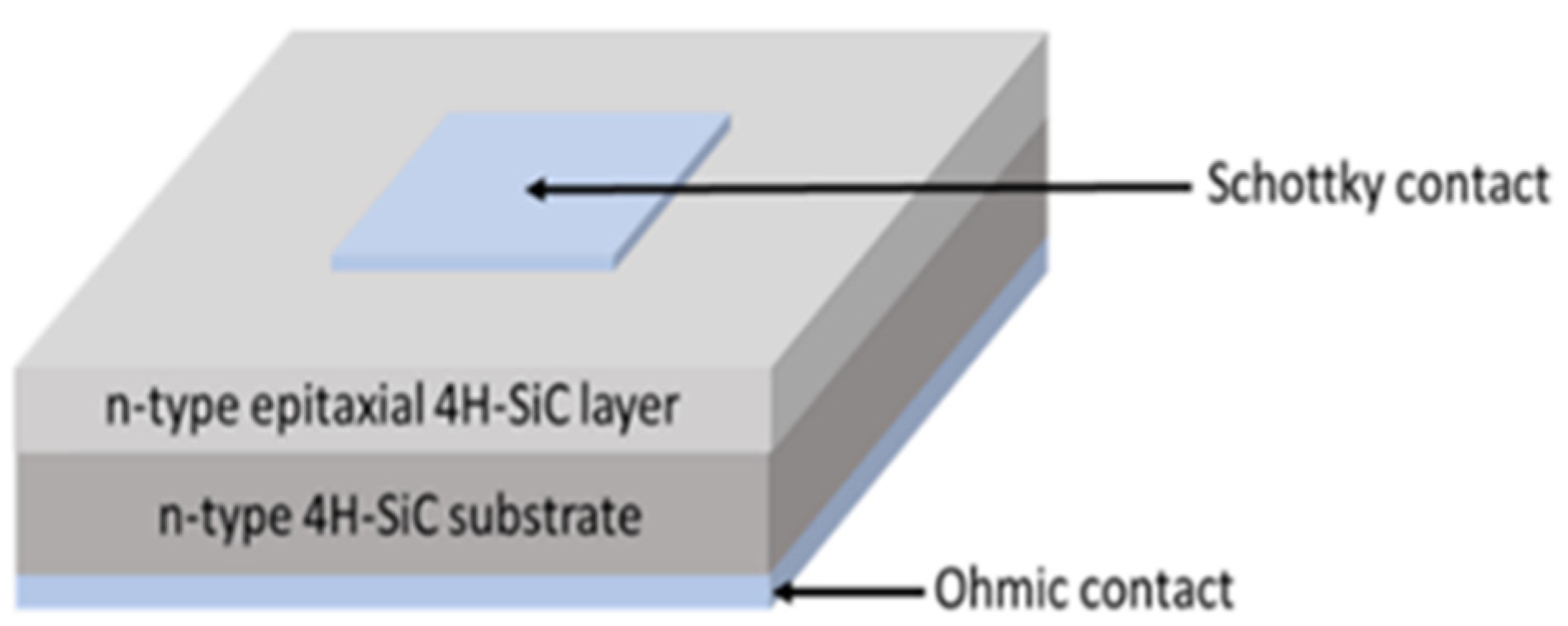
2.1. Schottky Barrier Diode

As mentioned above, we need a junction to apply junction spectroscopy techniques for studying the electrically active defects in semiconductors. One of the basic junctions is the Schottky barrier diode (SBD). Figure 1 shows a schematic cross-section of a typical n-type 4H-SiC SBD.
SBD is formed when a metal and an n-type semiconductor are joined. Due to band alignment, a depletion space charge region (a volume depleted of charge carriers) is created at the semiconductor side of the junction [5]. As we apply the external bias, we enable the transport of electrons, and a net current will flow through the SBD. The SBD is reversely biased when a negative voltage (VR) is applied to the metal with respect to the semiconductor. The SBD is kept under reverse bias when junction transient spectroscopies are applied.
Typical n-type 4H-SiC SBDs are produced on nitrogen-doped 4H-SiC epitaxial layers. The epitaxial layers are grown on thick silicon carbide substrate. The Schottky barriers are formed by thermal evaporation of nickel through a metal mask with openings, while ohmic contacts are formed on the backside of the silicon carbide substrate by nickel sintering.

2.2. Measurement Techniques

Electrically active defects introduce energy levels into the bandgap of a semiconductor, which act as traps for charge carriers. We can distinguish between majority and minority charge carrier traps. Majority carrier traps in semiconductors have been successfully and extensively studied by DLTS for decades [10,11], while minority charge carrier traps have been much less studied. In principle, it is possible to investigate these traps using DLTS by applying forward bias [14], but more reliable results can be obtained by using minority carrier transient spectroscopy (MCTS). The main principles of DLTS and MCTS will be described next. More detailed information about these techniques is given elsewhere [10,11].

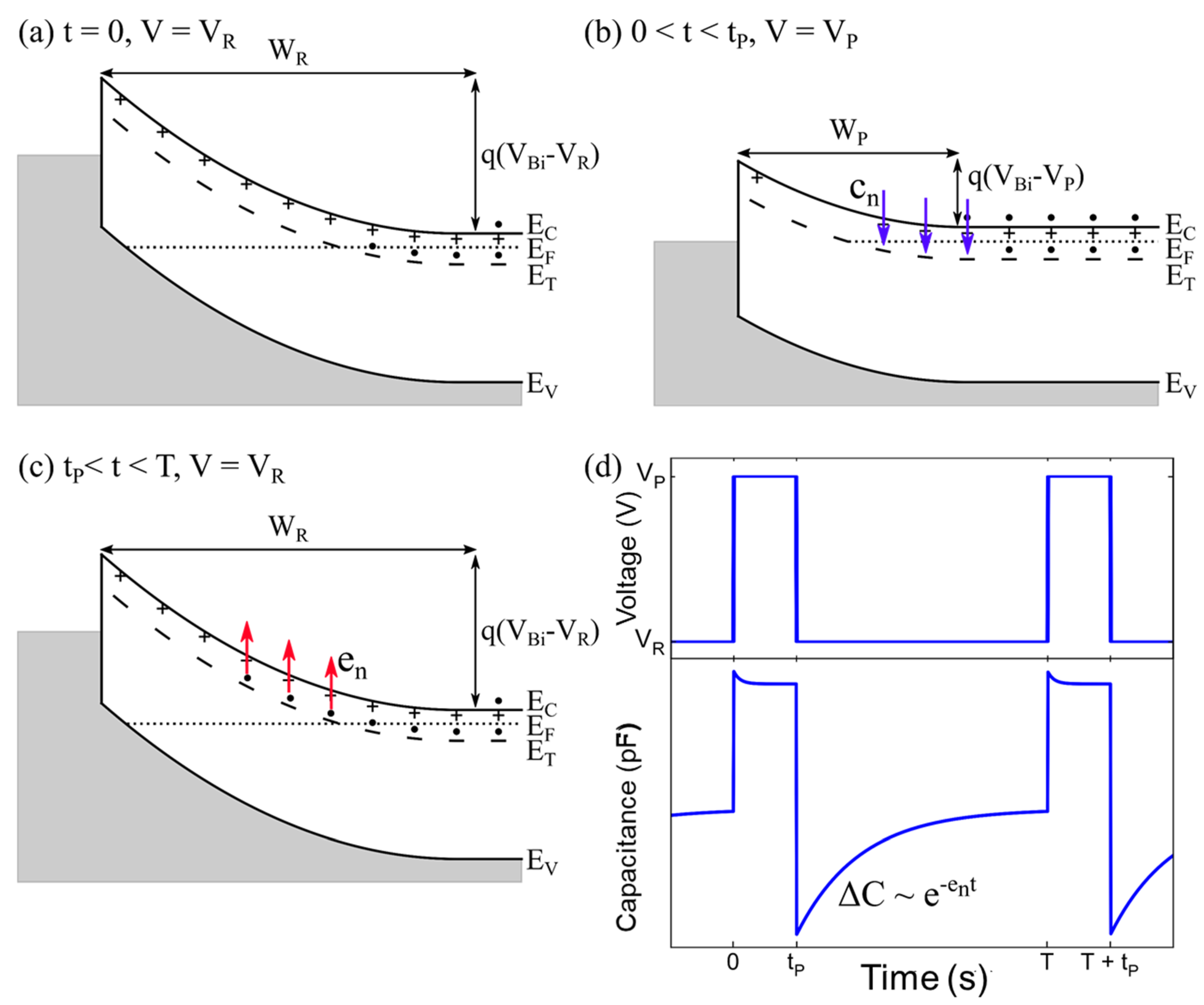
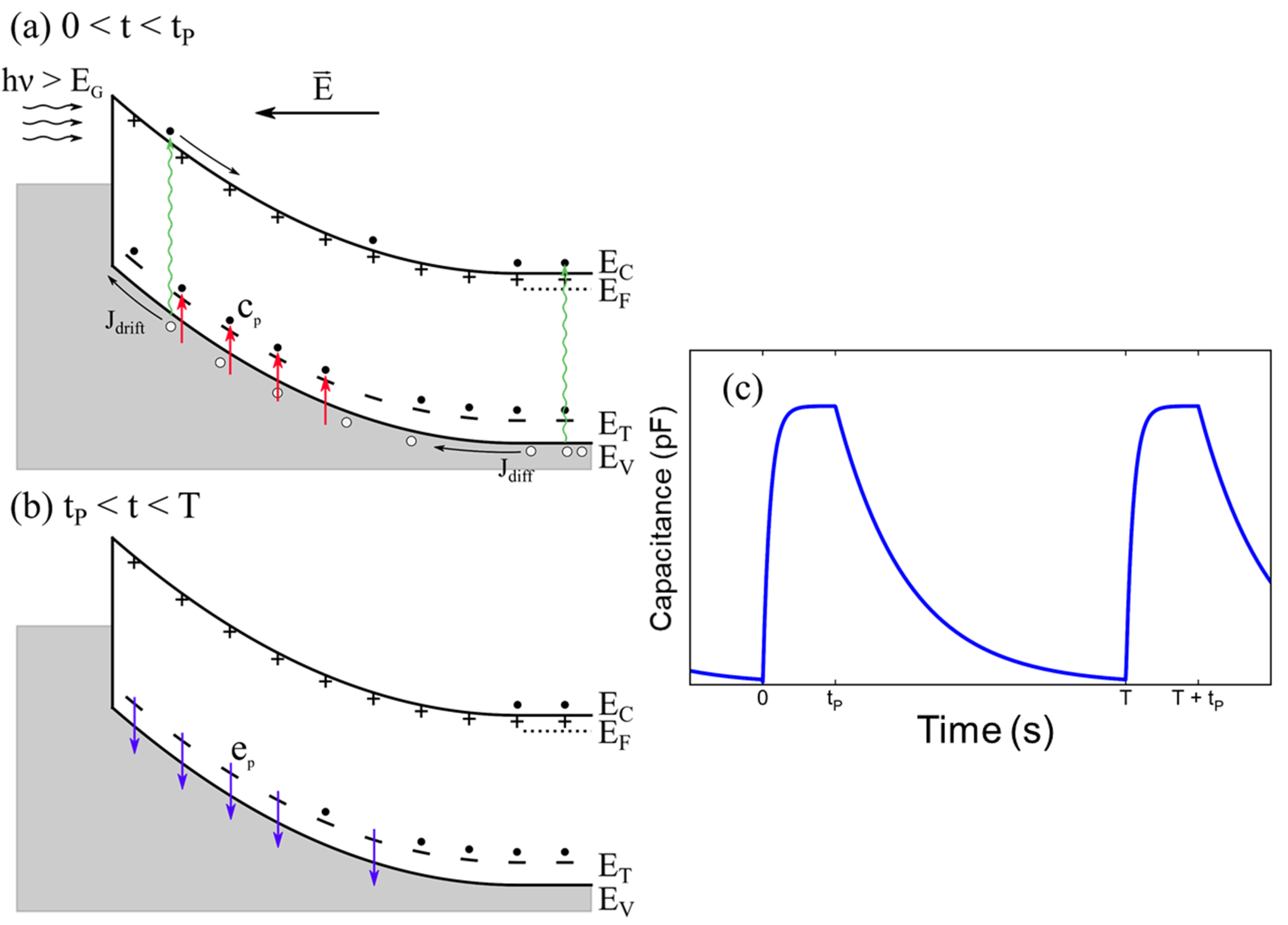
2.2.1. Deep-Level Transient Spectroscopy (DLTS)

Basic DLTS measurement consists of the repetitive filling and emptying of deep levels (ET) in the depletion region of the SBD by a bias pulse, as shown in Figure 2. The n-type SBD is operated under reverse bias VR (Figure 2a), which is reduced to VP during a bias pulse (Figure 2b). Empty traps, residing in the former depletion region, will be able to capture free carriers and become occupied (Figure 2b). After restoring the original bias VR, the charge in the depletion region will be lower than before, due to the trapped charge carriers (Figure 2c). These carriers will be released again through thermal emission, which proceeds exponentially in time. This thermal discharging of the occupied traps is monitored by measuring the capacitance of the reverse biased diode as a function of time after the filling pulse (Figure 2d).
The transient analysis and the problems with the signal–noise ratio not only for DLTS, but for MCTS and L-DLTS as well, will not be addressed here, as that goes beyond this mini-review paper. This information can be found elsewhere [10,11,12,13].

2.2.2. Minority Carrier Transient Spectroscopy (MCTS)

The basic principle of MCTS measurement is slightly different, as minority charge carriers are optically generated by use of above-bandgap light [10]. The MCTS measurement consists of the repetitive filling and emptying of deep levels (ET) by optical pulses with an energy (hν) just above the bandgap energy (Eg), as shown in Figure 3. The minority charge carriers are captured during the optical pulse (Figure 3a), followed by the emission after the optical pulse (Figure 3b). Optical excitation can be applied through a semi-transparent Schottky contact, or from the back. If the sample thickness is greater than the minority carrier diffusion length, then the sample should be thinned [10].

3. Electrically Active Defects in n-Type 4H-SiC

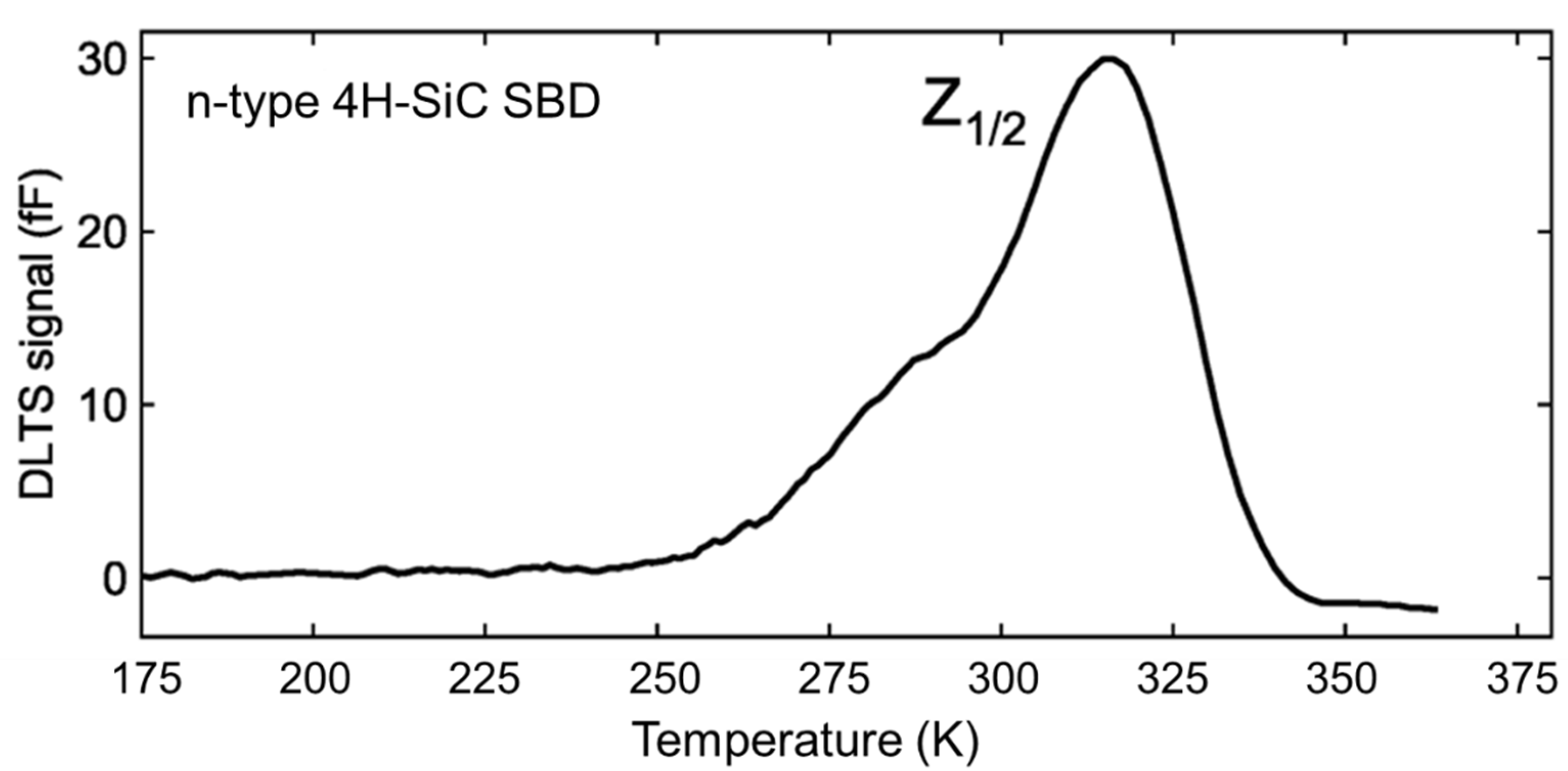
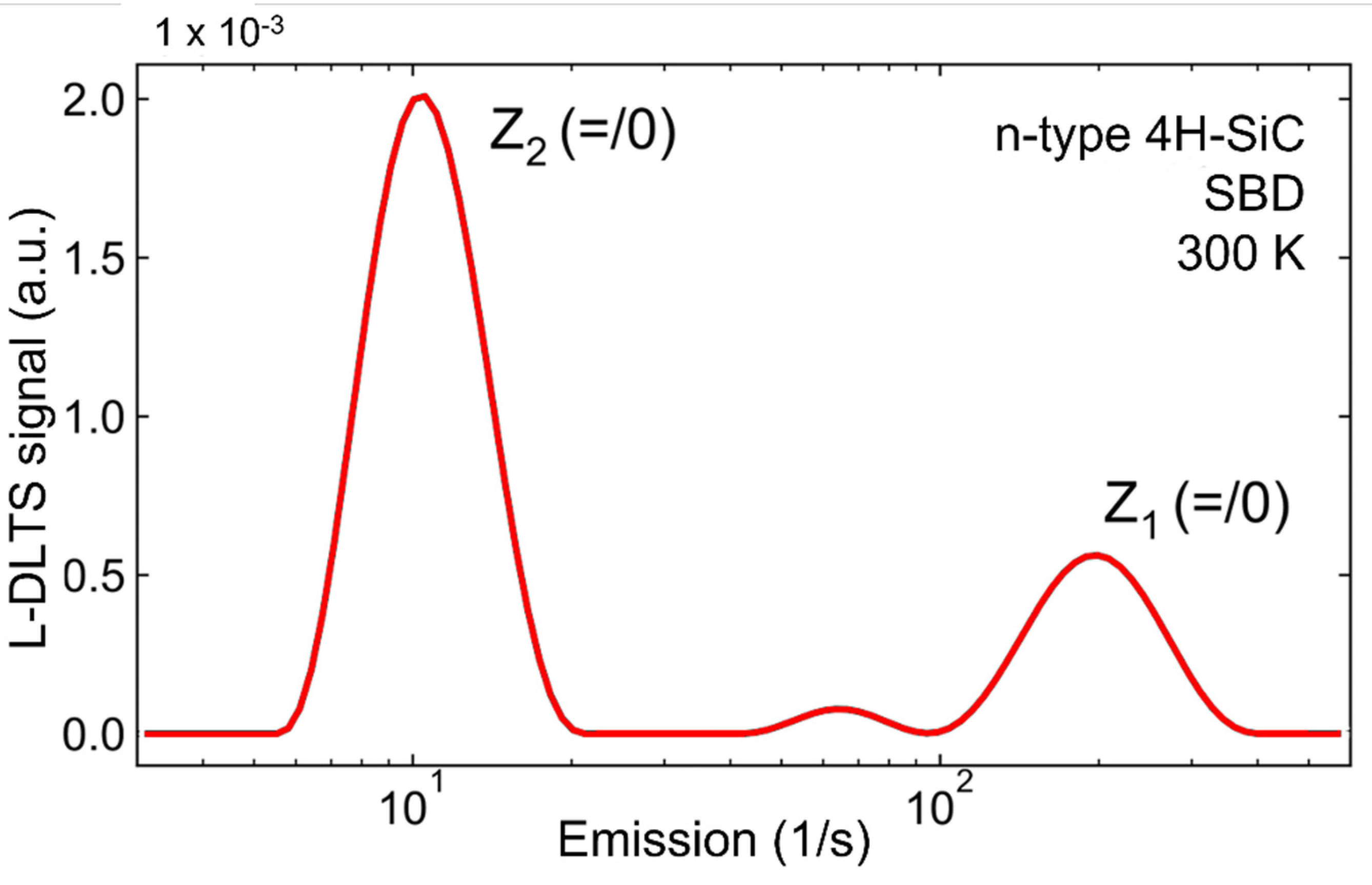
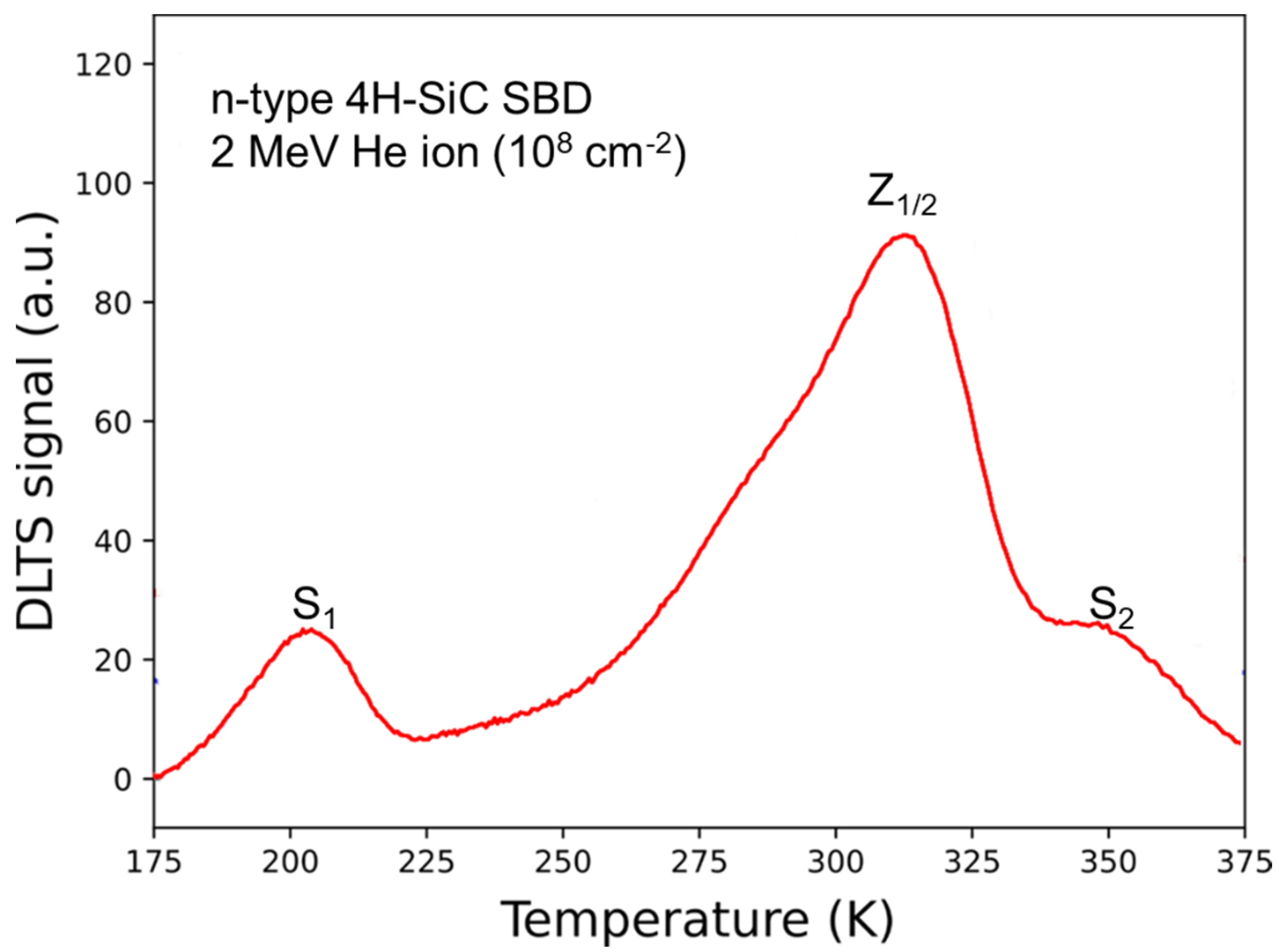
3.1. Majority Charge Carrier Traps

Figure 4 shows a typical DLTS spectrum for the as-grown n-type 4H-SiC SBD. One peak, labelled as Z1/2, is observed. The estimated activation energy for electron emission is EC − 0.67 eV. It should be noted that since 4H-SiC is a wide bandgap material, DLTS measurements are usually performed in the wider temperature range, 80–700 K.
Son et al. [17] were the first to ascribe Z1/2 to (=/0) transition from the carbon vacancy (VC). Carbon vacancy (Vc) is the most studied defect in n-type 4H-SiC. It is introduced during the crystal growth and upon irradiation [18].
As we can see in Figure 4, the DLTS peak is rather asymmetric. Hemmingsson et al. [19] showed that Z1/2 is the superposition of two almost identical Z1 and Z2 transitions, which cannot be resolved by DLTS. This problem (too closely spaced deep energy levels) is an ideal case for the application of another junction spectroscopy technique, L-DLTS. L-DLTS is an isothermal technique in which the capacitance transient (measurements follow the same principle as described in Figure 2) is averaged at a fixed temperature. It provides a spectral plot of a processed capacitance signal against emission rate rather than against temperature. Moreover, L-DLTS provides an energy resolution in meV. More details on L-DLTS can be found elsewhere [11].
Recently, using L-DLTS measurements, direct evidence that Z1/2 consists of two components has been observed, namely Z1 and Z2, with activation energies for electron emission of Ec − 0.59 and Ec − 0.67 eV, respectively. These were ascribed to (=/0) transitions of Vc located at hexagonal (-h) and pseudo-cubic (-k) sites of the 4H-SiC crystal, respectively [20,21]. Figure 5 shows an L-DLTS spectrum for the as-grown 4H-SiC SBD. Two emission lines (Z1 and Z2) arising from the Z1/2 DLTS peak are clearly resolved.
Figure 6 shows the DLTS spectrum for the 2 MeV He ion-implanted n-type 4H-SiC SBD. In addition to the Z1/2, 2 MeV He ion implantation has introduced two deep level defects, namely S1 and S2. Estimated activation energies for electron emissions for S1 and S2, are Ec − 0.40, and Ec − 0.70, respectively.
Using the L-DLTS measurements, Bathen et al. [3] have shown that S1 (in a proton-irradiated n-type 4H-SiC sample) has two emission lines arising from Vsi sitting at -k and -h lattice sites. This result was later confirmed by Capan et al. [22] when studying a neutron-irradiated n-type 4H-SiC SBD.
Deep level defect energies Ec−0.40 eV and Ec−0.70 eV have been reported in numerous studies for the proton-irradiated [3], ion-implanted [18,23], and neutron-irradiated [22,24] n-type 4H-SiC samples. All results indicated that these defects are intrinsic defects, either interstitials or vacancies. Recent progress in understanding the S1 and S2 defects has been achieved by Bathen et al. [3]. They have identified the S1 and S2 as VSi (−3/=) and VSi (=/−) charge states.
Moreover, two deep levels with identical activation energies for electron emission of Ec−0.40 and Ec−0.70 eV have been observed in the low-energy electron irradiated n-type 4H-SiC [25,26]. These defects (not shown here) are labeled as EH1 and EH3 and have been identified as carbon interstitial-related (Ci) defects [26].
In addition to the above-mentioned majority charge carrier traps (Z1/2, S1/2, EH1/3), we should not forget other majority carrier traps, which are usually present in the as-grown n-type 4H-SiC materials or are introduced by radiation or additional annealing. The most common traps are EH4/5 and EH6/7. The EH4/5 introduce peaks in the DLTS spectrum at around 450–500 K, while the EH6/7 introduce a broad DLTS peak at around 650 K (not shown here). They are assigned to carbon antisite-carbon vacancy (CAV) complex [27,28] and (0/++) transition of the Vc [17], respectively. The evidence that EH6/7 consists of two components was provided by Alfieri and Kimoto [29]. In their work, they resolved two energy levels at Ec − 1.30 and Ec − 1.49 eV, for EH6 and EH7, respectively, using L-DLTS measurements.

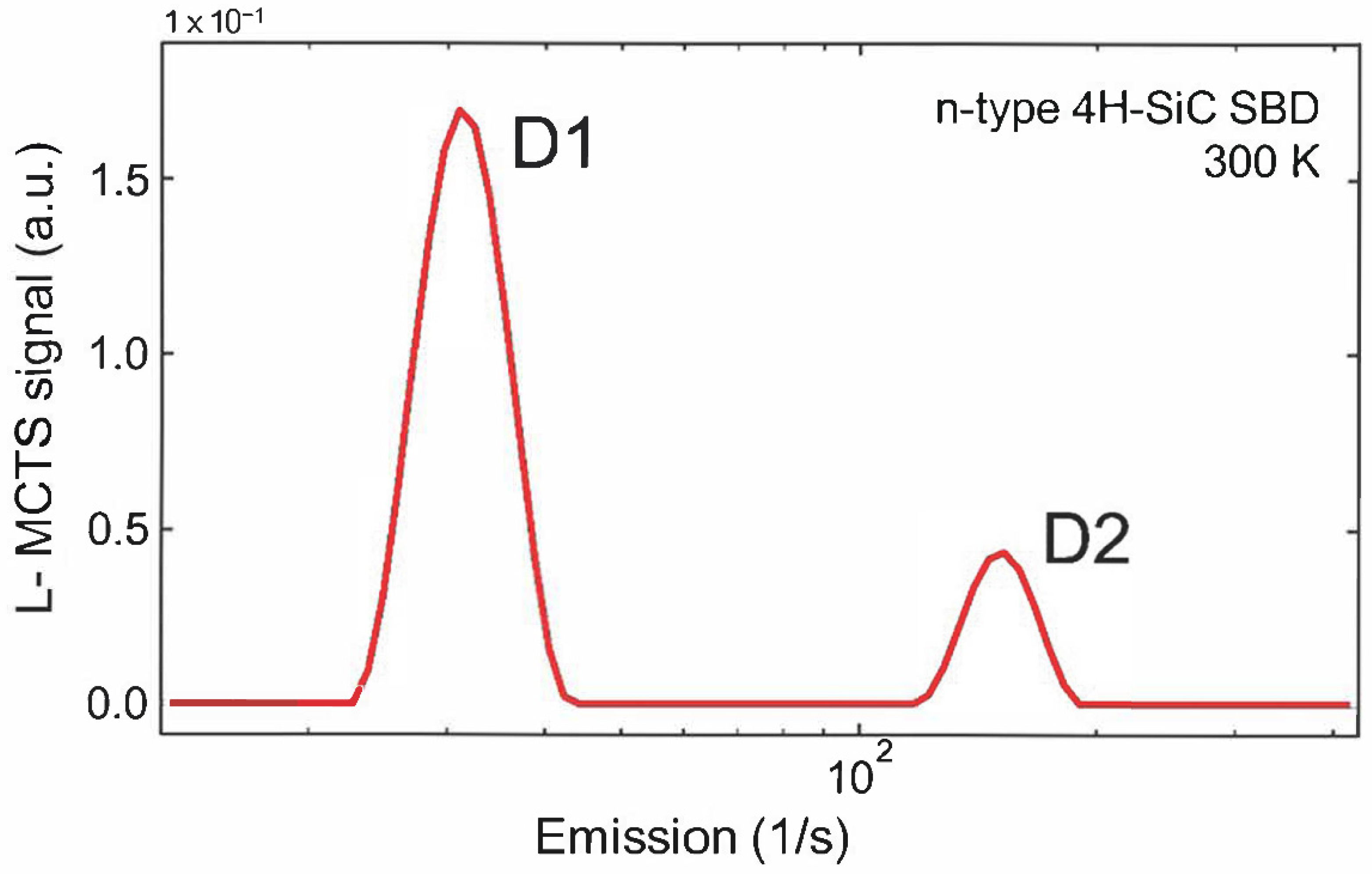
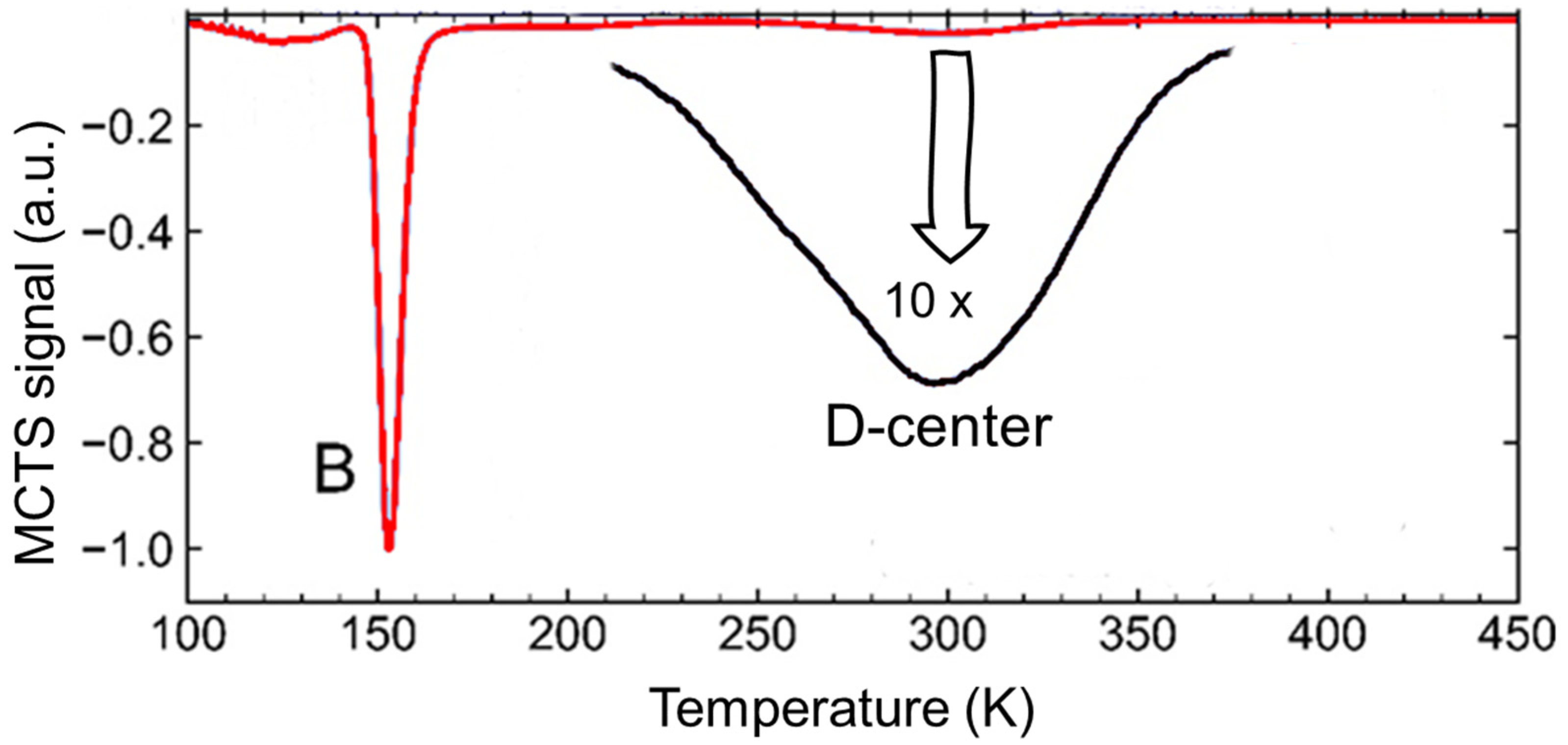
3.2. Minority Charge Carrier Traps

In the following text, we will focus on the minority charge carrier traps in an n-type 4H–SiC. Most published works are aluminum or boron related. In this paper, we will provide examples which are boron related. Boron is introduced in SiC intentionally for p-type doping, or unintentionally during crystal growth [2,7].
Figure 7 shows a MCTS spectrum for the n-type 4H-SiC SBD. Two MCTS peaks labeled as B and D-center (multiplied 10×, for clarity) with activation energies for hole emissions of Ev + 0.28 and Ev + 0.54 eV are detected.
Two boron-related defects, labelled as B (shallow boron) and D-center (deep boron state) have been extensively studied. They are assigned to substitutional boron atoms occupying the Si and C-site, respectively [30,31,32].
Similar to Z1/2, S1/2, and EH6/7, further improvements in studying the D-center by L-MCTS measurements have been made. Recent results have shown that the D-center has two emission lines, D1 and D2 (Figure 8), with activation energies for hole emissions of Ev + 0.49 eV and Ev + 0.57 eV, respectively. These emission lines are assigned to an isolated boron sitting at the C site, -h and -k site, respectively [31].
At the end of this section, we summarize the relevant information of the above-discussed majority and minority charge carrier traps. Figure 9 shows a graphical representation of the energy levels based on DLTS measurements. More information, including the energy levels observed by L-DLTS and MCTS measurements, is given in Table 1.

4. Conclusions

In this review paper, the basic principles behind the most used junction spectroscopy techniques, DLTS and MCTS, were given. We have provided examples from different studies on majority and minority charge carrier traps. Successful applications of junction spectroscopy techniques, which have led to better understanding of the charge carrier traps in n-type 4H-SiC materials, were highlighted.

Author Contributions

Funding acquisition, investigation, methodology, writing—original draft, and writing—review editing: I.C.; visualization, formal analysis, and investigation: T.B. All authors have read and agreed to the published version of the manuscript.

Funding

The present work was financially supported by the NATO Science for Peace and Security Programme, project No. G5674.

Data Availability Statement

Data is contained within the article.

Conflicts of Interest

The authors declare no conflict of interest.

References

  1. Kimoto, T.; Cooper, J.A. Fundamentals of Silicon Carbide Technology: Growth, Characterization, Devices, and Applications; John Wiley & Sons Singapore Pte. Ltd: Singapore, 2014. [Google Scholar] [CrossRef]
  2. Yang, A.; Murata, K.; Miyazawa, T.; Tawara, T.; Tsuchida, H. Analysis of carrier lifetimes in N+B-doped n-type 4H-SiC epilayers. J. Appl. Phys. 2019, 126, 055103. [Google Scholar] [CrossRef]
  3. Bathen, M.E.; Galeckas, A.; Müting, J.; Ayedh, H.M.; Grossner, U.; Coutinho, J.; Frodason, Y.K.; Vines, L. Electrical charge state identification and control for the silicon vacancy in 4H-SiC. NPJ Quantum Inf. 2019, 5, 111. [Google Scholar] [CrossRef] [Green Version]
  4. Radulović, V.; Yamazaki, Y.; Pastuović, Ž.; Sarbutt, A.; Ambrožič, K.; Bernat, R.; Ereš, Z.; Coutinho, J.; Ohshima, T.; Capan, I.; et al. Silicon carbide neutron detector testing at the JSI TRIGA reactor for enhanced border and port security. Nucl. Instrum. Methods Phys. Res. Sect. A Accel. Spectrometers Detect. Assoc. Equip. 2020, 972, 164122. [Google Scholar] [CrossRef]
  5. Coutinho, J.; Torres, V.J.B.; Capan, I.; Brodar, T.; Ereš, Z.; Bernat, R.; Radulović, V. Silicon carbide diodes for neutron detection. Nucl. Inst. Methods Phys. Res. A 2020, 986, 164793. [Google Scholar] [CrossRef]
  6. Zhang, J.; Storasta, L.; Bergman, J.P.; Son, N.T.; Janzén, E. Electrically active defects in n-type 4H-silicon carbide grown in a vertical hot-wall reactor. J. Appl. Phys. 2003, 93, 4708–4714. [Google Scholar] [CrossRef]
  7. Beyer, F.C.; Hemmingsson, C.G.; Leone, S.; Lin, Y.C.; Gällström, A.; Henry, A.; Janzén, E. Deep levels in iron doped n- and p-type 4H-SiC. J. Appl. Phys. 2011, 110, 123701. [Google Scholar] [CrossRef] [Green Version]
  8. Alfieri, G.; Kimoto, T. Detection of minority carrier traps in p-type 4H-SiC. Appl. Phys. Lett. 2014, 104, 092105. [Google Scholar] [CrossRef]
  9. Okuda, T.; Alfieri, G.; Kimoto, T.; Suda, J. Oxidation-induced majority and minority carrier traps in n-and p-type 4H-SiC. Appl. Phys. Express 2015, 8, 1301. [Google Scholar] [CrossRef]
  10. Peaker, A.R.; Markevich, V.P.; Coutinho, J. Tutorial: Junction spectroscopy techniques and deep-level defects in semiconductors. J. Appl. Phys. 2018, 123, 161559. [Google Scholar] [CrossRef] [Green Version]
  11. Peaker, A.R.; Dobachewski, L. Laplace-transform deep-level spectroscopy: The technique and its applications to the study of point defects in semiconductors. J. Appl. Phys. 2004, 96, 4689. [Google Scholar] [CrossRef] [Green Version]
  12. Hamilton, B.; Peaker, A.R.; Wight, D.R. Deep-state-controlled minority-carrier lifetime in n-type gallium phosphide. J. Appl. Phys. 1979, 50, 6373–6385. [Google Scholar] [CrossRef]
  13. Brunwin, R.; Hamilton, B.; Jordan, P.; Peaker, A.R. Detection of minority-carrier traps using transient spectroscopy. Electron. Lett. 1979, 15, 349–350. [Google Scholar] [CrossRef]
  14. Markevich, V.P.; Peaker, A.R.; Capan, I.; Lastovskii, S.B.; Dobaczewski, L.; Emtsev, V.V.; Abrosimov, N.V. Electrically active defects induced by irradiations with electrons, neutrons and ions in Ge-rich SiGe alloys. Phys. B Condens. Matter 2007, 401–402, 184–187. [Google Scholar] [CrossRef]
  15. Brodar, T. Characterization of Electrically Active Defects in 4H-SiC by Transient Spectroscopy Methods. Ph.D. Thesis, University of Zagreb, Zagreb, Serbia, 2021. [Google Scholar]
  16. Brodar, T.; Bakrač, L.; Capan, I.; Ohshima, T.; Snoj, L.; Radulović, V.; Pastuović, Ž. Depth Profile Analysis of Deep Level Defects in 4H-SiC Introduced by Radiation. Crystals 2020, 10, 845. [Google Scholar] [CrossRef]
  17. Son, N.T.; Trinh, X.T.; Løvlie, L.S.; Svensson, B.G.; Kawahara, K.; Suda, J.; Kimoto, T.; Umeda, T.; Isoya, J.; Makino, T.; et al. Negative-U System of Carbon Vacancy in 4H-SiC. Phys. Rev. Lett. 2012, 109, 187603. [Google Scholar] [CrossRef] [Green Version]
  18. Pastuović, Z.; Siegele, R.; Capan, I.; Brodar, I.; Sato, S.; Ohshima, T. Deep level defects in 4H-SiC introduced by ion implantation: The role of single ion regime. J. Phys. Condens. Matter 2017, 29, 475701. [Google Scholar] [CrossRef] [Green Version]
  19. Hemmingsson, C.G.; Son, N.T.; Ellison, A.; Zhang, J.; Janzén, E. Negative- U centers in 4 H silicon carbide. Phys. Rev. B 1998, 58, R10119–R10122. [Google Scholar] [CrossRef]
  20. Capan, I.; Brodar, T.; Pastuović, Z.; Siegele, R.; Ohshima, T.; Sato, S.I.; Makino, T.; Snoj, L.; Radulović, V.; Coutinho, J.; et al. Double negatively charged carbon vacancy at the h- and k-sites in 4H-SiC: Combined Laplace-DLTS and DFT study. J. Appl. Phys. 2018, 123, 161597. [Google Scholar] [CrossRef] [Green Version]
  21. Capan, I.; Brodar, T.; Coutinho, J.; Ohshima, T.; Markevich, V.P.; Peaker, A.R. Acceptor levels of the carbon vacancy in 4 H-SiC: Combining Laplace deep level transient spectroscopy with density functional modeling. J. Appl. Phys. 2018, 124, 245701. [Google Scholar] [CrossRef] [Green Version]
  22. Capan, I.; Brodar, T.; Makino, T.; Radulovic, V.; Snoj, L. M-Center in Neutron-Irradiated 4H-SiC. Crystals 2021, 11, 1404. [Google Scholar] [CrossRef]
  23. Capan, I.; Brodar, T.; Bernat, R.; Pastuović, Ž.; Makino, T.; Ohshima, T.; Gouveia, J.D.; Coutinho, J. M-center in 4H-SiC: Isothermal DLTS and first principles modeling studies. J. Appl. Phys. 2021, 130, 125703. [Google Scholar] [CrossRef]
  24. Brodar, T.; Capan, I.; Radulović, V.; Snoj, L.; Pastuović, Z.; Coutinho, J.; Ohshima, T. Laplace DLTS study of deep defects created in neutron-irradiated n-type 4H-SiC. Nucl. Instrum. Methods Phys. Res. Sect. B Beam Interact. Mater. Atoms. 2018, 437, 27–31. [Google Scholar] [CrossRef] [Green Version]
  25. Storasta, L.; Bergman, J.P.; Janzén, E.; Henry, A.; Lu, J. Deep levels created by low energy electron irradiation in 4H-SiC. J. Appl. Phys. 2004, 96, 4909–4915. [Google Scholar] [CrossRef]
  26. Alfieri, G.; Mihaila, A. Isothermal annealing study of the EH1 and EH3 levels in n-type 4H-SiC. J. Phys. Condens. Matter 2020, 32, 46. [Google Scholar] [CrossRef]
  27. Karsthof, R.; Bathen, M.E.; Galeckas, A.; Vines, L. Conversion pathways of primary defects by annealing in proton-irradiated n-type 4H-SiC. Phys. Rev. B 2020, 102, 184111. [Google Scholar] [CrossRef]
  28. Nakane, H.; Kato, M.; Ohkouchi, Y.; Trinh, X.T.; Ivanov, I.G.; Ohshima, T.; Son, N.T. Deep levels related to the carbon antisite–vacancy pair in 4H-SiC. J. Appl. Phys. 2021, 130, 065703. [Google Scholar] [CrossRef]
  29. Alfieri, G.; Kimoto, T. Resolving the EH6/7 level in 4H-SiC by Laplace-transform deep level transient spectroscopy. Appl. Phys. Lett. 2013, 102, 152108. [Google Scholar] [CrossRef] [Green Version]
  30. Capan, I.; Yamazaki, Y.; Oki, Y.; Brodar, T.; Makino, T.; Ohshima, T. Minority Carrier Trap in n-Type 4H–SiC Schottky Barrier Diodes. Crystals 2019, 9, 328. [Google Scholar] [CrossRef] [Green Version]
  31. Capan, I.; Brodar, T.; Yamazaki, Y.; Oki, Y.; Ohshima, T.; Chiba, Y.; Hijikata, Y.; Snoj, L.; Radulović, V. Influence of neutron radiation on majority and minority carrier traps in n-type 4H-SiC. Nucl. Inst. Methods Phys. Res. 2020, B478, 224–228. [Google Scholar] [CrossRef]
  32. Bockstedte, M.; Mattausch, A.; Pankratov, O. Boron in SiC: Structure and Kinetics. Mater Sci. Forum 2001, 353–356, 447–450. [Google Scholar] [CrossRef]
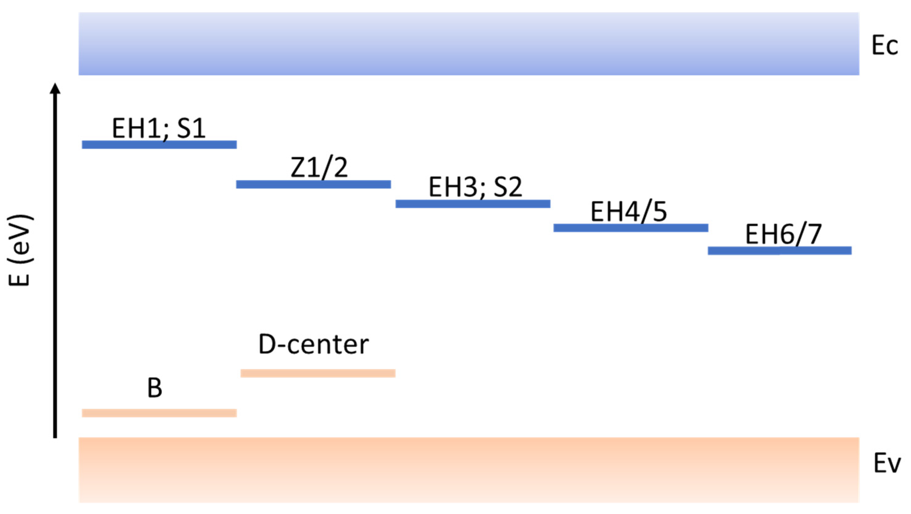
Figure 1. A schematic cross-section of a typical n-type 4H-SiC Schottky barrier diode (SBD).
Electronicmat 03 00011 g001
Figure 2. The basic principle of deep-level transient spectroscopy (DLTS) measurement: (a) equilibrium state with the applied reverse bias; (b) capture of the majority charge carriers in an n-type material while the pulse is applied VP; (c) emission of the trapped charge carriers; (d) the measured capacitance transient as a function of time. Here, tp is the filling pulse duration, WR and WP are the depletion region widths for the applied VR and Vp, respectively, en is the electron emission rate, and cn is the electron capture rate. Figure adapted from Ref. [15].
Electronicmat 03 00011 g002
Figure 3. The basic principle of minority carrier transient spectroscopy (MCTS) measurement: (a) capture of the minority charge carriers from the valence band to the deep level (ET) while optical pulses are applied; (b) emission of the minority charge carriers from the deep level after the optical pulse; (c) measured capacitance transient as a function of time. Figure adapted from Ref. [15]. Here, hν is the energy of the optical excitation, Jdrift and Jdiff are drift and diffusion current densities, respectively, tp is the optical pulse duration, ep is the hole emission rate, and cp is the hole capture rate.
Electronicmat 03 00011 g003
Figure 4. Typical DLTS spectrum for the as grown n-type 4H-SiC SBD. Data adapted from Ref. [16].
Electronicmat 03 00011 g004
Figure 5. Laplace DLTS (L-DLTS) spectrum for the as grown n-type 4H-SiC SBD measured at room temperature (RT) [15].
Electronicmat 03 00011 g005
Figure 6. DLTS spectrum for 2 MeV He ion-implanted n-type 4H-SiC SBD. Several deep level defects are observed: S1, Z1/2, and S2. Data adapted from Ref. [16].
Electronicmat 03 00011 g006
Figure 7. A normalized MCTS spectrum for the n-type 4H-SiC SBD. Data adapted from Ref. [32].
Electronicmat 03 00011 g007
Figure 8. L-MCTS spectrum for D-center in then-type 4H-SiC SBD measured at 300 K. Data adapted from Ref. [15].
Electronicmat 03 00011 g008
Figure 9. Graphical representation of the energy levels, based on DLTS measurements.
Electronicmat 03 00011 g009
Table 1. Details on the majority and minority charge carrier traps in n-type 4H-SiC materials.
Trap LabelIdentificationActivation Energy (eV)References
EH1CiEc − 0.40[25,26]
EH3CiEc − 0.70[25,26]
S1VSi (−3/−)Ec − 0.40[3,22]
S2VSi (=/−)Ec − 0.70[3,22]
Z1Vc (=/0)Ec − 0.59[17,19,20,21]
Z2Vc (=/0)Ec − 0.67[17,19,20,21]
EH4/5Csi-Vc (+/0)Ec − 1.10[27,28]
EH6Vc (0/++)Ec − 1.30[17,18,29]
EH7Vc (0/++)Ec − 1.40[17,18,29]
BBsiEv + 0.28[2,7,30,31,32]
D-centerBcEv + 0.54[2,7,30,31,32]
Publisher’s Note: MDPI stays neutral with regard to jurisdictional claims in published maps and institutional affiliations.

