
Structural Changes Induced by Heating in Sputtered NiO and Cr2O3 Thin Films as p-Type Transparent Conductive Electrodes


Abstract
1. Introduction
2. Materials and Methods
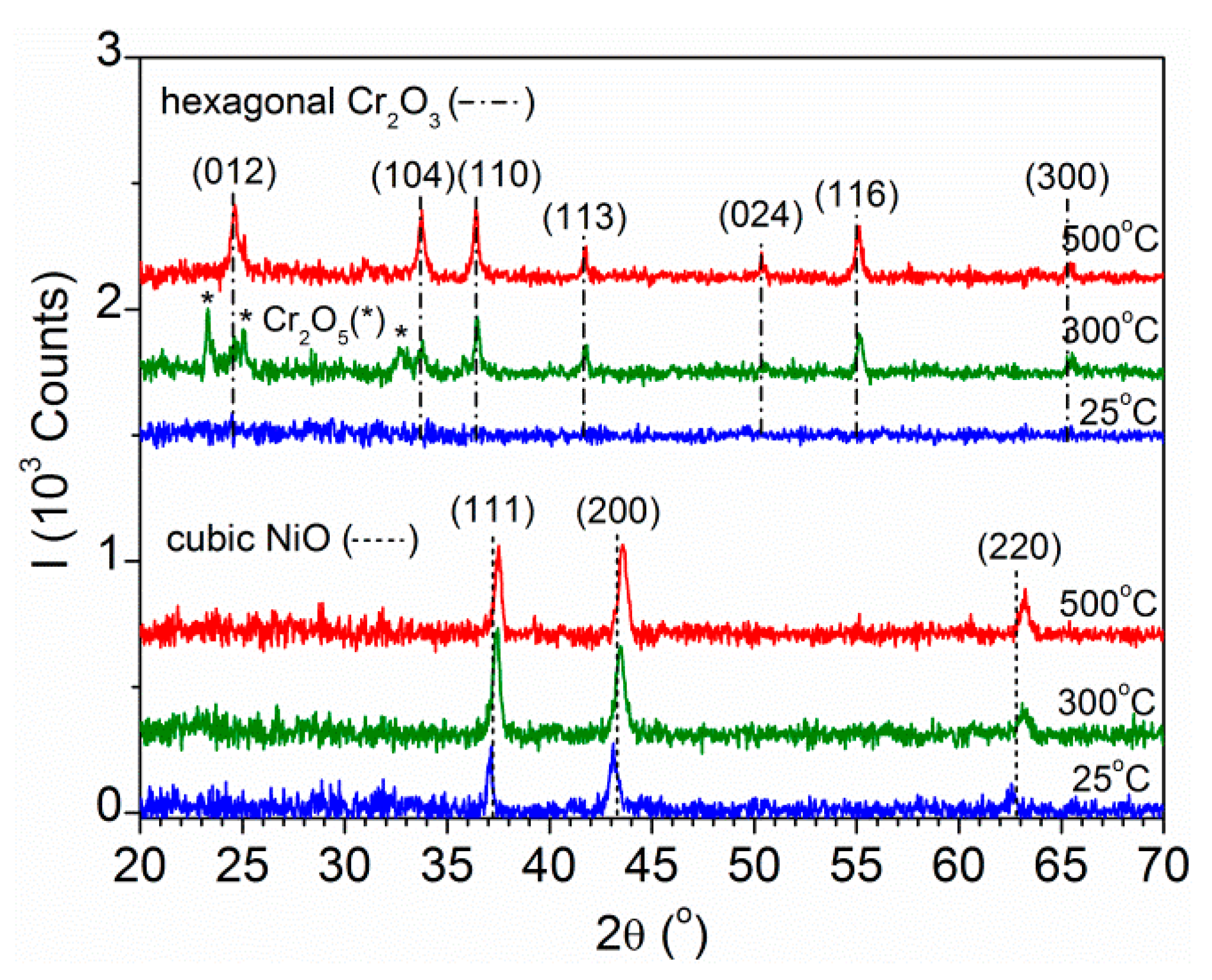
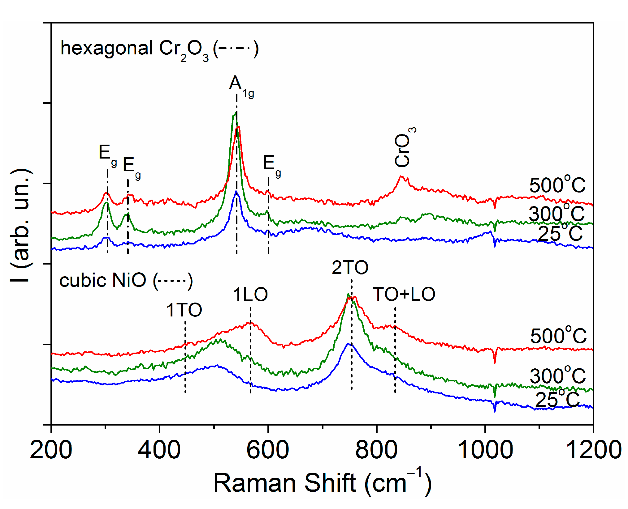
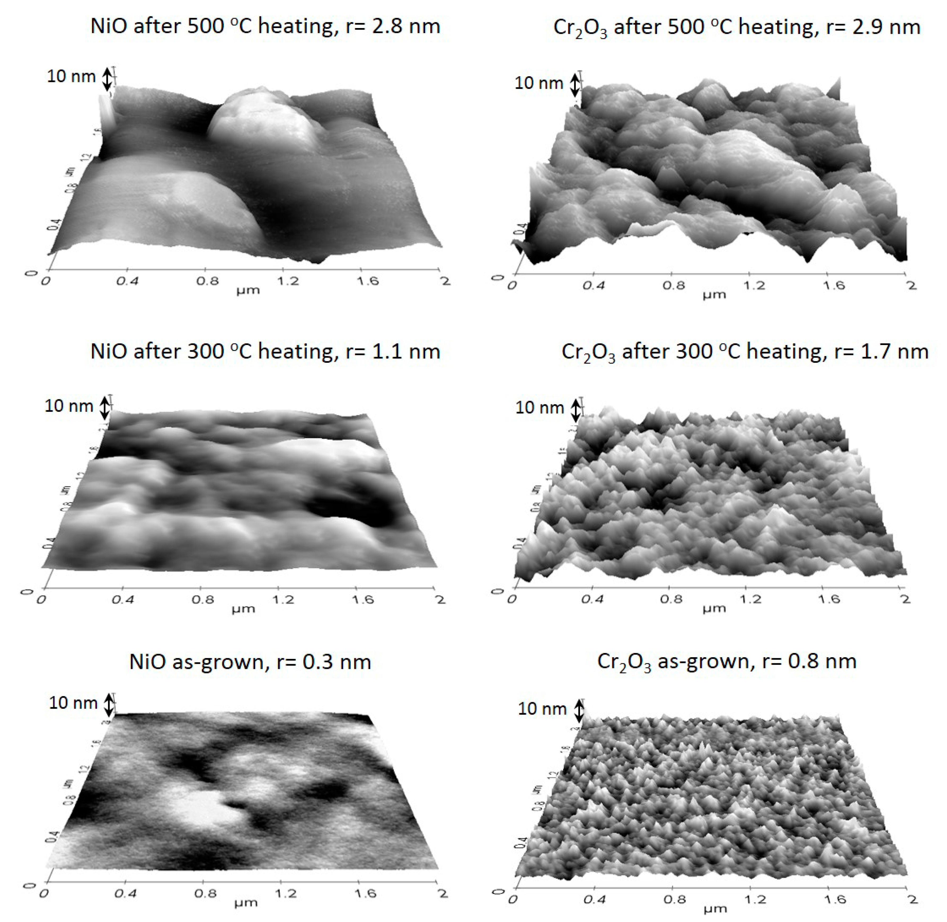
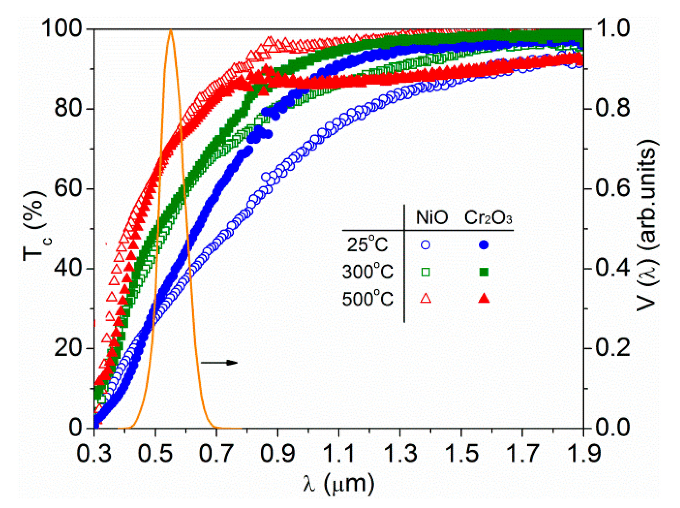
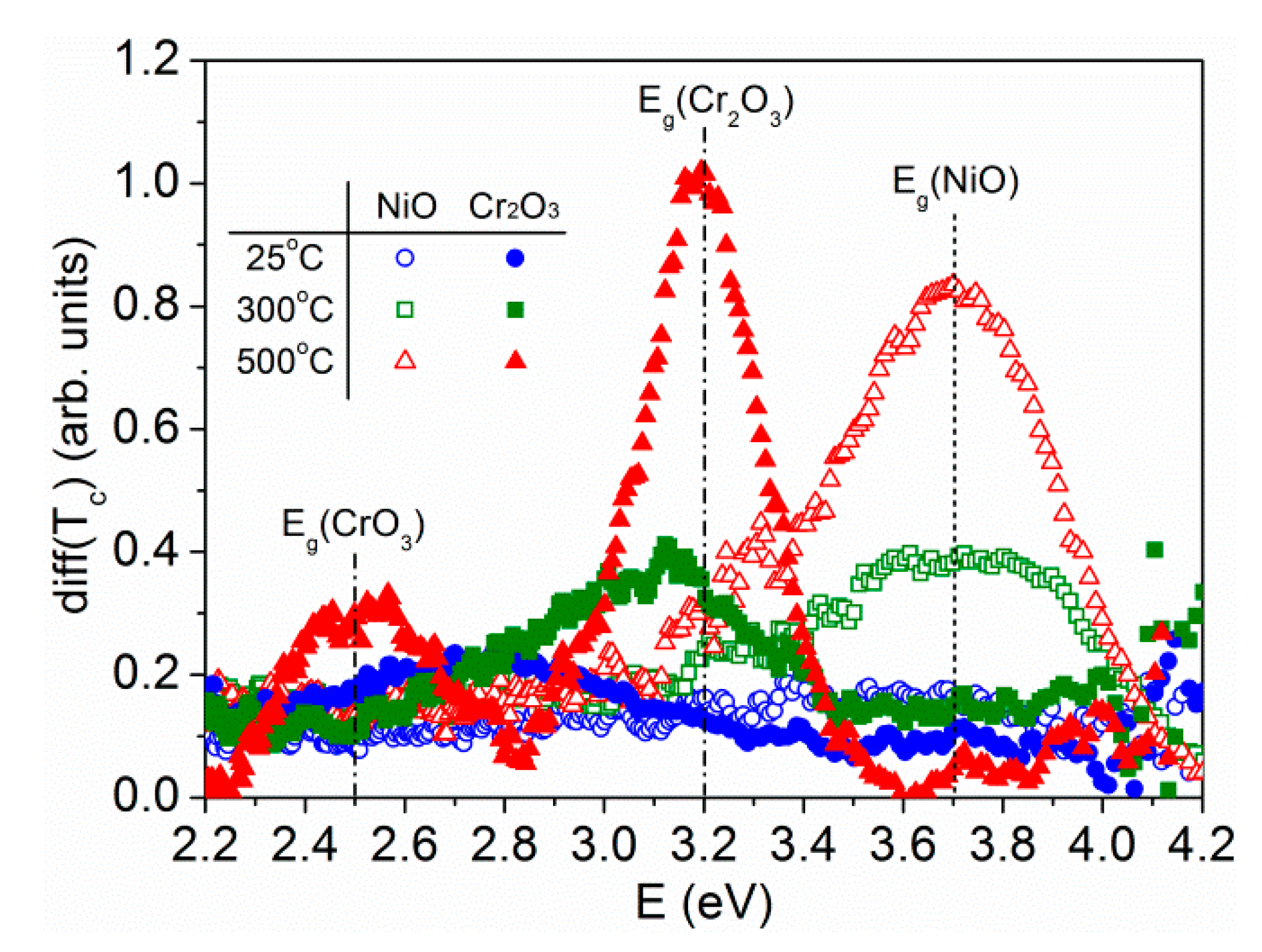
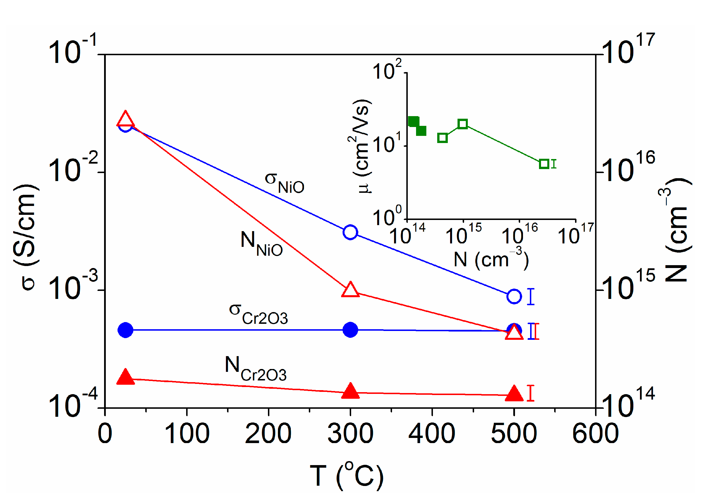
3. Results and Discussion
4. Conclusions
Author Contributions
Funding
Data Availability Statement
Acknowledgments
Conflicts of Interest
References
- Liu, L.; Cao, K.; Chen, S.; Huang, W. Toward see-through optoelectronics: Transparent light-emitting diodes and solar cells. Adv. Opt. Mater. 2020, 2001122, 1–31. [Google Scholar] [CrossRef]
- Morales-Masis, M.; De Wolf, S.; Woods-Robinson, R.; Ager, J.W.; Ballif, C. Transparent electrodes for efficient optoelectronics. Adv. Electron. Mater. 2017, 3. [Google Scholar] [CrossRef]
- Wang, Z.; Nayak, P.K.; Caraveo-Frescas, J.A.; Alshareef, H.N. Recent developments in p-type oxide semiconductor materials and devices. Adv. Mater. 2016, 28, 3831–3892. [Google Scholar] [CrossRef] [PubMed]
- Woods-Robinson, R.; Broberg, D.; Faghaninia, A.; Jain, A.; Dwaraknath, S.S.; Persson, K.A. Assessing high-throughput descriptors for prediction of transparent conductors. Chem. Mater. 2018, 30, 8375–8389. [Google Scholar] [CrossRef]
- Buckeridge, J.; Catlow, C.R.A.; Farrow, M.R.; Logsdail, A.J.; Scanlon, D.O.; Keal, T.W.; Sherwood, P.; Woodley, S.M.; Sokol, A.A.; Walsh, A. Deep vs shallow nature of oxygen vacancies and consequent n -type carrier concentrations in transparent conducting oxides. Phys. Rev. Mater. 2018, 2, 56–59. [Google Scholar] [CrossRef]
- Hu, L.; Wei, R.H.; Tang, X.W.; Lu, W.J.; Zhu, X.B.; Sun, Y.P. Design strategy for p-type transparent conducting oxides. J. Appl. Phys. 2020, 128, 140902. [Google Scholar] [CrossRef]
- Hu, L.; Zhao, M.L.; Liang, S.; Song, D.P.; Wei, R.H.; Tang, X.W.; Song, W.H.; Dai, J.M.; He, G.; Zhang, C.J.; et al. Exploring high-performance p-type transparent conducting oxides based on electron correlation in V2O3 thin films. Phys. Rev. Appl. 2019, 12, 1–9. [Google Scholar] [CrossRef]
- Yamaguchi, K.; Nakano, M.; Namimoto, H.; Fueno, T. Extended Hubbard models for transition metal oxides and halides: Importance of spin and charge fluctuations in charge transfer metals. Jpn. J. Appl. Phys. 1988, 27, L1835–L1838. [Google Scholar] [CrossRef]
- Shih, B.C.; Abtew, T.A.; Yuan, X.; Zhang, W.; Zhang, P. Screened Coulomb interactions of localized electrons in transition metals and transition-metal oxides. Phys. Rev. B-Condens. Matter Mater. Phys. 2012, 86, 1–8. [Google Scholar] [CrossRef]
- Fujimori, A.; Yoshida, T.; Okazaki, K.; Tsujioka, T.; Kobayashi, K.; Mizokawa, T.; Onoda, M.; Katsufuji, T.; Taguchi, Y.; Tokura, Y. Electronic structure of Mott-Hubbard-type transition-metal oxides. J. Electron Spectros. Relat. Phenomena 2001, 117–118, 277–286. [Google Scholar] [CrossRef]
- Zimmermann, R.; Steiner, P.; Claessen, R.; Reinert, F.; Hüfner, S.; Blaha, P.; Dufek, P. Electronic structure of 3d-transition-metal oxides: On-site Coulomb repulsion versus covalency. J. Phys. Condens. Matter 1999, 11, 1657–1682. [Google Scholar] [CrossRef]
- Guillén, C.; Herrero, J. Transparent and p-type conductive NixO:V thin films obtained by reactive DC sputtering at room temperature. Mater. Res. Express 2019, 6, 96410. [Google Scholar] [CrossRef]
- Mi, Z.; Chen, L.; Shi, C.; Ma, Y.; Wang, D.; Li, X.; Liu, H.; Qiao, L. The effects of strain and vacancy defects on the electronic structure of Cr2O3. Comput. Mater. Sci. 2018, 144, 64–69. [Google Scholar] [CrossRef]
- Hwang, J.D.; Ho, T.H. Effects of oxygen content on the structural, optical, and electrical properties of NiO films fabricated by radio-frequency magnetron sputtering. Mater. Sci. Semicond. Process. 2017, 71, 396–400. [Google Scholar] [CrossRef]
- Park, S.; Ahn, H.S.; Lee, C.K.; Kim, H.; Jin, H.; Lee, H.S.; Seo, S.; Yu, J.; Han, S. Interaction and ordering of vacancy defects in NiO. Phys. Rev. B Condens. Matter Mater. Phys. 2008, 77. [Google Scholar] [CrossRef]
- Medasani, B.; Sushko, M.L.; Rosso, K.M.; Schreiber, D.K.; Bruemmer, S.M. Vacancies and vacancy-mediated self diffusion in Cr2O3: A first-principles study. J. Phys. Chem. C 2017, 121, 1817–1831. [Google Scholar] [CrossRef]
- Tang, C.-J.; Ye, J.-M.; Yang, Y.-T.; He, J.-L. Large-area flexible monolithic ITO/WO3/Nb2O5/NiVOχ/ITO electrochromic devices prepared by using magnetron sputter deposition. Opt. Mater. 2016, 55, 83–89. [Google Scholar] [CrossRef]
- Egorova, K.S.; Ananikov, V.P. Toxicity of metal compounds: Knowledge and myths. Organometallics 2017, 36, 4071–4090. [Google Scholar] [CrossRef]
- Contoux, G.; Cosset, F.; Célérier, A.; Machet, J. Deposition process study of chromium oxide thin films obtained by d.c. magnetron sputtering. Thin Solid Films 1997, 292, 75–84. [Google Scholar] [CrossRef]
- Lin, J.; Sproul, W.D. Structure and properties of Cr2O3 coatings deposited using DCMS, PDCMS, and DOMS. Surf. Coat. Technol. 2015, 276, 70–76. [Google Scholar] [CrossRef]
- Hong, W.Q. Extraction of extinction coefficient of weak absorbing thin films from special absorption. J. Phys. D. Appl. Phys. 1989, 22, 1384–1385. [Google Scholar] [CrossRef]
- Garoufalis, C.S.; Barnasas, A.; Stamatelatos, A.; Karoutsos, V.; Grammatikopoulos, S.; Poulopoulos, P.; Baskoutas, S. A study of quantum confinement effects in ultrathin NiO films performed by experiment and theory. Materials 2018, 11, 949. [Google Scholar] [CrossRef]
- Miedzinska, K.M.E.; Hollebone, B.R.; Cook, J.G. Optical properties and assignment of the absorption spectra of sputtered mixed valence nickel oxide films. J. Phys. Chem. Solids 1988, 49, 1355–1362. [Google Scholar] [CrossRef]
- Mendoza-Galván, A.; Vidales-Hurtado, M.A.; López-Beltrán, A.M. Comparison of the optical and structural properties of nickel oxide-based thin films obtained by chemical bath and sputtering. Thin Solid Films 2009, 517, 3115–3120. [Google Scholar] [CrossRef]
- Zhu, M.; Li, F.; Zhou, G.; Jin, X.; Wang, X.; Wang, L.; Song, F. Microstructures and electrical properties of nanostructured Cr2O3 thin films deposited by dual-target reactive high-power impulse magnetron sputtering. Vacuum 2019, 164, 293–299. [Google Scholar] [CrossRef]
- Mohammadtaheri, M.; Yang, Q.; Li, Y.; Corona-Gomez, J. The effect of deposition parameters on the structure and mechanical properties of chromium oxide coatings deposited by reactive magnetron sputtering. Coatings 2018, 8, 111. [Google Scholar] [CrossRef]
- Abdullah, M.M.; Rajab, F.M.; Al-Abbas, S.M. Structural and optical characterization of Cr2O3 nanostructures: Evaluation of its dielectric properties. AIP Adv. 2014, 4. [Google Scholar] [CrossRef]
- Hewston, T.A.; Chamberland, B.L. Magnetic and structural studies of Cr2O5 and Cr3O8. J. Magn. Magn. Mater. 1984, 43, 89–95. [Google Scholar] [CrossRef]
- Ivanov, P.G.; Watts, S.M.; Lind, D.M. Epitaxial growth of CrO2 thin films by chemical-vapor deposition from a Cr8O21 precursor. J. Appl. Phys. 2001, 89, 1035–1040. [Google Scholar] [CrossRef]
- Si, P.Z.; Wang, H.X.; Jiang, W.; Lee, J.G.; Choi, C.J.; Liu, J.J. Synthesis, structure and exchange bias in Cr2O3/CrO2/Cr2O5 particles. Thin Solid Films 2011, 519, 8423–8425. [Google Scholar] [CrossRef]
- Gago, R.; Vinnichenko, M.; Hübner, R.; Redondo-Cubero, A. Bonding structure and morphology of chromium oxide films grown by pulsed-DC reactive magnetron sputter deposition. J. Alloys Compd. 2016, 672, 529–535. [Google Scholar] [CrossRef]
- Hones, P.; Diserens, M.; Lévy, F. Characterization of sputter-deposited chromium oxide thin films. Surf. Coat. Technol. 1999, 120–121, 277–283. [Google Scholar] [CrossRef]
- Dietz, R.E.; Parisot, G.I.; Meixner, A.E. Infrared absorption and Raman scattering by two-magnon processes in NiO. Phys. Rev. B 1971, 4, 2302–2310. [Google Scholar] [CrossRef]
- De Los Santos Valladares, L.; Ionescu, A.; Holmes, S.; Barnes, C.H.W.; Bustamante Domínguez, A.; Avalos Quispe, O.; González, J.C.; Milana, S.; Barbone, M.; Ferrari, A.C.; et al. Characterization of Ni thin films following thermal oxidation in air. J. Vac. Sci. Technol. B Nanotechnol. Microelectron. Mater. Process. Meas. Phenom. 2014, 32, 51808. [Google Scholar] [CrossRef]
- Ono, M.; Sasaki, K.; Nagai, H.; Yamaguchi, T.; Higashiwaki, M.; Kuramata, A.; Yamakoshi, S.; Sato, M.; Honda, T.; Onuma, T. Relation between electrical and optical properties of p-type NiO films. Phys. Status Solidi Basic Res. 2018, 255, 1–5. [Google Scholar] [CrossRef]
- Wang, M.; Thimont, Y.; Presmanes, L.; Diao, X.; Barnabé, A. The effect of the oxygen ratio control of DC reactive magnetron sputtering on as-deposited non stoichiometric NiO thin films. Appl. Surf. Sci. 2017, 419, 795–801. [Google Scholar] [CrossRef]
- Shim, S.H.; Duffy, T.S.; Jeanloz, R.; Yoo, C.S.; Iota, V. Raman spectroscopy and x-ray diffraction of phase transitions in Cr2O3 to 61 GPa. Phys. Rev. B-Condens. Matter Mater. Phys. 2004, 69, 1–12. [Google Scholar] [CrossRef]
- Barshilia, H.C.; Rajam, K.S. Growth and characterization of chromium oxide coatings prepared by pulsed-direct current reactive unbalanced magnetron sputtering. Appl. Surf. Sci. 2008, 255, 2925–2931. [Google Scholar] [CrossRef]
- Kikuchi, S.; Kawauchi, K.; Kurosawa, M.; Honjho, H.; Yagishita, T. Non-destructive rapid analysis discriminating between chromium(VI) and chromium(III) oxides in electrical and electronic equipment using Raman spectroscopy. Anal. Sci. 2005, 21, 197–198. [Google Scholar] [CrossRef]
- Monnereau, O.; Tortet, L.; Grigorescu, C.E.A.; Savastru, D.; Iordanescu, C.R.; Guinneton, F.; Notonier, R.; Tonetto, A.; Zhang, T.; Mihailescu, I.N.; et al. Chromium oxides mixtures in PLD films investigated by Raman spectroscopy. J. Optoelectron. Adv. Mater. 2010, 12, 1752–1757. [Google Scholar]
- Zhuang, S.; He, J.; Ma, X.; Zhao, Y.; Wang, H.; Zhang, B. Fabrication and optimization of hole transport layer NiO for all inorganic perovskite light emitting diodes. Mater. Sci. Semicond. Process. 2020, 109, 104924. [Google Scholar] [CrossRef]
- Keraudy, J.; García Molleja, J.; Ferrec, A.; Corraze, B.; Richard-Plouet, M.; Goullet, A.; Jouan, P.Y. Structural, morphological and electrical properties of nickel oxide thin films deposited by reactive sputtering. Appl. Surf. Sci. 2015, 357, 838–844. [Google Scholar] [CrossRef]
- Hotovy, I.; Huran, J.; Spiess, L. Characterization of sputtered NiO films using XRD and AFM. J. Mater. Sci. 2004, 39, 2609–2612. [Google Scholar] [CrossRef]
- Özen, S.; Şenay, V. Optical, morphological and nano-mechanical properties of chromium oxide thin films fabricated by radio frequency (RF) magnetron sputtering. Optik 2020, 201. [Google Scholar] [CrossRef]
- Yang, J.L.; Lai, Y.S.; Chen, J.S. Effect of heat treatment on the properties of non-stoichiometric p-type nickel oxide films deposited by reactive sputtering. Thin Solid Films 2005, 488, 242–246. [Google Scholar] [CrossRef]
- Atak, G.; Coşkun, Ö.D. Annealing effects of NiO thin films for all-solid-state electrochromic devices. Solid State Ionics 2017, 305, 43–51. [Google Scholar] [CrossRef]
- Singh, J.; Verma, V.; Kumar, R.; Kumar, R. Structural, optical and electrical characterization of epitaxial Cr2O3 thin film deposited by PLD. Mater. Res. Express 2019, 6, 106406. [Google Scholar] [CrossRef]
- Zhai, H.-J.; Li, S.; Dixon, D.A.; Wang, L.-S. Probing the electronic and structural properties of chromium oxide clusters (CrO3)n− and (CrO3)n ( n = 1–5): Photoelectron spectroscopy and density functional calculations. J. Am. Chem. Soc. 2008, 130, 5167–5177. [Google Scholar] [CrossRef] [PubMed]
- Makhlouf, S.A.; Kassem, M.A.; Abdel-Rahim, M.A. Crystallite size-dependent optical properties of nanostructured NiO films. Optoelectron. Adv. Mater. Rapid Commun. 2010, 4, 1562–1568. [Google Scholar]
- Ekwealor, A.B.C. Variations of optical and structural properties with temperature for CrxOy thin films synthesized in a polymer matrix by chemical bath deposition technique. Dig. J. Nanomater. Biostruct. 2014, 9, 423–431. [Google Scholar]
- Kucheyev, S.O.; Sadigh, B.; Baumann, T.F.; Wang, Y.M.; Felter, T.E.; van Buuren, T.; Gash, A.E.; Satcher, J.H.; Hamza, A.V. Electronic structure of chromia aerogels from soft X-ray absorption spectroscopy. J. Appl. Phys. 2007, 101, 124315. [Google Scholar] [CrossRef]
- Karsthof, R.; Anton, A.M.; Kremer, F.; Grundmann, M. Nickel vacancy acceptor in nickel oxide: Doping beyond thermodynamic equilibrium. Phys. Rev. Mater. 2020, 4, 1–9. [Google Scholar] [CrossRef]
- Singh, J.; Kumar, R.; Verma, V.; Kumar, R. Structural and optoelectronic properties of epitaxial Ni-substituted Cr2O3 thin films for p-type TCO applications. Mater. Sci. Semicond. Process. 2020, 105483. [Google Scholar] [CrossRef]
- Bosman, A.J.; van Daal, H.J. Small-polaron versus band conduction in some transition-metal oxides. Adv. Phys. 1970, 19, 1–117. [Google Scholar] [CrossRef]


| Target (Ø 15 cm) | Pbase (Pa) | P(O2) (Pa) | P(O2 + Ar) (Pa) | Power (W/cm2) |
|---|---|---|---|---|
| Ni disk | 4 × 10⁻⁴ | 0.10 | 0.50 | 2 |
| Cr disk | 4 × 10⁻⁴ | 0.20 | 0.50 | 12 |
Publisher’s Note: MDPI stays neutral with regard to jurisdictional claims in published maps and institutional affiliations. |
© 2021 by the authors. Licensee MDPI, Basel, Switzerland. This article is an open access article distributed under the terms and conditions of the Creative Commons Attribution (CC BY) license (http://creativecommons.org/licenses/by/4.0/).
Share and Cite
Guillén, C.; Herrero, J. Structural Changes Induced by Heating in Sputtered NiO and Cr2O3 Thin Films as p-Type Transparent Conductive Electrodes. Electron. Mater. 2021, 2, 49-59. https://doi.org/10.3390/electronicmat2020005
Guillén C, Herrero J. Structural Changes Induced by Heating in Sputtered NiO and Cr2O3 Thin Films as p-Type Transparent Conductive Electrodes. Electronic Materials. 2021; 2(2):49-59. https://doi.org/10.3390/electronicmat2020005
Chicago/Turabian StyleGuillén, Cecilia, and José Herrero. 2021. "Structural Changes Induced by Heating in Sputtered NiO and Cr2O3 Thin Films as p-Type Transparent Conductive Electrodes" Electronic Materials 2, no. 2: 49-59. https://doi.org/10.3390/electronicmat2020005
APA StyleGuillén, C., & Herrero, J. (2021). Structural Changes Induced by Heating in Sputtered NiO and Cr2O3 Thin Films as p-Type Transparent Conductive Electrodes. Electronic Materials, 2(2), 49-59. https://doi.org/10.3390/electronicmat2020005