Abstract
Inkjet-printed patterns were formed on a paper substrate using anti-oxidant copper nano-ink for application to disposable electronic devices. To prevent substrate damage, the pattern was flash light sintered under ambient conditions using the multi-pulse technique. Pure copper nanoparticles were coated with 1-octanethiol for oxidation resistance using the dry-coating method. Mixing these with 1-octanol solvent at a concentration of 30 wt% produced the copper nano-ink. Photo paper was used as the substrate. The contact angle between the photo paper and copper nano-ink was 37.2° and the optimal energy density for the multi-pulse flash light sintering technique was 15.6 J/cm2. Using this energy density, the optimal conditions were an on-time of 2 ms (duty cycle of 80%) for three pulses. The resistivity of the resulting pattern was 2.8 × 10⁻⁷ Ω∙m. After bending 500 times to a radius of curvature of 30 mm, the relative resistance (ΔR/R0) of the multi-pulse flash light-sintered pattern hardly changed compared to that of the unbent pattern, while the single-pulse-sintered pattern showed dramatic increase by 8-fold compared to the unbent pattern. Therefore, the multi-pulse light sintering technique is a promising approach to produce an inkjet-printed pattern that can be applied to disposable electronic devices.
1. Introduction
Recently, many studies have focused on flexible electronic devices with flexible substrates [1]. Flexible substrates have various advantages, such as being light weight and easy to fabricate due to their plasticity [2,3,4,5]. In particular, paper, a low-cost flexible substrate, decomposes without producing harmful materials and is suitable for application to disposable electronic devices [6,7]. Moreover, this substrate has the advantage of being suited to printed electronics [8,9,10,11]. Therefore, many studies have used the inkjet printing method to fabricate paper electronic materials [12,13]. Various metal nano-inks [14] have been applied via methods such as non-contact deposition to flexible substrates; this is called the “drop-on-demand” method [15,16,17]. Inkjet printing is cheap, environmentally friendly, and easy to apply in the roll-to-roll industry [18]. Recently, the inkjet printing method has been extensively studied for application in the fields of e-paper [19,20], and smart packaging [21]. This method typically uses noble metal ink, such as gold or silver [22], which has high electrical conductivity but is expensive. Many studies have focused on copper due to its high ratio of electrical conductivity to price [23,24]; however, copper powders are prone to oxidation [25].
Our previous study developed an ultra-thin organic coating for vapor self-assembled multilayers made of an alkanethiol material, 1-octanethiol, for the surface of pure Cu nanopowder to prevent oxidation [26,27,28]. The coated nanoparticles were fabricated with solvent and the study optimized the conditions to form them into copper nano-ink [29]. After patterning, the pattern was needed for sintering process to remove any solvent residues. The light sintering method has been studied extensively due to its electrical performance being better than that of heat furnace sintering [30,31,32,33]. Light sintering is achieved by irradiating substrates with high-energy photons in pulses with a short duration as shown in Figure S1 [34,35]. Recently, the multi-pulse flash light sintering technique has been drawing attention in the field of flexible electronics due to its good sintering properties [36]. In this study, we patterned inkjet-printed ink on a paper substrate using anti-oxidant copper nano-ink. Moreover, we used flash light sintering with the multi-pulse technique to enhance the electrical conductivity on a low-cost, paper substrate.
2. Experimental Process
2.1. Fabrication of Copper Nano-Ink Using 1 Octanethiol-Coated Cu Nanoparticles
We synthesized 100 nm-scale copper nanoparticles using the polyol method. To remove the residual polyvinylpyrrolidone and diethylene glycol, pure methanol and a toluene solvent were used for washing. The washing process was completed five times. Next, polyvinylpyrrolidone-free copper nanoparticles were coated under high vacuum (4.0 × 10⁻⁶ torr) using 1-octanethiol solvent [28,29].
The coated copper nanoparticles were mixed with 1-octanol solvent and sonicated for 30 min at room temperature to make 30 wt% copper nano-ink. Photo paper (semigloss; EPSON, Suwa City, Japan) based on cellulose with a thickness of 263 μm (Figure S2) was used for the substrate.
2.2. Inkjet Printing Followed by Flash Light Sintering
1-Octanethiol-coated copper nano-ink was printed on the paper substrate using an inkjet printer (DMP-2831; Dimatix, Santa Clara, CA, USA). Sixteen nozzles were used, with a drop spacing of 20 μm (1270 dpi). Jetting voltage was 32 V at a temperature of 40 °C. The length and width of the pattern were 10 and 5 mm, respectively. The length and width of the sample used for a bending test were 10 and 1 mm, respectively. The printed patterns dried at room temperature.
Flash light sintering was conducted using a system (IPL-45kW_2100; PS Tek, Gunpo-si, Gyeonggi-do, Korea) with an energy density of 15.6 J/cm2. A xenon lamp was used for the light source, and the distance between it and the substrate was 43 mm. Energy densities for all conditions were measured using an illuminometer (NOVA II; OPHIR Photonics Group, North Logan, UT, USA). Compared to conventional light sintering, single-pulse flash light sintering is defined as having a higher peak power for a shorter time. Multi-pulse flash light sintering was conducted with on-times of 1, 2, and 3 ms, with duty cycles calculated to be 67%, 80%, and 86%, respectively, under the same energy density but differing peak power, as explained in the Figure S3. The copper pattern used for flash light sintering had a thickness of 1.2 μm. The contact angle was measured using a contact angle analyzer (Phoenix 300; Kromtek, Dubai, United Arab Emirates) while the thickness of the copper pattern and its resistivity were measured using probes (Alpha-Step and 4 point, respectively).
3. Results
3.1. Single-Step Flash Light Sintering
The copper pattern was sintered using white light at an energy density of 15.6 J/cm2 with a single pulse in one step; the experimental conditions are summarized in Table 1. This single-step sintering process was conducted with two sets of parameters. First, a single pulse of 4-ms duration and 1.3-MW peak power was used. Then, a single pulse of 16 ms duration and 0.285 MW peak power was used. The pattern resistivity under the first conditions was 5.4 × 10⁻⁵ Ω∙m with a relatively large standard deviation (Figure 1a). However, the resistivity was not measured under the second set of conditions due to incomplete sintering of the copper pattern. Observation of the microstructure of the pattern confirmed the resistivity trend: under the conditions of 4 ms and 1.3 MW, the Cu surface seemed to be sintered, with a necking structure among the copper nanoparticles (Figure 1b,c). However, for the case of 16 ms and 0.285 MW, it was observed that Cu nanoparticles did not form any necking. Based on these observations, we concluded that the single-pulse conditions varying peak power and time, under the same energy density, seem to be unsuitable for sintering on the paper substrate.

Table 1.
Single-pulse flash light sintering conditions.
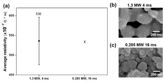
Figure 1.
Average resistivity and microstructural observation results of Cu printed patterns after single-step flash light sintering: (a) comparison of average resistivities for two sets of single-pulse sintering conditions, and scanning electron microscope images for conditions of (b) 1.3 MW and 4 ms, and (c) 0.285 MW and 16 ms.
3.2. Multi-Step Flash Light Sintering with the Same Energy Density
The paper substrate had low thermal conductivity; therefore, it needed sufficient time to cool to prevent a drastic increase in temperature. To overcome this problem, the copper pattern was sintered via multi-step flash light sintering under the same energy density of 15.6 J/cm2 as optimized in Figure S4. This technique prevented a drastic temperature increase and allowed successful fabrication of the copper pattern.
3.2.1. Multi Step Sintering under Various Duty Cycle
As shown in Table 2, the sintering conditions were varied by cooling time, with a duty cycle calculated for each set of conditions under a constant peak power of 0.93 MW. A duty cycle of 80% gave the lowest resistivity value, indicating that the optimal cooling time was 0.5 ms (Figure 2a). The microstructure appeared as we would expect from the resistivity trend, with that for the 80% duty cycle exhibiting a high density of copper nanoparticles (Figure 2c). By contrast, scanning electron microscope images for duty cycles of 100% and 50% showed many pores among the sintered nanoparticles. Accordingly, the optimal condition included a duty cycle of 80%. As shown in Figure 2b, the temperature increased with duty cycle. The temperature measured for the optimal duty cycle was 114 °C, which was a little lower than with conventional heat sintering technology. This can be explained by the heat dissipation, as discussed in the following section.
Table 2.
Multi-pulse sintering conditions with various duty cycles.
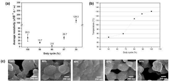
Figure 2.
Sintering results for various duty cycles under the same energy density of 15.6 J/cm2: (a) copper pattern resistivity, (b) microstructure, and (c) temperature.
3.2.2. Calculating Heat Dissipation
Using the equations below,
- Qin, out: Heat transferred to the fluid (J);
- q: Object density (kg/cm3);
- V: Object volume (m3);
- Cp,v: Heat capacity (J/kg∙K);
we calculated the heat consumption for the paper substrate, which may explain the lower temperature found with the multi-pulse sintering. Our study used the transient heat transfer model, which can calculate the amount of convective cooling or heating using each material’s heat capacity (Table 3). The results of these calculations are presented in Table 4. For an energy density of 15.6 J/cm2, the energy dissipated as heat was calculated to be 0.22−0.34 J, showing that almost all the heat was dissipated via the copper pattern. However, the substrate temperature also changed during sintering, so the real values would be lower than these. Note that Qin increased with duty cycle.
Table 3.
Heat capacity (C) and density (ρ) of copper and paper.
Table 4.
Heat dissipation calculation results.
3.2.3. Effect of Varying Multi-Pulse Time
We conducted multi-step sintering with various sintering times by varying the number of pulses using the same energy density of 15.6 J/cm2, on-time of 1 ms, and duty cycle of 67% (Table 5). The lowest resistivity value of 3.8 × 10⁻⁷ Ω∙m was obtained with eight pulses (Figure 3a). As shown in Figure 3b, eight pulses also gave the best necking structure among the copper nanoparticles. By contrast, there were some pores in the surface for all other numbers of pulses; this microstructure explains why the resistivity value was highest for eight pulses.
Table 5.
Multi-pulse sintering conditions with various sintering times (each pulse lasted 1 ms).
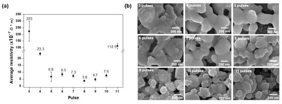
Figure 3.
Results of multi-pulse sintering for various sintering times under the same energy density of 15.6 J/cm2 with a pulse on-time of 1 ms: (a) resistivity measurements and (b) scanning electron microscope images.
To improve the electrical resistivity, our next step was to increase the sintering time to better induce the densified necking structure. We used a sintering on-time of 2 ms, giving a duty cycle of 80%, and measured the resistivity after 2−6 pulses (Table 6). Resistivity increased with the number of pulses with three pulses giving the lowest resistivity of 2.8 × 10⁻⁷ Ω∙m (Figure 4a) compared to its resistivity of 1.68 × 10⁻⁸ Ω∙m for the bulk Copper [37]. As before, the corresponding scanning electron microscope image showed densified structure of the copper nanoparticles (Figure 4b). When the peak power rose above 0.93 MW for more than three pulses, more pores appeared in the structure. For a peak power lower than 0.93 MW, the microstructure showed an incomplete sintering microstructure.
Table 6.
Multi-pulse sintering condition (each pulse 2 ms).
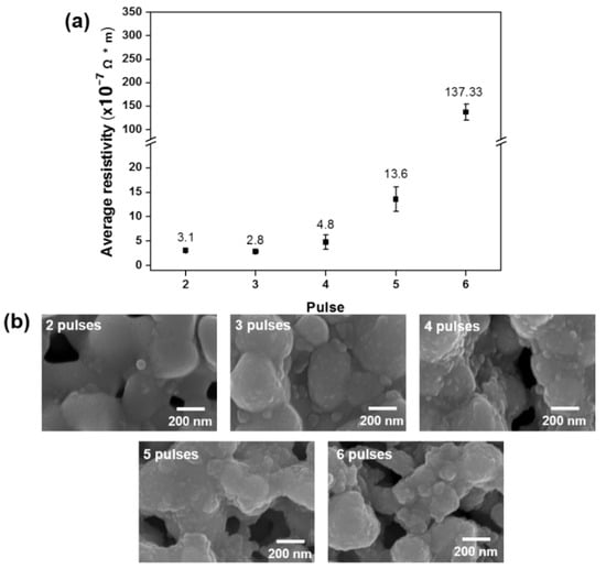
Figure 4.
Results of multi-pulse sintering for various sintering times under the same energy density of 15.6 J/cm2 with a pulse on-time of 2 ms: (a) resistivity measurements and (b) scanning electron microscope images.
To improve the resistivity, we increased the sintering on-time to 3 ms, with conditions listed in Table 7. As shown in Figure 5a, the value of the measured resistivities were relatively higher than those in Figure 3a and Figure 4a. The microstructures also showed many pores on the copper pattern surface (Figure 5b). Therefore, multi-pulse sintering has a set of optimal conditions for the duty cycle and number of pulses. When the duty cycle (or on-time) and number of pulses differed from these, the resistivity of the copper pattern was higher. Thus, under the same energy density, the most important parameters are sintering time and peak power.
Table 7.
Multi-pulse sintering condition (each pulse 3 ms).
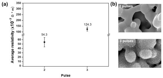
Figure 5.
Results of multi-pulse sintering for various sintering times under the same energy density of 15.6 J/cm2 with a pulse on-time of 3 ms: (a) resistivity measurements and (b) scanning electron microscope images.
3.2.4. Analysis of Patterns Produced Using the Optimal Multi-Pulse Parameters
We used the optimal parameters to produce patterns on paper and polyimide substrates and we compared these quantitatively by X-ray photoelectron spectroscopy analysis (Figure 6a). The elements detected were carbon, copper, sulfur, and oxygen. The copper pattern on the paper substrate contained more sulfur and oxygen than that on the polyimide (Kolon, Nanjing, China) substrate. The resistivities of these patterns were 8.3 × 10⁻⁸ and 2.8 × 10⁻⁷ Ω∙m on the polyimide and paper, respectively. The difference was due to the two different energy densities we used; that used on the polyimide substrate was twice that used on the paper substrate, suggesting that sintering at a higher energy density easily removes sulfur and oxygen as XPS analysis confirms absence of Cu-S bonding shown in Figure S5. In contrast, the copper pattern on the paper substrate still had CuS on its surface (Figure 6b). As shown in Table 8, CuS has higher resistivity than pure copper under the same sintering conditions [38,39]; therefore, the remaining CuS has higher resistivity. Cross-sectional images showed that the copper nanoparticles had not fully densified, resulting in a higher resistivity than for bulk copper (Figure 6c).
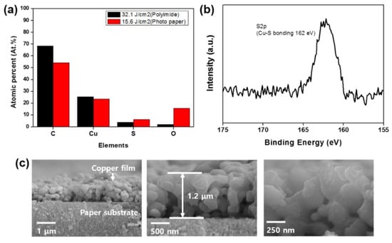
Figure 6.
Results from sintering with optimal multi-pulse parameters under two energy densities (32.1 and 15.6 J/cm2) on two surfaces (polyimide and photo paper, respectively) using X-ray photoelectron spectroscopy: (a) proportions of elements, (b) peak (at 162 eV) showing that Cu−S bonds remained at the surface, and (c) cross-sectional scanning electron microscope images of the paper substrate.
Table 8.
Resistivities of copper and copper sulfide at the same sintering temperature.
3.3. Bending Properties of the Copper Pattern on Paper Substrate
We used the optimal conditions for single-pulse (1.3 MW, 4 ms) and multi-pulse sintering (2 ms, three pulses, duty cycle of 80%) to produce patterns whose bending properties were evaluated for a radius of curvature of 30 mm. The relative resistance of the single-pulse sintered pattern increased after bending 100 times, and exhibited dramatic increase in relative resistance of eight compared to the unbent pattern after 500 bending cycles (Figure 7a). By contrast, the relative resistance of the multi-pulse sintered pattern increased by only 0.6. This result can be explained by the porous structure; the microstructure of the single-pulse sintered pattern had many pores on the copper surface which can propagate cracks (Figure 1b), thereby causing the increase in the relative resistance. A copper pattern successfully fabricated on the paper substrate using multi-pulse sintering under the optimal conditions is shown in Figure 7b.
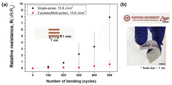
Figure 7.
(a) Relative resistances of patterns produced by single- and multi-pulse sintering under their optimal conditions and (b) photograph of the multi-pulse sintered pattern.
3.4. The Characteristic of Multi-Pulse Sintering
When a single pulse irradiates a copper pattern, it induces the photothermal effect causing an increase in temperature (Figure 8a). With a paper substrate, the heat cannot diffuse due to its low thermal conductivity (Table 9). Therefore, the heat remains in the copper pattern, causing a drastic temperature increase, and inducing local sintering there. As a result, there are many pores on the copper pattern surface. By contrast, multi-pulse sintering gave a different result due to the more favorable peak power and cooling time. When a photon enters the copper pattern there is a temperature increase due to the photothermal effect; however, the more favorable peak power does not induce a drastic temperature increase and the cooling time allows the temperature to drop again. Therefore, the copper pattern achieved a reasonable temperature in the flash sintering process. This phenomenon induced a gradual temperature increase, helping to densify the structure of the copper pattern [40,41]. The flash light sintering mechanism can provide a range of reasonable sintering conditions based on the values for peak power and time that we used (Figure 8b).
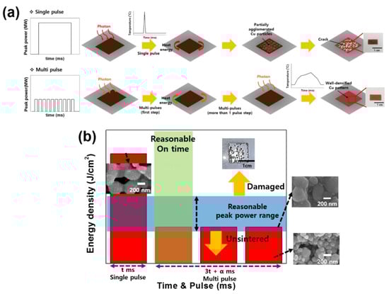
Figure 8.
(a) Mechanisms of single- and multi-step sintering, and (b) diagram of strategy for finding the optimal flash sintering conditions under the same energy density.
Table 9.
Thermal conductivities of various substrates.
4. Conclusions
To fabricate flexible and disposable electronics successfully, this study conducted a flash light sintering process on a paper substrate. We measured the electrical conductivity and durability of the copper patterns formed under the same energy density (15.6 J/cm2). To improve on single-step flash sintering, we conducted multi-step sintering under varied conditions, such as duty cycle and number of pulses. The optimal conditions were a duty cycle of 80% at 2 ms with three pulses, achieving a resistivity of 2.8 × 10⁻⁷ Ω∙m. Multi-pulse sintering gave better quality than single-pulse sintering under the same energy density. Under the bending test of 500 times, the relative resistance of the multi-pulse sintered copper pattern hardly changed compared to the unbent pattern while the single-pulse sintered pattern showed dramatic increase in its relative resistance by 8-fold compared to that of the unbent pattern. Therefore, we successfully fabricated a copper pattern on a paper substrate which presents possibilities for developing disposable electronic devices.
Supplementary Materials
The following are available online at https://www.mdpi.com/2673-3978/1/1/4/s1, Figure S1: (a) Flash light sintering process and (b) relationship of energy density to peak power and time. Figure S2: (a) Photo paper surface, (b) cross-sectional image, and (c) contact angle between the substrate and copper nano-ink. Figure S3: Relationship between duty cycle, on-time, and off-time. Figure S4: Results of multi-pulse sintering for various energy densities under the same condition with varying pulses: (a) resistivity measurements and (b) scanning electron microscope images. Figure S5: X-ray photoelectron spectroscopy of multi-pulse light-sintered, inkjet-printed copper pattern on PI substrate under the energy density of 32.1 J/cm2.
Author Contributions
Writing—original draft preparation, Y.S., C.S.L.; Writing—review and editing, D.S., C.S.L.; Resources, Writing—review and editing, M.K.; Supervision, C.S.L. All authors have read and agreed to the published version of the manuscript.
Funding
This work was supported by grant funded by the National Research Foundation (NRF) of Korea grant funded by government (MSIT) (No. 2019R1F1A1060586) and ONSEM Semiconductor project.
Conflicts of Interest
The authors declare no conflict of interest.
References
- Eda, G.; Fanchini, G.; Chhowalla, M. Large-area ultrathin films of reduced graphene oxide as a transparent and flexible electronic material. Nat. Nanotechnol. 2008, 3, 270–274. [Google Scholar] [CrossRef]
- Mastrototaro, J.J.; Johnson, K.W.; Morff, R.J.; Lipson, D.; Andrew, C.C.; Allen, D.J. An electroenzymatic glucose sensor fabricated on a flexible substrate. Sens. Actuators B Chem. 1991, 5, 139–144. [Google Scholar] [CrossRef]
- Yu, T.; Ni, Z.; Du, C.; You, Y.; Wang, Y.; Shen, Z. Raman mapping investigation of graphene on transparent flexible substrate: The strain effect. J. Phys. Chem. C 2008, 112, 12602–12605. [Google Scholar] [CrossRef]
- Matsuhisa, N.; Kaltenbrunner, M.; Yokota, T.; Jinno, H.; Kuribara, K.; Sekitani, T.; Someya, T. Printable elastic conductors with a high conductivity for electronic textile applications. Nat. Commun. 2015, 6, 7461. [Google Scholar] [CrossRef] [PubMed]
- Luo, H.; Wang, C.; Linghu, C.; Yu, K.; Wang, C.; Song, J. Laser-driven programmable non-contact transfer printing of objects onto arbitrary receivers via an active elastomeric microstructured stamp. Natl. Sci. Rev. 2020, 7, 296–304. [Google Scholar] [CrossRef]
- Pais, A.; Banerjee, A.; Klotzkin, D.; Papautsky, I. High-sensitivity, disposable lab-on-a-chip with thin-film organic electronics for fluorescence detection. Lab. Chip 2008, 8, 794–800. [Google Scholar] [CrossRef]
- Gadsby, P.D.; Moore, M.R.; Olson, D.E.; Scott, B.M. Disposable biopotential electrode. U.S. Patent 4,852,571, 1 August 1989. [Google Scholar]
- Hyun, W.J.; Secor, E.B.; Hersam, M.C.; Frisbie, C.D.; Francis, L.F. High-resolution patterning of graphene by screen printing with a silicon stencil for highly flexible printed electronics. Adv. Mater. 2015, 27, 109–115. [Google Scholar] [CrossRef]
- Gaikwad, A.M.; Steingart, D.A.; Nga Ng, T.; Schwartz, D.E.; Whiting, G.L. A flexible high potential printed battery for powering printed electronics. Appl. Phys. Lett. 2013, 102, 104_1. [Google Scholar] [CrossRef]
- Zhou, H.; Qin, W.; Yu, Q.; Cheng, H.; Yu, X.; Wu, H. Transfer Printing and its Applications in Flexible Electronic Devices. Nanomaterials 2019, 9, 283. [Google Scholar] [CrossRef]
- Linghu, C.; Zhang, S.; Wang, C.; Song, J. Transfer printing techniques for flexible and stretchable inorganic electronics. NPJ Flex. Electron. 2018, 2, 26. [Google Scholar] [CrossRef]
- Yang, L.; Rida, A.; Vyas, R.; Tentzeris, M.M. RFID tag and RF structures on a paper substrate using inkjet-printing technology. IEEE Trans. Microw. Theory Tech. 2007, 55, 2894–2901. [Google Scholar] [CrossRef]
- Shaker, G.; Safavi-Naeini, S.; Sangary, N.; Tentzeris, M.M. Inkjet printing of ultrawideband (UWB) antennas on paper-based substrates. IEEE Antennas Wirel. Propag. Lett. 2011, 10, 111–114. [Google Scholar] [CrossRef]
- Kim, S.; Lee, W.S.; Lee, J.; Park, I. Direct micro/nano metal patterning based on two-step transfer printing of ionic metal nano-ink. Nanotechnology 2012, 23, 285301. [Google Scholar] [CrossRef] [PubMed]
- Sirringhaus, H.; Kawase, T.; Friend, R.; Shimoda, T.; Inbasekaran, M.; Wu, W.; Woo, E. High-resolution inkjet printing of all-polymer transistor circuits. Science 2000, 290, 2123–2126. [Google Scholar] [CrossRef]
- Calvert, P. Inkjet printing for materials and devices. Chem. Mater. 2001, 13, 3299–3305. [Google Scholar] [CrossRef]
- Shrestha, M.; Lu, Z.; Lau, G.-K. Transparent Tunable Acoustic Absorber Membrane Using Inkjet-Printed PEDOT:PSS Thin-Film Compliant Electrodes. ACS Appl. Mater. Interfaces 2018, 10, 39942–39951. [Google Scholar] [CrossRef]
- Krebs, F.C.; Gevorgyan, S.A.; Alstrup, J. A roll-to-roll process to flexible polymer solar cells: Model studies, manufacture and operational stability studies. J. Mater. Chem. 2009, 19, 5442–5451. [Google Scholar] [CrossRef]
- Moberg, Å.; Johansson, M.; Finnveden, G.; Jonsson, A. Printed and tablet e-paper newspaper from an environmental perspective—A screening life cycle assessment. Environ. Impact Assess. Rev. 2010, 30, 177–191. [Google Scholar] [CrossRef]
- Park, J.-H.; Lee, J.-H.; Kim, D.; Hwang, K.-T.; Kim, J.-H.; Han, K.-S. Ink-Jet 3D Printability of Ceramic Ink with Contact Angle Control. J. Korean Ceram. Soc. 2019, 56. [Google Scholar] [CrossRef]
- Kuswandi, B.; Wicaksono, Y.; Abdullah, A.; Heng, L.Y.; Ahmad, M. Smart packaging: Sensors for monitoring of food quality and safety. Sens. Instrum. Food Qual. Saf. 2011, 5, 137–146. [Google Scholar] [CrossRef]
- Lee, H.-H.; Chou, K.-S.; Huang, K.-C. Inkjet printing of nanosized silver colloids. Nanotechnology 2005, 16, 2436. [Google Scholar] [CrossRef] [PubMed]
- Joo, S.-J.; Hwang, H.-J.; Kim, H.-S. Highly conductive copper nano/microparticles ink via flash light sintering for printed electronics. Nanotechnology 2014, 25, 265601. [Google Scholar] [CrossRef] [PubMed]
- Yu, J.H.; Kang, K.-T.; Hwang, J.Y.; Lee, S.-H.; Kang, H. Rapid sintering of copper nano ink using a laser in air. Int. J. Precis. Eng. Manuf. 2014, 15, 1051–1054. [Google Scholar] [CrossRef]
- Li, J.; Mayer, J.; Colgan, E. Oxidation and protection in copper and copper alloy thin films. J. Appl. Phys. 1991, 70, 2820–2827. [Google Scholar] [CrossRef]
- Kwon, J.; Park, S.; Haque, M.; Kim, Y.-S.; Lee, C.S. Study of Sintering Behavior of Vapor Forms of 1-Octanethiol Coated Copper Nanoparticles for Application to Ink-Jet Printing Technology. J. Nanosci. Nanotechnol. 2012, 12, 3434–3437. [Google Scholar] [CrossRef] [PubMed]
- Her, J.; Cho, D.; Lee, C.S. Synthesis of conductive nano ink using 1-octanethiol coated copper nano powders in 1-octanol for low temperature sintering process. Mater. Trans. 2013, 54, 599–602. [Google Scholar] [CrossRef]
- Kwon, J.; Park, S.; Lee, T.H.; Yang, J.-M.; Lee, C.S. Investigation of oxidation inhibition properties of vaporized self-assembled multilayers on copper nanopowders. Appl. Surf. Sci. 2011, 257, 5115–5120. [Google Scholar] [CrossRef]
- Cho, D.; Baik, J.-H.; Choi, D.-H.; Lee, C.S. Dispersion stability of 1-octanethiol coated Cu nanoparticles in a 1-octanol solvent for the application of nanoink. Appl. Surf. Sci. 2014, 309, 300–305. [Google Scholar] [CrossRef]
- Hwang, H.-J.; Chung, W.-H.; Kim, H.-S. In situ monitoring of flash-light sintering of copper nanoparticle ink for printed electronics. Nanotechnology 2012, 23, 485205. [Google Scholar] [CrossRef] [PubMed]
- Chung, W.-H.; Hwang, H.-J.; Lee, S.-H.; Kim, H.-S. In situ monitoring of a flash light sintering process using silver nano-ink for producing flexible electronics. Nanotechnology 2012, 24, 035202. [Google Scholar] [CrossRef] [PubMed]
- Kim, H.-S.; Dhage, S.R.; Shim, D.-E.; Hahn, H.T. Intense pulsed light sintering of copper nanoink for printed electronics. Appl. Phys. A Mater. Sci. Process. 2009, 97, 791–798. [Google Scholar] [CrossRef]
- Hwang, J.-G.; Oh, K.-S.; Chung, T.-J.; Kim, T.-H.; Paek, Y.-K. Low-Temperature Sintering Behavior of Aluminum Nitride Ceramics with Added Copper Oxide or Copper. J. Korean Ceram. Soc. 2018, 56. [Google Scholar] [CrossRef]
- Lee, D.J.; Park, S.H.; Jang, S.; Kim, H.S.; Oh, J.H.; Song, Y.W. Pulsed light sintering characteristics of inkjet-printed nanosilver films on a polymer substrate. J. Micromech. Microeng. 2011, 21, 125023. [Google Scholar] [CrossRef]
- Park, S.-H.; Jang, S.; Lee, D.-J.; Oh, J.; Kim, H.-S. Two-step flash light sintering process for crack-free inkjet-printed Ag films. J. Micromech. Microeng. 2012, 23, 015013. [Google Scholar] [CrossRef]
- Park, S.-H.; Chung, W.-H.; Kim, H.-S. Temperature changes of copper nanoparticle ink during flash light sintering. J. Mater. Process. Technol. 2014, 214, 2730–2738. [Google Scholar] [CrossRef]
- Matula, R.A. Electrical resistivity of copper, gold, palladium, and silver. J. Phys. Chem. Ref. Data 1979, 8, 1147–1298. [Google Scholar] [CrossRef]
- Johansson, J.; Kostamo, J.; Karppinen, M.; Niinistö, L. Growth of conductive copper sulfide thin films by atomic layer deposition. J. Mater. Chem. 2002, 12, 1022–1026. [Google Scholar] [CrossRef]
- Yu, X.L.; Cao, C.B.; Zhu, H.S.; Li, Q.S.; Liu, C.L.; Gong, Q.H. Nanometer-Sized Copper Sulfide Hollow Spheres with Strong Optical-Limiting Properties. Adv. Funct. Mater. 2007, 17, 1397–1401. [Google Scholar] [CrossRef]
- Yung, K.; Gu, X.; Lee, C.; Choy, H. Ink-jet printing and camera flash sintering of silver tracks on different substrates. J. Mater. Process. Technol. 2010, 210, 2268–2272. [Google Scholar] [CrossRef]
- Ryu, C.-H.; Joo, S.-J.; Kim, H.-S. Two-step flash light sintering of copper nanoparticle ink to remove substrate warping. Appl. Surf. Sci. 2016, 384, 182–191. [Google Scholar] [CrossRef]


© 2020 by the authors. Licensee MDPI, Basel, Switzerland. This article is an open access article distributed under the terms and conditions of the Creative Commons Attribution (CC BY) license (http://creativecommons.org/licenses/by/4.0/).