Abstract
Different conductive bonding strategies for the hybrid integration of flexible, inkjet-printed electronics are investigated. The focus of the present work lies on providing a practical guide comprising standard techniques that are inexpensive, easily implementable and frequently used. A sample set consisting of identical conductive test structures on different paper and plastic substrates was prepared using silver (Ag) nanoparticle ink. The sintered specimens were electrically contacted using soldering, adhesive bonding and crimping. Electrical and mechanical characterization before and after exposing the samples to harsh environmental conditions was performed to evaluate the reliability of the bonding methods. Resistance measurements were done before and after connecting the specimens. Afterwards, 85 °C/85% damp-heat tests and tensile tests were applied. Adhesive bonding appears to be the most suitable and versatile method, as it shows adequate stability on all specimen substrates, especially after exposure to a 85 °C/85% damp-heat test. During exposure to mechanical tensile testing, adhesive bonding proved to be the most stable, and forces up to 12 N could be exerted until breakage of the connection. As a drawback, adhesive bonding showed the highest increase in electrical resistance among the different bonding strategies.
1. Introduction
Today’s fast-growing electronic market demands the development of cost-efficient, customizable yet mass-producible and environmentally friendly electrical components. Most additive manufacturing methods, particularly inkjet printing, have the potential to meet these requirements, provided that eco-friendly materials are used [1]. The additive manufacturing of 2.5D (the expansion in one of three main spatial directions is much smaller) electronics structures is commonly referred to as printed electronics (PE). Such PE components, in particular sensors, are often low-cost, flexible and planar, which favours them for the integration in different types of materials and wearables [2,3,4,5,6]. Owing to the special nature of PE, a multitude of new application possibilities in a variety of different industrial sectors have arisen. Amongst others, sporting goods manufacturers have started integrating printed sensors in products like clothes, shoes and others, wherein the main focus lies on the live recording of vital parameters, such as the heart rate and body temperature [7,8], as well as antennas for wireless readout [9,10,11]. Flexible sensors are also particularly suitable for integration into various components during manufacturing in order to be able to monitor fabrication process conditions [12,13] and for structural health monitoring [14,15,16].
Even though printed electronics technologies bear huge potential for various applications, it is neither feasible nor reasonable to replace all components of an entire silicon-based electronic system with printed parts. As for today, many fully printed electrical devices, such as thin film transistors [17], inductors [18], capacitors [19], memory [20] and batteries [21], cannot yet keep up with conventional silicon components regarding performance and yield. Furthermore, the fully additive manufacturing of complete microcontrollers providing data read outs, analysis and transmission will neither be feasible nor reasonable in the foreseeable future. Although the manufacturing of printed electronics is considered as cost-efficient, the cost per function is higher compared to silicon electronics [22]. Hence, printed components need to be connected and wired to external electronic parts and microcontrollers, resulting in hybrid electronics systems [23,24,25,26,27]. Additionally, hybrid integration involving different 3D-printed materials might be favored [28,29,30,31]. Consequently, there are various challenges regarding the electrical connection strategies. As an example, the connection needs to be established without damaging the printed layer or the substrate, while the contact resistance needs to be low and reproducible. For flexible substrates, the overall flexibility must be retained without any performance loss. Furthermore, mechanical stability and reliability is required, as well as a low thickness. In the research, printed and flexible electronic components are often mechanically connected using conventional crocodile clamps for laboratory tests, crimp connectors [32,33] and low/zero insertion force (LIF/ZIF) connectors [34,35]. For the hybrid integration of SMDs, classic lead-based soldering or bonding with conductive adhesives has been reported. As an example, Li et al. [36] demonstrated the successful direct soldering of SMDs (surface mound devices) in screen-printed silver patterns on paper substrate using Sn42/Bi57.6/Ag0.4 low-temperature solder paste. On the other hand, solder bonding on polyimide was shown to be insufficient. Commercially available conductive adhesives are commonly applied [37,38] and considered as quick and easy alternatives to soldering for low current devices on sensitive substrates, as they can be deposited and cured at room temperature [39,40]. They typically consist of a conductive component, such as silver, nickel or copper, and an adhesive, like varnish, resin or silicone [41,42].
One challenge when connecting PE applications arises from the large variety of substrate materials used. Consequently, there are many different requirements for the electrical bonding method, such as the process temperature, the desired flexibility, the conductivity and the adhesive strength. For many applications, such as resistive sensing elements, it is crucial that the connection does not only provide good conductivity but also has high reproducibility [43,44,45]. Furthermore, especially in inkjet printing, the resulting layer is only a few µm thick, or even lies in the sub-µm range [1,46], which can be considered as quite thin compared to other frequently employed printing techniques, such as screen printing (typical layer thickness: beyond 10 µm [47]). This fact creates new challenges, as the printed layer might be easily damaged during contacting, either due to the high temperature when soldering or due to mechanical forces. Consequently, it is essential to investigate the applicability of different connection strategies on various substrates. The relevance of this topic in the context of flexible and printed electronics is emphasized by a large amount of scientific work having been conducted in this field for more than a decade, mainly focussing on conductive adhesives and soldering [48,49,50]. The particular focus of the present work lies on providing a practical guide comprising standard techniques that are cost-efficient, easily implementable and frequently used. For this purpose, the electrical and mechanical properties of a set of printed and electrically bonded test structures were determined to provide an overview of possible integration methods. The samples were characterized before and after contacting. Subsequently, the performance of the junctions and possible quality degradations under material-stressing ambient conditions were investigated. More specifically, damp-heat testing was applied by storing the samples at 85 °C and 85% relative humidity (rH) for 140 h. This damp-heat test has a long tradition in the reliability testing of silicon electronics, such as photovoltaics [51,52], and electrically conductive adhesive joints [53,54]. For the evaluation of the mechanical stability, a destructive tensile test was performed. Therefore, the maximum applicable force until the samples’ connections failed before and after damp-heat treatment was determined using a tensile test device. In a recent study, Neff et al. [55] thoroughly studied the performance of conductive epoxy and low temperature solder for hybrid electronics in harsh environments, employing wire bond pull testing as well as high acceleration drop tower testing. In contrast to the present work, they focussed on the evaluation of one type of substrate while their micro-dispensed layer was notably thicker than the inkjet-printed structures. Hence, one distinctive feature of the present work is the investigation of the performance on several different plastic and paper-based substrates. In addition, damp-heat testing is presented as a new approach for the assessment of the reliability of bonding strategies for hybrid electronics. Generally, much of the previous work in this field has focussed on adhesive bonding and soldering. As part of this paper, the properties of purely mechanical contacting, namely crimping, and its performance compared to more established contacting methods are evaluated for the first time.
2. Materials and Methods
A total of 15 samples on 5 different substrates were prepared using inkjet printing of silver (Ag) nanoparticle ink (Sicrys 115-TM119, PV Nanocell, Migdal HaEmek, Israel) which is composed of 38–52% silver nanoparticles (average particle size ~100 nm) dissolved in Triethylene glycol monomethyl ether (TGME). The substrates are (1) commercially available uncoated paper (in the following referred to as type 4 paper substrate, Mondi AG, Austria), (2) Mylar® A FI13010 PET electric insulating foil, (3) Kapton® HN300 polyimide foil (DuPont, USA), (4) p_e:smart® type 2 (Felix Schoeller Group, Osnabrück, Germany) and (5) Kemafoil® white PET (HSPL 80 W 75, Coveme, Bologna, Italy).
The test structures consist of simple rectangular strips with a dimension of 3 × 30 mm, as illustrated in Figure 1.
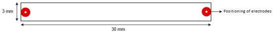
Figure 1.
Illustration of the test structure, the wires are connected at the indicated points.
Two layers of ink were printed on each sample using a PIXDRO LP50 (Meyer Burger Technology AG, Thun, Netherlands) system with a Spectra SE-128 AA 128 (Fujifilm Dimatix Inc., Santa Clara, CA, USA) 30 pL print head at a resolution of 600 × 600 dpi. Before printing the second layer the first had to sufficiently dry to obtain a homogenous surface and avoid spreading of ink (which depends on the cohesive forces of the ink and the adhesive forces between the ink and the substrate) [56,57]. To promote the evaporation of solvents and hence accelerate the drying process, the substrate table was heated to 57 °C. Subsequently, the samples were sintered in order to achieve formation of a compact, homogeneous layer. For the type 4 and p_e:smart® paper substrates, photonic curing (PulseForge 1200, Novacentrix, Austin, TX, USA) with an overall sintering energy of 2.1 J/cm2 and 1 J/cm2 was employed, respectively. The used photonic curing parameters were obtained by iteratively approaching optimum values. The other samples were sintered thermally in an oven. The employed sintering parameters are summarized in Table 1.

Table 1.
Overview of the used sintering parameters for the Ag nanoparticle ink on different substrates.
The electrical properties of the samples were determined using an LCR meter (measurement device for measuring inductance L, capacitance C, resistance R) (1V DC, Wayne Kerr (Iserlohn, Germany) Precision Analyzer 6440B) and statistically analyzed before and after contacting the samples with enamelled copper wires (Ø 120 µm). In this way the influence of the junctions on the electrical properties, such as the conductivity, could be determined.
For the contacting, four different possibilities have been investigated: (a) direct soldering on the inkjet-printed structures using standard solder (Sn62Pb36Ag2, 2.5% 1.1.2.B flux, Stannol, Velbert, Germany) at a temperature of 265 °C, (b) screen printing Ag pads (Novacentrix HPS-FG32 Ag screen ink) and subsequent soldering using commercial standard solder (Sn62Pb36Ag2, 2.5% 1.1.2.B flux, Stannol) at 265 °C, (c) adhesive bonding with a commercially available conductive polyurethane glue (Polytec PT (Karlsbad, Germany) PU 1000) then cured at 60 °C for 1 h in an oven and (d) mechanical connection using customary crimps for flexible printed electronics (Memcon (Kiel, Germany) Short Male Contacts).
For the damp-heat the samples were exposed to 85% relative humidity at 85 °C for 140 h inside of a climate chamber. Again, the junctions’ conductivities were measured before and after the damp-heat test.
To determine the mechanical stability of the individual joints, destructive tensile testing using a digital pressure and tensile force measurement device (Sauter (Metzingen, Germany) FK50) with peak-hold-function was conducted. The measurement device was designed for measuring forces up to 50 N at a resolution of 0.02 N. For the tensile testing, the sample was fastened to the rigidly attached measurement device, as illustrated in Figure 2. The sample was pulled downwards vertically with continuously increasing force until the connection broke. The maximum applied force before the connection failed was recorded by the device’s peak-hold function. One sample set was tested right after contacting while the second set consisted of the samples that were exposed to the damp-heat test before.
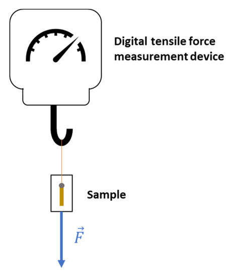
Figure 2.
Schematic illustration of the measurement setup for the tensile test.
3. Results
3.1. Sample Characterization before Connecting
The resistance values of the printed test structures show moderate reproducibility, as listed in Table 2. On rather porous substrates, such as the type 4 paper substrate and the p_e:smart® capacity paper, the ink is expected to be partially absorbed. According to the literature, this leads on one hand to an improved adhesion, while on the other hand the reproducibility might be reduced [58]. Consequently, the resistance on type 4 shows an empirical standard deviation of 18% from the mean value. However, the lowest reproducibility (empirical standard deviation of 20% of the mean value) was achieved on Kemafoil® PET.
Table 2.
Overview on the measured resistance values of the test structures on different substrates before connecting (9 samples each). Meaning of abbreviations: Avg.—average, Std.Dev.—standard deviation.
3.2. Sample Characterization after Connecting
As described in Section 2, all samples were connected to copper wires using (a) direct soldering, (b) soldering on screen printed Agpads, (c) adhesive bonding and (d) crimping. The resistance values of the copper wires were in the range of a few mΩ.
The direct soldering at 265 °C processing temperature was applicable for the connection of type 4 paper, p_e:smart®, Mylar® PET and Kemafoil®, yet with some restrictions. On Mylar® PET and Kemafoil®, some of the samples were only poorly contacted, or experienced ablation of the printed layers during soldering or the subsequent handling, as illustrated in Figure 3a. Similarly, on Kapton® the Ag layer ablated directly during soldering and therefore no electrical contact could be established. In contrast to that, the soldering on the screen-printed pads worked for all structures on all substrates under test, and the connections appeared to be mechanically stable during ordinary handling and showed good conductivity. Nevertheless, on some samples the printed layers were damaged due to the high temperatures during soldering, as illustrated for p_e:smart® in Figure 3c.
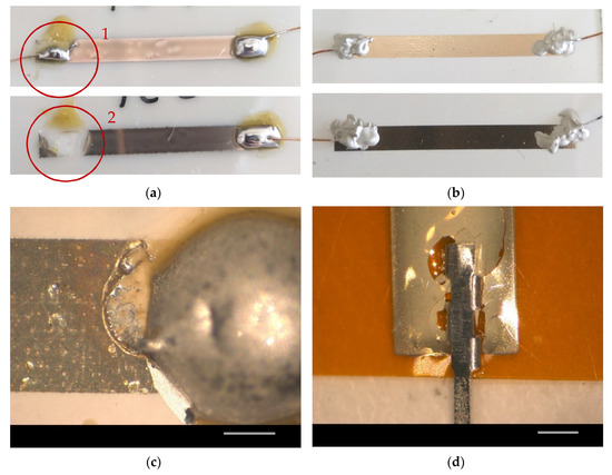
Figure 3.
(a) Direct soldering on Mylar® PET in some cases leads to poor contacting (1) or even ablation of the printed structures (2); (b) Contacting using adhesive bonding on two different samples on p_e:smart® paper; (c) Soldering on Ag pads on p_e:smart®—poor contacting due to damage of the printed layer; the scale bar corresponds to 1 mm; (d) Contacting using crimping on Kapton®, the printed layer is destroyed during processing; the scale bar corresponds to 1 mm.
The adhesive bonding using conductive glue was also applicable for all substrates under test; however, the total resistance more than doubled. Furthermore, this method showed low stability as even minor movements at the junctions lead to non-negligible changes in the measurement signals. Figure 3b shows a contacted p_e:smart® paper substrate sample using adhesive bonding. However, for the applicability in 2.5D electronics, the vertical expansion (thickness) of the contact points has to be considered as well. This is where adhesive bonding with an average height of 0.58 mm performed best, as listed in Table 3. The purely mechanical contacting using crimps resulted in low mechanical stability, high contact resistances or even contact errors for most of the samples. On Kapton® the printed layer even ablated due to the applied mechanical forces during crimping (as illustrated in Figure 3d). This method only worked for some samples on the white PET substrate, yet the crimping process itself was difficult to handle and hardly reproducible. Besides that, the crimping resulted in comparatively thick and rigid connection points, which is not desired in 2.5D printed and flexible electronics applications (see Table 3). Therefore, crimping was excluded from any further observations.
Table 3.
Overview of the thickness of the different connection methods.
As expected, the overall resistance increased for all connection methods. The adhesive bonding resulted in the highest increase in the samples’ total resistance values (around 50%), followed by soldering on Ag pads. The results of the overall applicability are summarized in Table 4.
Table 4.
Assessment of the suitability of different connection techniques on different substrates 1.
3.3. Sample Characterization after Damp-Heat Testing
In a first step the influence of the damp-heat test (140 h stored at 85 °C/85 % rH) on the conductivity of the printed layers was studied without considering the connections. The test induced some significant re-sintering and post-curing effects on the polymer-based substrates. On Mylar® PET the average resistance even halved. In contrast to that, on both paper substrates the median and mean values stayed in the same range, while the scattering increased and hence the reproducibility decreased. A statistical representation of the resistance values of the samples under test before and after exposure to damp-heat is illustrated in Figure 4.
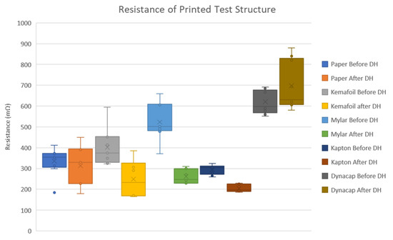
Figure 4.
Boxplot of the resistance values of the printed test structures before and after damp heat (DH) testing.
In the second step, the influence of the damp-heat test on the electrical properties of the individual connections was investigated. To this end, the percentage changes in the total resistance of the individual samples due to the connections before and after the test were evaluated. All in all, the adhesive bonding performed best, as all glued joints remained electrically conductive after the test. However, for some samples the conductivity dramatically decreased, e.g., on type 4 paper substrate the increase in resistance was up to 150% (see Figure 5a). The soldering on Ag pads showed superior electrical performance on Mylar® PET and p_e:smart®, with deviations in the range of less than 20% and less than 30% before and after the exposure to damp-heat, respectively (see Figure 5b,d). In contrast to that, not a single soldered connection on Ag pads on type 4 paper substrate showed any electrical conductivity after the test (Figure 5a). For the other substrates, this solution can be considered as mediocre from a purely electrical point of view (e.g., see Figure 5c). The direct soldering remained electrically stable on p_e:smart® paper, and the relative deviation of the sample’s resistance due to the connection even decreased, as illustrated in Figure 5d. Except for one sample, the direct soldering also showed decent results on the type 4 paper substrates (Figure 5a). For the polymer-based substrates, this connection strategy appears to be inappropriate, as hardly any connection could be established.
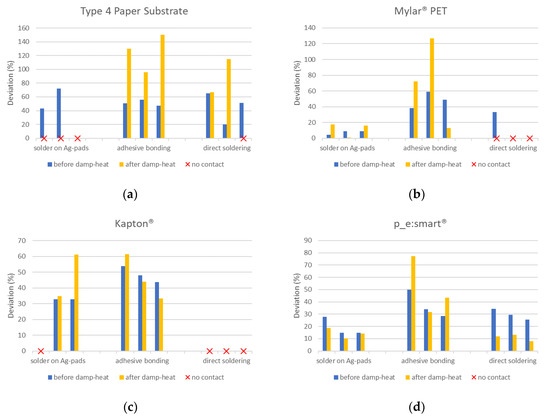
Figure 5.
Deviations of the samples’ total resistances due to the different contacting methods before and after damp-heat testing (85 °C/85%) on (a) type 4 paper substrate, (b) Mylar® PET, (c) Kapton® and (d) p_e:smart®.
Table 5 summarises the applicability of the different connection strategies on all used substrates after the damp-heat testing.
Table 5.
Assessment of the suitability of different connection techniques on different substrates after damp-heat testing (85 °C/85% rH) 1. Abbreviation: excl.—excluded.
3.4. Tensile Testing
For the destructive tensile testing, the mechanical durabilities of two sample sets were studied. The first set consisted of contacted samples before damp-heat testing, while the second set consisted of contacted samples after damp-heat testing. The occurring failure types were classified into three different categories: (a) ablation of the connection; (b) tearing of the copper wire; and (c) detachment of the copper wire. Generally, most connections appear to be mechanically quite stable, before as well as after the damp-heat test. The soldering on Ag pads resulted in excellent results for the Mylar® PET, as illustrated in Figure 6b. The connections of both sample sets withstood tensile forces between 9 N and 12 N. For the first sample set, not a single connection broke, but in all cases the copper wire tore. However, the mechanical stability appeared to be slightly reduced, due to the damp-heat testing, as for the second sample set ablation occurred in two out of six cases. The worst performance in the case of soldering on Ag pads was observed on Kapton®. Most connections ablated already during handling, while the remaining ones withstood only comparatively low forces. The corresponding failure type for all samples was ablation.
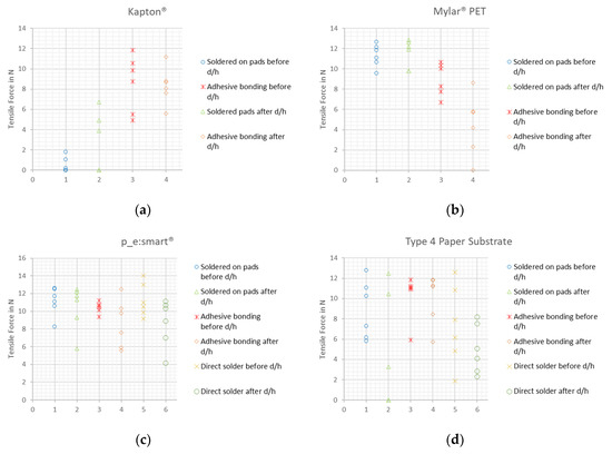
Figure 6.
Overview of the maximum tensile forces of the different connection strategies before and after damp-heat testing on (a) Kapton®, (b) Mylar® PET, (c) p_e:smart®, and (d) type 4 paper substrate.
Figure 7a shows a p_e:smart® sample with connections soldered on Ag pads after tensile testing where the copper wire tore due to the mechanical load, while the connection itself remained intact. Figure 7b shows an ablated connection on type 4 paper substrate.
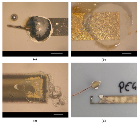
Figure 7.
(a) Connections soldered on Ag pads on a p_e:smart® sample after tensile testing without damp-heat; the copper wire tore under the applied tensile force, the scale bar corresponds to 2 mm; (b) Ablated connection soldered on Ag pads on a type 4 paper substrate after tensile testing without damp-heat, the scale bar corresponds to 1 mm; (c) Ablated adhesive bonding on Mylar® PET substrate before damp-heat and after tensile testing, the scale bar corresponds to 1 mm; (d) Ablated adhesive bonding on Mylar® PET substrate after damp-heat and tensile testing.
The adhesive bonding also led to decent mechanical stability on most substrates, except for Mylar® PET. The most common type of failure was the pulling of the copper wire out of the joint. Although the mechanical stability on Kapton was not superior, adhesive bonding has proven to be the most stable connection strategy for Kapton® (see Figure 6a). A contrary behavior can be observed on Mylar® PET, as illustrated in Figure 6b. The first sample set showed moderate stability, wherein pulling the wire out of the joint was the most common failure type, but ablation also occurred. After damp-heat testing, the mechanical stability on Mylar® PET was drastically reduced. All connections ablated together with the printed layers, as illustrated in Figure 7d. Direct soldering was only possible on the two paper substrates. On p_e:smart®, the connections were mechanically stable even though some degradation became observable after damp-heat testing (see Figure 6c). On the type 4 paper substrate, similar results were obtained (see Figure 6d).
4. Discussion
Direct soldering led to comparatively poor results on the polymer-based substrates, i.e., a conductive connection could only be established on the paper substrates (type 4 paper and p_e:smart®), yet with some restrictions. The advantage of direct soldering is that no curing is required, and the connection can be established within one single processing step. However, inkjet-printed layers have a comparatively low thickness, in the range of a few micrometres, therefore the heat is basically directly transferred to the substrate leading to ablation of the printed layer. This might be attributed to the different thermal expansion coefficients between electrode and substrate. Upon rapid heating, the material expansions are different, resulting in stress that leads to delamination. Although a connection could be established for some samples, the direct soldering requires advanced soldering skills as the substrate should not be touched with the soldering iron for too long. Usually, in hand-soldering, temperatures above 350 °C and contact durations of a few seconds are desired to facilitate the evaporation and decomposition of the corrosive ingredients of the fluxing agent [59], which cannot be done when working with sensitive specimens. Furthermore, it is not feasible to clean the residual soldering flux off without damaging the printed structure, hence no cleaning was done. The fluxing agent of the used solder contains halogen, which is known to promote corrosion [59,60]. After the damp-heat test, dissolving of the printed layer could be observed in many cases; furthermore, the adhesion decreased. The associated visually observable discoloration of the residual flux indicates that chemical and structural changes have indeed taken place. The practicability and performance of flux-free soldering has to be investigated, as part of future works.
In contrast to that, the soldering on screen-printed Ag pads has proven to be comparatively stable on most substrates except for the uncoated type 4 paper substrate. This behavior was expected, as successful soldering on screen printed structures has been reported in the literature [36]. The ablation of the soldered screen-printed contacts on the type 4 paper substrate after damp-heat testing might be explained by the poor adhesion of the screen-printed layer on the inkjet-printed layer, while a vast majority of the inkjet-printed pattern remains attached to the paper substrate, as illustrated in Figure 7b. This can be due to fiber swelling effects [61], where the uncoated fibrous substrate absorbs a lot of humidity, leading to an expansion of individual fibres. Again, this condition can lead to the alteration of the ink-substrate interplay and a drastic reduction in the adhesion to the substrate. Furthermore, at the edges of the screen-printed pads the corrosive nature of the soldering flux combined with high temperatures can lead to destruction of the inkjet-printed Ag layer (see Figure 7b). On the other hand, considering the damp-heat as well as the tensile testing on p_e:smart® and Mylar® PET, the best connection could be achieved with soldering on Ag pads. Here, the contact resistances were low, while providing superior mechanical durability.
Purely mechanical contacting using customary crimps for printed electronics applications led to the worst results on all substrates under test. As the crimp connections are established under application of comparatively high mechanical forces, the printed layers tend to be damaged during processing. Furthermore, the crimps resulted in rigid and relatively thick connections, which is unfavourable for flexible 2.5D electronics applications. The handling of the crimps turned out to be quite difficult from a usability point of view, yet special tools might simplify the use of this contacting method.
The highest versatility and overall stability could be achieved by employing adhesive bonding. Although the connections using conductive glue resulted in the greatest contact resistances, the connections remained stable after damp-heat testing and showed superior adhesion on all but one substrate under test. This exception is Mylar® PET, where the mechanical stability was only mediocre from the beginning, and the adhesion dramatically decreased after the damp-heat testing as the subsequent tensile test revealed. The optical microscopy images indicate that before damp-heat testing, the printed layer remained adherent to the substrate (see Figure 7c), while after the damp-heat test the contact ablated together with the printed Ag layer (see Figure 7d). From a usability point of view, it is quite challenging to apply adhesive bonding without using specialized expensive tools. As a result, the joints differ in size and form, reducing the overall reproducibility of the process (see Figure 3b). Additionally, to improve adhesion, the electrodes should be cleaned before applying the conductive glue. For printed electrodes this is not possible, as cleaning agents might damage the printed layers. On the paper-based substrates, cleaning liquids would be absorbed and consequently lead to fiber swelling. As cleaning is obviously not trivial in this case, careful handling of the samples and a clean working routine is required to avoid contamination in advance. Another point to consider is the adhesive bonding’s low electrical stability during movement. Even minor displacements of the wires resulted in non-negligible distortions of the measurement results, which needs to be taken into account when the flexibility and wearability of hybrid electronics are in demand.
The electrical characterization of the inkjet-printed samples revealed that for the polymer-based substrates post-curing or re-sintering effects during damp-heat testing occurred. As those samples were initially sintered at much higher temperatures than 85 °C, the decrease in resistance must rather be attributed to the storage at high humidity or to a certain combination of both conditions. Similarly, such a humidity sintering effect has been observed by Andersson et al. [62], who exploited this effect for the development of a resistive humidity sensor with memory effect. In a further study, they observed that this behavior can most likely be attributed to certain ions in the substrate’s coating [63]. The presence of silver halides on the nanoparticles’ surfaces might reduce the conductivity while increasing the required sintering energy of the printed layer. Chloride and bromide ions can precipitate silver ions, resulting in an overall decrease in the resistance, as also reported by Tang et al. [64]. However, in the present paper the used polymer-based substrates were all uncoated. Even Mylar® PET, on which this effect was most pronounced, was untreated. The climate chamber is operated with demineralized water; therefore, it is unlikely that this effect might be attributed to the presence of ions in the environment. Hence, the observed low temperature–high humidity sintering effect needs to be studied more thoroughly as part of future works. For the paper-based substrates, the median and mean resistance values remained stable, yet the scattering of the values increased. This can be attributed to the fiber swelling effect [61]. As fibrous paper substrates consist of purely statistically oriented fibers, this effect varies to different degrees for the individual samples, resulting in a broader distribution of the resistance values [65].
5. Conclusions
The electrical characteristics, durability and mechanical stability of four different commonly applied connection strategies with five commercially available substrates for the hybrid integration of inkjet-printed electronics were investigated. The present work demonstrates that although some connection strategies generally appear to be more appealing than others, the used substrate and the individual target application, as well as the associated requirements, need to be considered carefully when choosing a connection technology. Nevertheless, considering the current state of the art, adhesive bonding appears to be the most appropriate and is highly versatile for the hybrid integration of inkjet-printed electronics. On the other hand, mechanical contacting, namely crimping, can easily damage the printed structure, leading to the worst results of all methods evaluated.
Author Contributions
Conceptualization, L.R. and J.Z.; methodology, L.R..; formal analysis, L.R., J.Z., T.S.; data curation, L.R. and J.Z.; writing—original draft preparation, L.R., J.Z., T.S., H.Z. and L.-M.F.; writing—review and editing, L.R., J.Z., T.S., H.Z. and L.-M.F.; supervision, H.Z. and L.-M.F.; project administration, L.R. All authors have read and agreed to the published version of the manuscript.
Funding
This work has been conducted as part of the research project Smarter Leichtbau 4.0 funded by the European Regional Development Fund (ERDF).
Conflicts of Interest
The authors declare no conflict of interest.
References
- Beedasy, V.; Smith, P.J. Printed electronics as prepared by inkjet printing. Materials 2020, 13, 704. [Google Scholar] [CrossRef] [PubMed]
- Chang, J.S.; Facchetti, A.F.; Reuss, R. A circuits and systems perspective of organic/printed electronics: Review, challenges, and contemporary and emerging design approaches. Eee J. Emerg. Sel. Top. Circuits Syst. 2017, 7, 7–26. [Google Scholar] [CrossRef]
- Mohammed, M.G.; Kramer, R. All-printed flexible and stretchable electronics. Adv. Mater. 2017, 29. [Google Scholar] [CrossRef]
- Nag, A.; Mukhopadhyay, S.C.; Kosel, J. Wearable flexible sensors: A review. IEEE Sens. J. 2017, 17, 3949–3960. [Google Scholar] [CrossRef]
- Liu, J.; Liu, M.; Bai, Y.; Zhang, J.; Liu, H.; Zhu, W. Recent progress in flexiblewearable sensors for vital sign monitoring. Sensors 2020, 20, 4009. [Google Scholar] [CrossRef] [PubMed]
- Sekine, T.; Sugano, R.; Tashiro, T.; Sato, J.; Takeda, Y.; Matsui, H.; Kumaki, D.; Santos, F.D.D.; Miyabo, A.; Tokito, S. Fully printed wearable vital sensor for human pulse rate monitoring using ferroelectric polymer. Sci. Rep. 2018, 8, 4442. [Google Scholar] [CrossRef] [PubMed]
- Khan, S.; Ali, S.; Bermak, A. Recent developments in printing flexible and wearable sensing electronics for healthcare applications. Sensors 2019, 19, 1230. [Google Scholar] [CrossRef]
- Ali, S.; Khan, S.; Bermak, A. All-printed human activity monitoring and energy harvesting device for internet of thing applications. Sensors 2019, 19, 1197. [Google Scholar] [CrossRef]
- Agarwala, S.; Yeong, W.Y. Aerosol jet fabricated biodegradable antenna for bioelectronics application. In Proceedings of the Additive Manufacturing Meets Medicine, Lübeck, Germany, 12–13 September 2019. [Google Scholar]
- Khaleel, H.R. Design and fabrication of compact inkjet printed antennas for integration within flexible and wearable electronics. IEEE Trans. Compon. Packag. Manuf. Technol. 2014, 4, 1722–1728. [Google Scholar] [CrossRef]
- Guo, L.G.; Jiaheng, M.; Kwee, L.F.C.; Agarwala, S.; Wai, Y.Y.; Zhang, Y.P. Inkjet-printed patch antenna emitter for wireless communication application. Virtual Phys. Prototyp. 2016, 11, 289–294. [Google Scholar]
- Krivec, M.; Stockinger, T.; Zikulnig, J.; Eibensteiner, F.; Müller, U. Printed 2D proton sensor for in-situ measurement in glue lines. Proceedings 2018, 2, 990. [Google Scholar] [CrossRef]
- Yang, Y.; Chiesura, G.; Vervust, T.; Bossuyt, F.; Luyckx, G.; Degriek, J.; Vanfleteren, J. Design and fabrication of a flexible dielectric sensor system for in situ and real-time production monitoring of glass fibre reinforced composites. Sens. Actuators A: Phys. 2016, 243, 103–110. [Google Scholar] [CrossRef]
- Zymelka, D.; Togashi, K.; Kobayashi, T. Concentric array of printed strain sensors for structural health monitoring. Sensors 2020, 20, 1997. [Google Scholar] [CrossRef]
- Zhang, Y.; Anderson, N.; Bland, S.; Nutt, S.; Jursich, G.; Joshi, S. All-printed strain sensors: Building blocks of the aircraft structural health monitoring system. Sens. Actuators A: Phys. 2017, 253, 165–172. [Google Scholar] [CrossRef]
- Rausch, J.; Salun, L.; Griesheimer, S.; Ibis, M.; Werthschützky, R. Printed resistive strain sensors for monitoring of light-weight structures. In Proceedings of the Smart Sensor Phenomena, Technology, Networks, and Systems, San Diego, CA, USA, 15 April 2011; Volume 7982. [Google Scholar]
- Sowade, E.; Ramon, E.; Mitra, K.Y.; Martínez-Domingo, C.; Pedró, M.; Pallarès, J.; Loffredo, F.; Villani, F.; Gomes, H.L.; Terés, L.; et al. All-inkjet-printed thin-film transistors: Manufacturing process reliability by root cause analysis. Sci. Rep. 2016, 6, 33490. [Google Scholar] [CrossRef]
- Gu, Y.; Park, D.; Gonya, S.; Jendrisak, J.; Das, S.; Hines, D.R. Direct-write printed broadband inductors. Addit. Manuf. 2019, 30. [Google Scholar] [CrossRef]
- Correia, V.; Mitra, K.Y.; Rocha, J.G.; Sowade, E.; Baumann, R.R.; Lanceros-Mendez, S. Design and fabrication of multilayer inkjet-printed passive components for printed electronics circuit development. J. Manuf. Process. 2017, 31, 364–371. [Google Scholar] [CrossRef]
- Huber, B.A.; Popp, P.; Kaiser, M.; Ruediger, A.; Schindler, C. Fully inkjet printed flexible resistive memory. Appl. Phys. Lett. 2017. [CrossRef]
- Pang, Y.; Cao, Y.; Chu, Y.; Liu, M.; Snyder, K.; MacKenzie, D.; Cao, C. Additive manufacturing of batteries. Adv. Funct. Mater. 2019, 30. [Google Scholar] [CrossRef]
- Subramanian, V.; Chang, J.B.; Vornbrock, A.d.; Huang, D.C.; Jagannathan, L.; Liao, F.; Mattis, B.; Molesa, S.; Redinger, D.R.; Soltman, D.; et al. Printed electronics for low-cost electronic systems: Technology status and application development. In Proceedings of the ESSCIRC 2008—34th European Solid-State Circuits Conference, Edinburgh, UK, 15–19 September 2008. [Google Scholar]
- Khan, Y.; Thielens, A.; Muin, S.; Ting, J.; Baumbauer, C.; Arias, A.C. A new frontier of printed electronics: Flexible hybrid electronics. Adv. Mater. 2019. [CrossRef]
- Serpelloni, M.; Cantù, E.; Borghetti, M.; Sardini, E. Printed smart devices on cellulose-based materials by means of aerosol-jet printing and photonic curing. Sensors 2020, 20, 841. [Google Scholar] [CrossRef] [PubMed]
- Muhaisin, M.M.; Khan, R.A.; Telfort, J.; Heger, W.; Roberts, G.W. Opportunities and challenges in desktop-inkjet based flexible hybrid electronics. In Proceedings of the 2019 IEEE 62nd International Midwest Symposium on Circuits and Systems (MWSCAS), Dallas, TX, USA, 4–7 August 2019. [Google Scholar]
- Nilsson, H.-E.; Unander, T.; Sidén, J.; Andersson, H.; Manuilskiy, A.; Hummelgård, M.; Gulliksson, M. System Integration of Electronic Functions in Smart Packaging Applications. IEEE Trans. Compon. Packag. Manuf. Technol. 2012, 2, 1723–1734. [Google Scholar] [CrossRef]
- Roscher, F.; Thalheim, R.; Seifert, T.; Paul, S.-D.; Zichner, R.; Wiemer, M.; Otto, T. Joining two worlds—Hybrid integration of silicon based electronics and printed functionalities. In Proceedings of the Smart Systems Integration; 13th International Conference and Exhibition on Integration Issues of Miniaturized Systems, Barcelona, Spain, 10–11 April 2019. [Google Scholar]
- Kim, C.; Espalin, D.; Liang, M.; Xin, H.; Cuaron, A.; Varela, I.; Macdonald, E.; Wicker, R.B. 3D printed electronics with high performance. Multi-Layer. Electr. Interconnect IEEE Access 2017, 5, 25286–25294. [Google Scholar]
- Faller, L.-M.; Zikulnig, J.; Krivec, M.; Roshanghias, A.; Abram, A.; Zangl, H. Hybrid printing for the fabrication of smart sensors. J. Vis. Exp. 2019. [CrossRef]
- Faller, L.-M.; Lenzhofer, M.; Hirschl, C.; Kraft, M.; Zangl, H. Characterization of a robust 3D- and inkjet-printed capacitive position sensor for a spectrometer application. Sensors 2019, 19, 443. [Google Scholar] [CrossRef]
- Goh, G.L.; Agarwala, S.; Goh, G.D.; Tan, H.K.J.; Zhao, L.; Chuah, T.K.; Yeong, W.Y. Additively manufactured multi-material free-form structure with printed electronics. Int. J. Adv. Manuf. Technol. 2017, 94, 1309–1316. [Google Scholar] [CrossRef]
- DeGraff, J.; Liang, R.; Le, M.Q.; Capsal, J.-F.; Ganet, F.; Cottinet, P.-J. Printable low-cost and flexible carbon nanotube buckypaper. Mater. Des. 2017, 133, 47–53. [Google Scholar] [CrossRef]
- Rajala, S.; Tuukkanen, S.; Halttunen, J. Characteristics of piezoelectric polymer film sensors with solution-processable graphene-based electrode materials. IEEE Sens. J. 2015, 15. [Google Scholar] [CrossRef]
- Baptist, J.R.; Zhang, R.; Wei, D.; Saadatzi, M.N.; Popa, D.O. Fabrication of strain gauge based sensors for tactile skins. In Proceedings of the Smart Biomedical and Physiological Sensor Technology XIV, Anaheim, CA, USA, 22 May 2017; Volume 10216. [Google Scholar]
- Dimitrov, M.; Pelz, P.F.; Lyashenko, A.; Tehrani, A.H.; Dörsam, E. Measurement system by printed thin pressure sensor array. In Proceedings of the 9th International Fluid Power Conference, Aachen, Germany, 24–26 March 2014; Volume 3. [Google Scholar]
- Li, X.; Andersson, H.; Sidén, J.; Schön, T. Soldering surface mount components on screen printed Ag patterns on paper and Polyimide substrates for hybrid printed electronics. Flex. Print. Electron. 2018, 3. [Google Scholar] [CrossRef]
- Li, Z.; Zhang, R.; Moon, K.; Liu, Y.; Hansen, K.; Le, T.; Wong, C.P. Highly conductive, flexible, polyurethane-based adhesives for flexible and printed electronics. Adv. Funct. Mater. 2012. [Google Scholar] [CrossRef]
- Wu, H.; Cheng, Y.; Liu, J.; Cui, X.; Xie, B.; Zhang, Z. A highly conductive thermoplastic electrically conductive adhesive for flexible and low cost electronics. In Proceedings of the 15th International Conference on Electronic Packaging Technology, Chengdu, China, 12–15 August 2014. [Google Scholar]
- Siegel, A.C.; Phillips, S.T.; Dickey, M.D.; Lu, N.; Suo, Z.; Whitesides, G.M. Foldable printed circuit boards on paper substrates. Adv. Funct. Mater. 2010. [Google Scholar] [CrossRef]
- Andersson, H.; Andres, B.; Manuilskiy, A.; Forsberg, S.; Hummelgard, M.; Bäckström, J.; Zhang, R.; Olin, H. Contacting paper-based supercapacitors to printed electronics on paper substrates. Nord. Pulp Pap. Res. J. 2018, 27, 476–480. [Google Scholar] [CrossRef]
- Perelaer, J.; Schubert, U.S. Inkjet printing of interconnects and contacts based on inorganic nanoparticles for printed electronics applications. In Inkjet-Based Micromanufacturing; WILEY-VCH Verlag GmbH & Co. KGaA: Weinheim, Germany, 2012; pp. 347–364. [Google Scholar]
- Gordon, R. Electrically Conductive Adhesives 2016–2026; IDTechEx: London, UK, 1 April 2016; Available online: https://www.idtechex.com/research/reports/electrically-conductive-adhesives-2016-2026-000469.asp (accessed on 28 May 2018).
- Mattana, G.; Briand, D. Recent advances in printed sensors on foil. Mater. Today 2016, 19, 88–99. [Google Scholar] [CrossRef]
- Dankoco, M.D.; Tesfay, G.Y.; Benevent, E.; Bendahan, M. Temperature sensor realized by inkjet printing process on flexible substrate. Mater. Sci. Eng. B 2015. [Google Scholar] [CrossRef]
- Zikulnig, J.; Hirschl, C.; Rauter, L.; Krivec, M.; Lammer, H.; Riemelmoser, F.; Roshanghias, A. Inkjet printing and characterisation of a resistive temperature sensor on paper substrate. Flex. Print. Electron. 2019, 4. [Google Scholar] [CrossRef]
- Sung, K.-H.; Park, J.; Kang, H. Multi-layer inkjet printing of Ag nanoparticle inks andits sintering with a near-infrared system. Int. J. Precis. Eng. Manuf. 2018, 19, 303–307. [Google Scholar] [CrossRef]
- Huttunen, O.-H.; Happonen, T.; Hiitola-Keinänen, J.; Korhonen, P.; Ollila, J.; Hiltunen, J. Roll-To-Roll screen-printed silver conductors on a polydimethyl siloxane substrate for stretchable electronics. Ind. Eng. Chem. Res. 2019, 58, 19909–19916. [Google Scholar] [CrossRef]
- Rasul, J.S. Chip on paper technology utilizing anisotropically conductive adhesive for smart label applications. Microelectron. Reliab. 2004, 44, 135–140. [Google Scholar] [CrossRef]
- Andersson, H.A.; Manuilskiy, A.; Haller, S.; Hummelgard, M.; Sidén, J.; Hummelgard, C.; Olin, H.; Nilsson, H.-E. Assembling surface mounted components on ink-jet printed double sided paper circuit board. Nanotechnology 2014, 25. [Google Scholar] [CrossRef]
- Li, X.; Sidén, J.; Andersson, H.; Sawatdee, A.; Öhman, R.; Eriksson, J.; Genchel, T. Enabling paper-based flexible circuits with aluminium and copper conductors. Flex. Print. Electron. 2019, 4. [Google Scholar] [CrossRef]
- Zhu, J.; Koehl, M.; Hoffmann, S.; Berger, K.A.; Zamini, S.; Bennett, I.; Gerritsen, E.; Malbranche, P.; Pugliatti, P.; di Stefano, A.; et al. Changes of solar cell parameters during damp-heat exposure. Prog. Photovolt. 2016, 24, 1346–1358. [Google Scholar] [CrossRef]
- Faye, I.; Ndiaye, A.; Gecke, R.; Blieske, U.; Kobor, D.; Camara, M. Experimental study of observed defects in mini-modules based on crystalline silicone solar cell under damp heat and thermal cycle testing. Sol. Energy 2019, 191, 161–166. [Google Scholar] [CrossRef]
- Jagt, J.C. Reliability of electrically conductive adhesive joints for surface mount applications: A summary of the state of the art. IEEE Trans. Compon. Packag. Manuf. Technol. Part A 1998, 21, 215–225. [Google Scholar] [CrossRef]
- Ivanov, V.; Boehme, B.; Wolter, K.-J. Resistance of conductive adhesive joints on non-noble surface finishes. In Proceedings of the 35th International Spring Seminar on Electronics Technology, Bad Aussee, Austria, 9–13 May 2012. [Google Scholar]
- Neff, C.; Eston, E.; Schrand, A. Interconnections for additively manufactured hybridized printed electronics in harsh environments. Designs 2020, 4, 14. [Google Scholar] [CrossRef]
- Lee, S.H.; Cho, Y.J. Characterization of silver inkjet overlap-printing through cohesion and adhesion. J. Electr. Eng. Technol. 2012, 7, 91–96. [Google Scholar] [CrossRef]
- Lee, S.H.; Shin, K.Y.; Hwang, J.Y.; Kang, K.T.; Kang, H.S. Silver inkjet printing with control of surface energy and substrate temperature. J. Micromech. Microeng. 2008, 18. [Google Scholar] [CrossRef]
- Öhlund, T.; Örtegren, J.; Forsberg, S.; Nilsson, H.-E. Paper surfaces for metal nanoparticle inkjet printing. Appl. Surf. Sci. 2012, 259, 731–739. [Google Scholar] [CrossRef]
- Jellesen, M.S.; Verdingovas, V.; Conseil, H.; Piotrowska, K.; Ambat, R. Corrosion in electronics: Overview of failures and countermeasures. In Proceedings of the European Corrosion Congress, Pisa, Italy, 11 September 2014. [Google Scholar]
- Puechagut, C.; Laügt, A.-M.; Guéné, E.; Anisko, R. Solder paste residue corrosivity assessment: Bono test. In Proceedings of the 2015 European Microelectronics Packaging Conference (EMPC), Friedrichshafen, Germany, 14–16 September 2015; pp. 1–7. [Google Scholar]
- Bollström, R.; Pettersson, F.; Dolietis, P.; Preston, J.; Österbacka, R.; Toivakka, M. Impact of humidity on functionality of on-paper printed electronics. Nanotechnology 2014, 25. [Google Scholar] [CrossRef]
- Andersson, H.; Manuilskiy, A.; Unander, T.; Lidenmark, C.; Forberg, S.; Nilsson, H.-E. Inkjet printed silver nanoparticle humidity sensor with memory effect on paper. IEEE Sens. J. 2012, 12, 1901–1905. [Google Scholar] [CrossRef]
- Andersson, H.; Manuilskiy, A.; Lindenmark, C.; Gao, J.; Öhlund, T.; Forsberg, S.; Örtegren, J.; Schmidt, W.; Nilsson, H.-E. The influence of paper coating content onroom temperature sintering of silvernanoparticle ink. Nanotechnology 2013, 24, 455203. [Google Scholar] [CrossRef]
- Tang, Y.; He, W.; Zhou, G.; Wang, S.; Yang, X.; Tao, Z.; Zhou, J. A new approach causing the patterns fabricated by silver nanoparticles to be conductive without sintering. Nanotechnology 2012, 23, 355304. [Google Scholar] [CrossRef] [PubMed]
- Zikulnig, J.; Roshanghias, A.; Rauter, L.; Hirschl, C. Evaluation of the sheet resistance of inkjet-printed ag-layers on flexible, uncoated paper substrates using van-der-pauw’s method. Sensors 2020, 20, 2398. [Google Scholar] [CrossRef] [PubMed]
© 2020 by the authors. Licensee MDPI, Basel, Switzerland. This article is an open access article distributed under the terms and conditions of the Creative Commons Attribution (CC BY) license (http://creativecommons.org/licenses/by/4.0/).