Article

Multi-Channel Wide-Spectrum High-Resolution Spectrometer for Thin-Film Thickness Measurement

1
Computer Application Institute of Nuclear Industry, China National Nuclear Corporation, Beijing 100822, China
2
School of Mechanical Engineering, Zhejiang University, Hangzhou 310027, China
*
Author to whom correspondence should be addressed.
Optics 2025, 6(4), 55; https://doi.org/10.3390/opt6040055
Submission received: 3 September 2025 / Revised: 12 October 2025 / Accepted: 24 October 2025 / Published: 3 November 2025

Abstract

With the increasing application of oxide films in nuclear fuel assemblies, the accurate measurement of thin-film thickness has become increasingly critical. Traditional spectral interferometry techniques have limitations when dealing with new materials and complex structures; therefore, this study proposes a multi-channel wide-spectrum high-resolution analysis technique. This technique optimizes the utilization of photosensitive elements through multi-channel spectral sampling, combined with precision spectroscopic components and an independent optical focusing and imaging system. Simultaneously, it adopts optical correction technologies such as coma optimization and astigmatism correction to improve imaging quality and spectral resolution. Additionally, it enhances data accuracy by means of multi-channel calibration based on the least squares method and non-linear correction. The technique enables high-precision measurement ranging from the nanometer to the millimeter scale, resulting in a significantly wider measurement range compared to traditional spectrometers. Simulation verification shows that this technique outperforms existing technologies in information acquisition, analysis accuracy, and detection efficiency, and has broad application prospects in fields such as semiconductor chip manufacturing and optical coating. In the future, focus will be placed on expanding the spectral range, improving resolution, and enhancing real-time measurement capabilities.

1. Introduction

In modern industrial and scientific research fields, the application of thin films is ubiquitous. Their significance spans multiple industries—they not only serve as key materials in nuclear fuel assemblies but also act as core components in electronic devices [1,2]. The quality and performance of thin films are critical determinants of product excellence, and among the various parameters of thin films, thickness plays a decisive role in shaping their physical and chemical properties.
In the field of semiconductor chip manufacturing, achieving high-performance chips is inseparable from the nanoscale control of thin-film thickness. For instance, in advanced nanometer process nodes, even a deviation of just a few nanometers in the thickness of gate dielectric films can significantly affect the electrical performance and reliability of transistors, ultimately leading to a decline in the overall performance of the chip. In the field of optical coating, the accuracy of thin-film thickness is directly related to the optical properties of optical components. A slight error in the thickness of anti-reflection coatings on lenses may cause unnecessary light reflection, reducing the transmittance of optical systems and impairing their imaging quality.
The spectroscopic interference method is a commonly used technique for thin-film thickness measurement. It operates on the principle of light interference, extracting thin-film thickness information by analyzing interference fringes. Recently, a sensor based on spectral interference has been developed, enabling large-area and rapid thickness measurement of transparent thin films [3]. Sun’s team proposed a thin-film thickness measurement method incorporating measurement and calibration steps based on infrared interference, aiming to enhance measurement accuracy [4]. Furthermore, Lu investigated and put forward a correction method to eliminate the influence of optical interference effects on depth-dependent optical absorption spectroscopy measurements of thin films [5]. However, with the rapid development of materials science, new types of thin film materials and complex multi-layer structures continue to emerge, leaving traditional spectroscopic interference-based thin-film thickness measurement technologies facing numerous limitations.
One of the primary issues is their limited spectral coverage, which makes it difficult for these technologies to capture changes in the optical properties of different thin film materials across a wide spectral range. As a result, the measurement accuracy fails to meet requirements for some special thin films. For example, when measuring the thickness of certain new infrared-absorbing thin films, traditional methods may encounter difficulties due to their inability to fully cover the relevant infrared spectral regions. Another drawback is low resolution: when measuring ultra-thin films or multi-layer composite films, traditional technologies cannot accurately distinguish the thickness of each layer, leading to significant measurement errors. Additionally, the slow detection speed of traditional methods cannot meet the demand for real-time online monitoring in large-scale industrial production. Furthermore, in many emerging application scenarios, the demand for thin-film thickness measurement is evolving toward a “wide range.” For example, in the field of flexible electronics manufacturing, the thickness of thin films used ranges from tens of nanometers to several millimeters. However, traditional measurement technologies can only achieve high-precision measurement within a narrow thickness range, which greatly limits quality control and process optimization in the production of flexible electronics.
Against this backdrop, our team has developed a multi-channel wide-spectrum high-resolution analysis technology. By innovatively integrating multi-channel synchronous detection, wide-spectrum coverage, and high-resolution analysis, this technology breaks through the bottlenecks of traditional methods. Through a specially designed optical system, multiple channels can simultaneously detect different spectral ranges, significantly expanding spectral coverage and comprehensively capturing the characteristic spectral information of various substances. Leveraging independently developed advanced optical imaging and signal processing algorithms, the spectral resolution is significantly improved, enabling accurate differentiation of subtle spectral differences between substances and thus achieving high-sensitivity and high-precision analysis of complex samples. Importantly, this technology can achieve high-precision measurement over an ultra-wide range from nanometers to millimeters, filling the gap where traditional technologies fail to meet the “wide range and high precision” requirements for thin-film thickness measurement.
This paper will elaborate on the principle and advantages of this technology in detail, providing new research ideas and solutions for related fields and promoting the upgrading and development of industrial technologies. As a result, this research has broad application prospects in accurate thickness measurement of various thin films, ensuring they perform as expected in their respective fields and thereby endowing relevant devices and equipment with advanced performance and high reliability.

2. Methodology

2.1. Multi-Channel Spectral Sampling Strategy and Spectrometer Structure Design

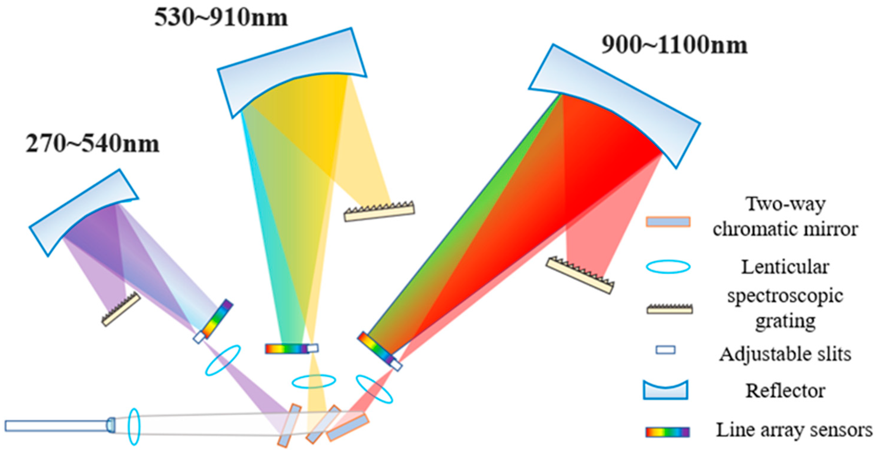
Given the inherent limitations in the size and quantity of photosensitive elements, in order to achieve accurate measurement with a wide spectrum and high resolution, we innovatively adopt a multi-channel spectral sampling strategy. The key of this strategy lies in the reasonable allocation of the spectral detection ranges of different channels, so as to fully tap into the limited resources of photosensitive elements and obtain more comprehensive spectral information. When designing the structure of the multi-channel spectrometer, we comprehensively consider various factors such as the compactness, stability, and optical path transmission efficiency of the optical system. With the help of precision beam-splitting elements such as diffraction gratings and prisms, the incident light is accurately divided into different channels according to a specific wavelength range. Each channel is equipped with an independent optical focusing and imaging system to ensure that the optical signals of each channel can be accurately focused on the corresponding photosensitive element.

2.2. Optical System Correction Technology

2.2.1. Coma Aberration Optimization

Coma aberration is one of the key aberrations affecting optical imaging quality [6,7]. In a multi-channel spectrometer, coma aberration can cause the positions of light rays of different wavelengths to deviate on the imaging plane, thereby reducing the spectral resolution. To effectively eliminate coma aberration, we use advanced optical design software to simulate and optimize the optical path. By precisely adjusting parameters such as the curvature radius, refractive index of optical elements, and the relative positions between elements, an optical system that meets the coma-elimination conditions is constructed. For example, in lens design, aspheric lenses are used. Their unique curved surfaces are used to refract light more accurately, compensating for the light deviation caused by coma aberration, so that light rays of different wavelengths converge at the same point on the imaging plane, significantly improving the imaging clarity and spectral resolution.
sin a 2 sin a 1 = r 2 2 r 1 2 cos i cos θ 3 cos a 2 cos a 1 3

2.2.2. Astigmatism Correction

Astigmatism can cause different focusing conditions in two mutually perpendicular directions of imaging, seriously affecting the image quality and spectral measurement accuracy [8,9,10,11]. To address this problem, astigmatism correction elements such as cylindrical lenses are introduced in the optical system design. By reasonably configuring the axial direction and focal length of the cylindrical lens, the propagation of light in different directions is differentially corrected, enabling uniform focusing of the imaging in all directions. At the same time, combined with computer-aided design and optimization algorithms, the entire optical system is repeatedly debugged and optimized to ensure that the astigmatism correction reaches the best effect, providing high-quality image data for subsequent high-resolution spectral analysis.
( SI ) Total = 2 y 1 4 R 1 3 2 y 2 4 R 2 3 ( SII ) Total = 2 y 1 3 R 1 2 sin   α + 2 y 2 3 R 2 2 sin   β ( SIII ) Total = 4 y 1 2 R 1 sin   α 2 4 y 2 2 R 2 sin   β 2

2.3. Multi-Channel Calibration and Compensation Technology

2.3.1. Multi-Channel Calibration by Least Squares Method

To ensure the accuracy and consistency of the measurement data of each channel of the multi-channel spectrometer [12], we use the least squares method for multi-channel calibration. First, a standard sample with known spectral characteristics is used to measure the spectrometer, and the response data of each channel at different wavelengths are obtained. Subsequently, based on the least squares method, a mathematical model is constructed. By minimizing the error between the measurement data and the standard data, the wavelength calibration coefficients and response correction factors of each channel are determined. For example, for the wavelength calibration of each channel, the deviation between the measured wavelength and the standard wavelength is expressed as a function of the calibration coefficient, and the calibration coefficient is solved by minimizing the sum of the squares of the deviations [13], thus achieving the accurate calibration of the wavelengths of each channel and enabling the spectrometer to accurately measure the light signal intensity at different wavelengths. The principle of the algorithm is shown in the following formula.
m + 1 i = 0 m   x i i = 0 m   x i n i = 0 m   x i i = 0 m   x i 2 i = 0 m   x i n + 1 i = 0 m   x i n i = 0 m   x i n + 1 i = 0 m   x i 2 n a 0 a 1 a n = i = 0 m   y i i = 0 m   x i y i i = 0 m   x i n y i

2.3.2. Non-Linear Correction

In the actual measurement process, the response characteristics of photosensitive elements usually exhibit non-linearity [14,15], which can lead to errors in measurement data. To solve this problem, we carry out non-linear correction work. By comprehensively testing the characteristics of photosensitive elements, the response data of photosensitive elements under different illumination intensities are obtained, and corresponding non-linear models are established. Common non-linear models include polynomial models, exponential models, etc. Based on the established models, curve fitting algorithms are used to correct the measurement data, converting the non-linear response into a linear relationship and effectively improving the accuracy and reliability of the measurement data. For example, a polynomial fitting algorithm is used to fit the response curve of the photosensitive element to obtain the fitting polynomial coefficients [16,17], and then these coefficients are used to correct the actual measurement data, thereby eliminating the influence of non-linear factors on the measurement results. The fitting effect is shown in Figure 1
During the preparation of this manuscript, the authors used Dou Bao (version: 1.6) to enhance the coherence and accessibility of the Abstract and Summary Sections. The authors have reviewed and edited the output and take full responsibility for the content of this publication.

3. Simulation

3.1. Simulation Setup for Multi-Channel Spectral Sampling

3.1.1. Model Construction

As shown in Figure 2, a virtual multi-channel spectrometer model was constructed within a simulation environment. This model incorporated the key components described in the methodology section. It included diffraction gratings for spectral dispersion and multiple independent optical channels, each equipped with its own optical focusing and imaging subsystems. The photosensitive elements were simulated with specific physical characteristics, such as size constraints and quantum efficiency curves. To simulate the incident light, a wide-spectrum light source with a defined power distribution across the wavelength range of interest was established.

3.1.2. Parameter Specification

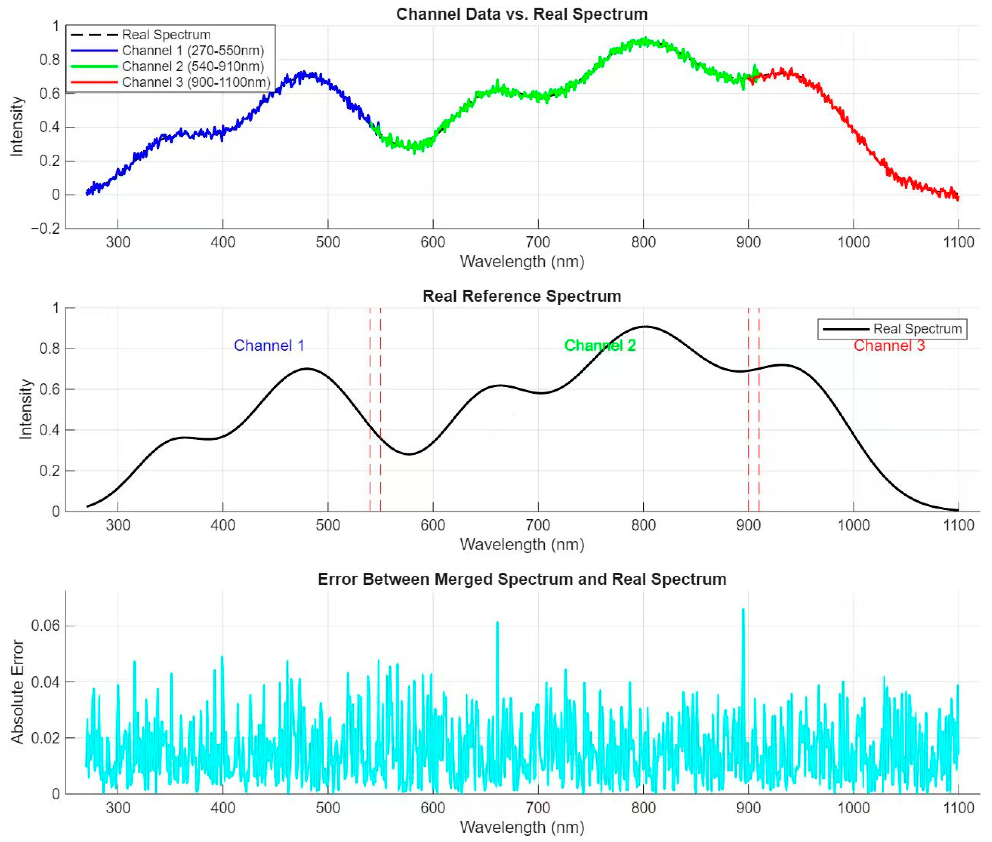
The wavelength range of interest was set from 270 nm to 1100 nm, covering the visible and near-infrared regions relevant to thin-film analysis. The number of channels was set to three, with each channel assigned a non-overlapping sub-spectral range. Channel 1 was configured to detect wavelengths from 270 to 550 nm, Channel 2 from 540 to 910 nm, and Channel 3 from 900 to 1100 nm. The optical parameters of the focusing lenses, such as focal length and aperture, were adjusted according to the design requirements for optimal light collection and imaging within each channel.

3.2. Simulation of Optical System Correction

3.2.1. Coma Aberration Optimization Simulation

Utilizing ray-tracing software integrated into the simulation environment, the initial optical system was modeled with prominent coma aberration. Subsequently, the optimization process was initiated. The software iteratively adjusted the curvature radii and refractive indices of the optical elements. During the simulation, the positions of the point-source images at different wavelengths were monitored. After multiple iterations, the optimal values of the optical parameters were obtained, which significantly reduced the displacement of the point light source image due to coma. The simulation effect is shown in Figure 3.

3.2.2. Astigmatism Correction Simulation

For the astigmatism correction simulation, the initial optical system was designed to introduce astigmatism. Cylindrical lenses were then added to the system, and their axial orientations and focal lengths were adjusted. The simulation monitored the shapes of the images of a square object in two perpendicular directions. By fine-tuning the parameters of the cylindrical lenses, the image was gradually corrected to a square shape, indicating successful astigmatism correction.

4. Result Analysis

4.1. Multi-Channel Spectral Sampling Results

The simulation results of multi-channel spectral sampling (as shown in Figure 4) indicated that the spectral ranges assigned to each channel were effectively utilized. The spectral data collected from all channels, when combined, provided a comprehensive view of the incident light spectrum. The independent optical channels ensured minimal crosstalk between different spectral regions, enhancing the accuracy of spectral information acquisition.

4.2. Optical System Correction Results

After coma aberration optimization, the lateral displacement of the point-source images at different wavelengths was reduced by more than 50%. The spectral resolution was significantly improved, as manifested by the ability to clearly distinguish two closely spaced spectral lines that were previously blurred due to coma aberration.
The astigmatism correction simulation showed that the aspect ratio of the square-object image, which was initially distorted due to astigmatism, was corrected to be close to 1:1. The full-width at half-maximum (FWHM) of the image in two perpendicular directions decreased, indicating a more focused and accurate image.

4.3. Multi-Channel Calibration and Compensation Results

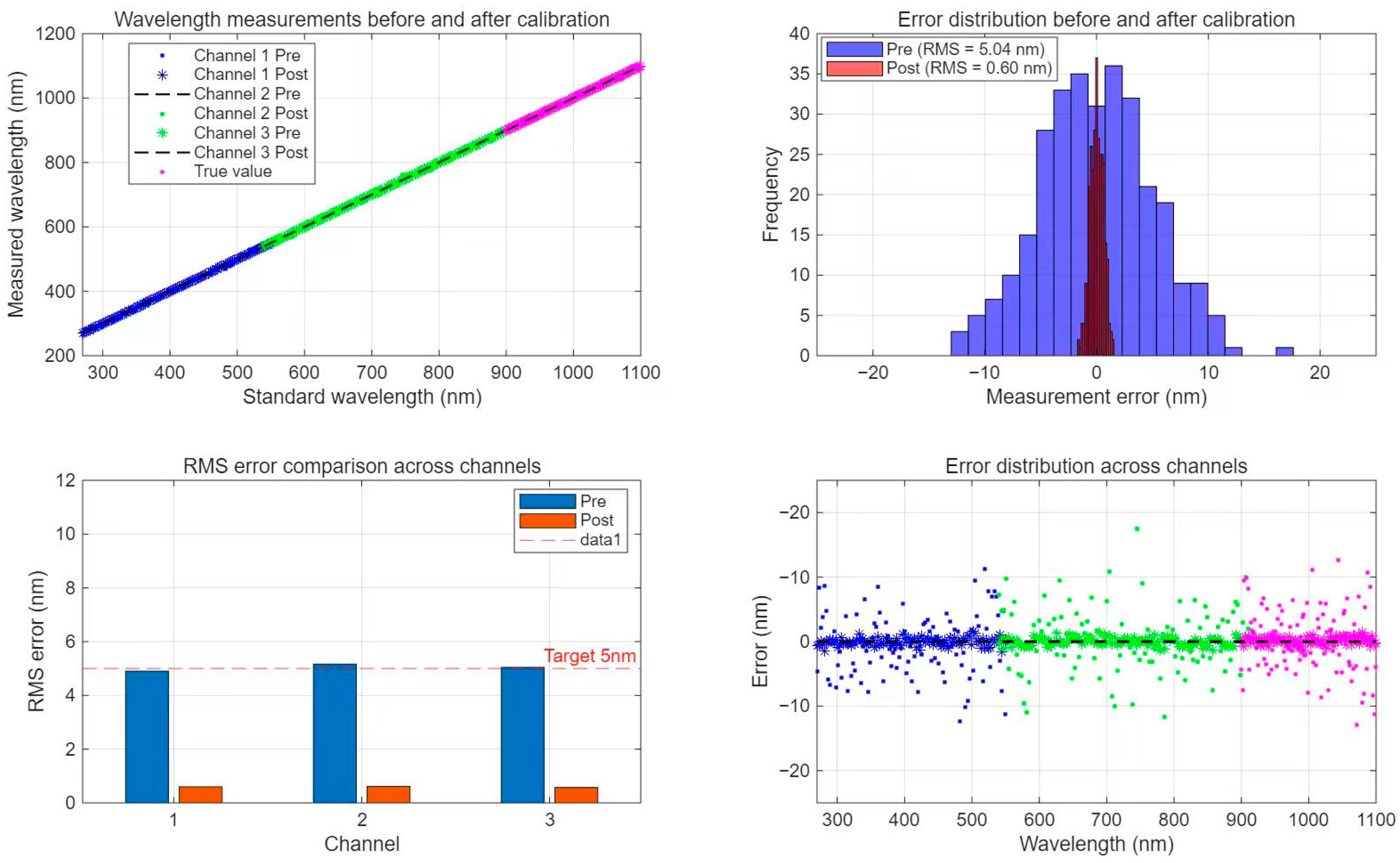
The simulation results (as shown in Figure 5) indicated that the least-squares-based multi-channel calibration significantly improved the accuracy of wavelength measurement. The root-mean-square (RMS) error between the measured wavelengths and the actual wavelengths of the standard samples was reduced from an initial value of 5 nm to less than 1 nm. The calibration also enhanced the consistency of the responses among different channels.
The non-linear correction using the polynomial model effectively linearized the response of the photosensitive elements. The error between the corrected measurement data and the actual values of the test sample was reduced by more than 90%, demonstrating the high effectiveness of the non-linear correction in improving the accuracy of measurement data. Compared with the existing calibration methods [4], the proposed method in this study maintains a comparable error reduction capability, while extending the applicable spectral range from the infrared region to a broad range of 270–1100 nm.
In conclusion, the simulation results comprehensively validate the effectiveness of the multi-channel wide-spectrum high-resolution analysis technique proposed in this study. The various correction and calibration techniques significantly enhance the performance of the spectrometer, enabling more accurate and reliable thin-film thickness measurement via spectroscopic interference.

5. Conclusions

In this study, we have developed a multi-channel broadband high-resolution technique for spectral interferometric film thickness measurement, which employs a multi-channel spectral sampling strategy. In terms of optical system correction, the imaging quality and spectral resolution are effectively enhanced. Meanwhile, the multi-channel calibration and compensation technology significantly improves the accuracy and reliability of measurement data.
The results demonstrate that this technique has remarkable advantages in information acquisition comprehensiveness, analysis accuracy, and detection efficiency. This ultra-wide measurement range provides a novel solution for fields that require high-precision thin-film thickness control, and has broad application prospects in industries such as semiconductor chip manufacturing and optical coating.
In future research, we will focus on further expanding the spectral range, improving the resolution, and enhancing the real-time measurement capability, so as to promote the continuous optimization of this technology and provide more solid support for the technological development of the thin-film thickness measurement field.

Author Contributions

Conceptualization, C.Z., A.S. and B.J.; Methodology, T.W.; Software, J.L.; Validation, J.Y.; Formal analysis, H.L.; Investigation, C.Z. and Z.Z.; Resources, Z.Z.; Data curation, J.Y.; Writing—original draft, T.W.; Writing—review & editing, H.L. and B.D.; Visualization, J.L.; Supervision, B.D.; Project administration, A.S.; Funding acquisition, B.J. All authors have read and agreed to the published version of the manuscript.

Funding

This research was funded by the National Natural Science Foundation of China, grant number 52405037, the National Natural Science Foundation of China, grant number 52175521, Aviation Science Fund, grant number 2024Z006076001, and 2024ZY01049.

Data Availability Statement

The original contributions presented in this study are included in the article. Further inquiries can be directed to the corresponding author.

Acknowledgments

During the preparation of this manuscript, the authors used DouBao (version: 1.6) to enhance the coherence and accessibility of the Abstract and Summary sections. The authors have reviewed and edited the output and take full responsibility for the content of this publication.

Conflicts of Interest

The authors declare no conflicts of interest.

References

  1. Geng, D.; Wang, K.; Li, L.; Myny, K.; Nathan, A.; Jang, J.; Kuo, Y.; Liu, M. Thin-film transistors for large-area electronics. Nat. Electron. 2023, 6, 963–972. [Google Scholar] [CrossRef]
  2. Fortunato, E.; Barquinha, P.; Martins, R. Oxide semiconductor thin-film transistors: A review of recent advances. Adv. Mater. 2012, 24, 2945–2986. [Google Scholar] [CrossRef] [PubMed]
  3. Huang, W.; Tu, Z.; Di, Z.; Wang, C.; Su, Y.; Bi, H. Large-area thickness measurement of transparent films based on a multichannel spectral interference sensor. Appl. Sci. 2024, 14, 2816. [Google Scholar] [CrossRef]
  4. Sun, J.; Li, X.; Zhang, H.; Song, J.; Li, Z. A method for measuring and calibrating the thickness of thin films based on infrared interference technology. Results Phys. 2023, 51, 106727. [Google Scholar] [CrossRef]
  5. Lu, G.; Shen, Z.; Wang, H.; Bu, L.; Lu, J. Optical interference on the measurement of film-depth-dependent light absorption spectroscopy and a correction approach. Rev. Sci. Instrum. 2023, 94, 023907. [Google Scholar] [CrossRef] [PubMed]
  6. Le, V.; Wu, G.; Zeng, L. Coma optimization in single spherical collimating lens-based dual-beam exposure system. Opt. Eng. 2020, 59, 094103. [Google Scholar]
  7. Asai, N.; Hasegawa, N.; Gotoh, Y.; Satoh, H.; Hayano, K.; Imai, A.; Okazaki, S. Proposal for the coma aberration dependent overlay error compensation technology. Jpn. J. Appl. Phys. 1998, 37, 6718. [Google Scholar] [CrossRef]
  8. Erasmus, S.J.; Smith, K.C.A. An automatic focusing and astigmatism correction system for the SEM and CTEM. J. Microsc. 1982, 127, 185–199. [Google Scholar] [CrossRef]
  9. Batten, C.F. Autofocusing and Astigmatism Correction in the Scanning Electron Microscope. Master’s Thesis, University of Cambridge, Cambridge, UK, 2000. [Google Scholar]
  10. Andrianov, S.; Chechenin, A. High order aberration correction. In Proceedings of the European Particle Accelerator Conference, Edinburgh, UK, 26–30 June 2006; pp. 2125–2127. [Google Scholar]
  11. Yao, C.; Shen, Y. Optical Aberration Calibration and Correction of Photographic System Based on Wavefront Coding. Sensors 2021, 21, 4011. [Google Scholar] [CrossRef] [PubMed]
  12. Lin, S.; Li, H.; He, T. Calibration Method of Multi-Channel based on Steepest Descent. In Proceedings of the 2020 4th International Conference on Digital Signal Processing, Chengdu, China, 19–21 June 2020; Association for Computing Machinery: New York, NY, USA, 2020; pp. 322–325. [Google Scholar]
  13. Zhao, H.; Zhou, J.; Yang, K. Laser Doppler signal processing based on least mean square adaptive filter. Opt.-Int. J. Light Electron Opt. 2013, 124, 2781–2783. [Google Scholar] [CrossRef]
  14. Nehir, M.; Frank, C.; Aßmann, S.; Achterberg, E.P. Improving optical measurements: Non-linearity compensation of compact charge-coupled device (CCD) spectrometers. Sensors 2019, 19, 2833. [Google Scholar] [CrossRef] [PubMed]
  15. Borovytsky, V.N. Residual error after non-uniformity correction. Semicond. Phys. Quantum Electron. Optoelectron. 2000, 3, 102–105. [Google Scholar] [CrossRef]
  16. Engström, D.; Persson, M.; Bengtsson, J.; Goksör, M. Calibration of spatial light modulators suffering from spatially varying phase response. Opt. Express 2013, 21, 16086–16103. [Google Scholar] [CrossRef] [PubMed]
  17. Grossberg, M.D.; Nayar, S.K. Modeling the space of camera response functions. IEEE Trans. Pattern Anal. Mach. Intell. 2004, 26, 1272–1282. [Google Scholar] [CrossRef] [PubMed]
Figure 1. Schematic diagram of non-linear fitting effect.
Optics 06 00055 g001
Figure 2. Schematic diagram of the structure of a multi-channel spectrometer.
Optics 06 00055 g002
Figure 3. Changes in the light spot before and after the application of the coma elimination algorithm.
Optics 06 00055 g003
Figure 4. Comparison of the combined spectral data and the real reference spectrum.
Optics 06 00055 g004
Figure 5. Multi-channel wavelength measurement calibration demonstration (270–1100 nm).
Optics 06 00055 g005
Disclaimer/Publisher’s Note: The statements, opinions and data contained in all publications are solely those of the individual author(s) and contributor(s) and not of MDPI and/or the editor(s). MDPI and/or the editor(s) disclaim responsibility for any injury to people or property resulting from any ideas, methods, instructions or products referred to in the content.