Abstract
The optical properties of a heterostructure containing GaSb/GaAs quantum dots (QDs) have been systematically investigated via photoluminescence (PL) measurements to gain insights into carrier dynamics. The QD and wetting layer (WL) emissions exhibit a complementary dependence on the excitation intensity and temperature, reflecting the interplay between carrier localization in the WL and carrier relaxation from the WL to the QDs. Carrier dynamics related to localization, injection, and recombination are further validated by time-resolved photoluminescence (TRPL). These findings highlight the necessity of carefully optimizing GaSb/GaAs QD structures to mitigate the impact of carrier localization, thereby enhancing the ultimate performance of devices utilizing these QDs as active region materials.
1. Introduction
Semiconductor quantum dots (QDs), characterized by three-dimensional quantum confinement that enables complete carrier localization and quantized energy states, have launched many new concepts and promising device applications since they were initially proposed in the 1980s [1,2,3,4]. A notable example is GaSb, which can be sandwiched between GaAs, Al(Ga)As, or InAlAs layers to form QDs with a staggered type-II band alignment [5,6,7,8]. The unique properties arising from this type-II band structure, such as long carrier lifetime and large valence-band offset, make the GaSb QDs highly attractive for special photonics device applications, including photovoltaic cells and infrared detectors [9,10,11,12]. The GaSb/GaAs QDs have been employed recently in the development of intermediate-band solar cells (IBSCs) with high conversion efficiencies [13,14,15], as their type-II band alignment offers advantages over conventional In(Ga)As/GaAs QDs for IBSC applications. More recently, GaSb QDs have also emerged as a promising indium-free candidate for achieving long coherence times in single-photon emitters and spin qubits operating within the telecom wavelength range [16].
Despite the exploitation of GaSb/GaAs QDs in various optoelectronic devices, their carrier dynamics remain complex [17,18]. Understanding these carrier dynamics is crucial for the development of next-generation photonic devices. This research therefore delves into carrier dynamics, with a particular focus on the impact of carrier localization on the photoluminescence (PL) of GaSb/GaAs QDs, to provide support for the advancement of optoelectronic devices based on these QD structures.
2. Materials and Methods
The GaSb/GaAs QD sample was grown on a semi-insulated GaAs (100) substrate by solid-source molecular beam epitaxy (MBE). It consisted of a single layer of GaSb QDs with a 100 nm GaAs capping layer on the top. The GaSb was deposited at a growth rate of 0.3 ML/s at 485 °C for a total coverage of 4 monolayers (MLs). The QD formation was confirmed by reflective high-energy electron diffraction (RHEED) during the growth. Additionally, one reference sample containing just the layer of GaSb QDs was grown under identical conditions without the GaAs capping layer for morphological study by atomic force microscope (AFM).
As shown in Figure 1a–c, the AFM reveals round-shaped QDs with a surface density of ~110 dots/µm2, an average height of (9.0 ± 1.5) nm, and an average diameter of (58.1 ± 6.1) nm. The density and dimensions are consistent with previously reported results for GaSb/GaAs QDs grown under similar conditions [6]. The cross-sectional Transmission Electron Microscopy (XTEM) images in Figure 1d,e show that the GaSb QDs shrink after the GaAs capping, reaching an average height of ~5 nm and an average diameter of ~30 nm. This size reduction is attributed to antimony–arsenic exchange on the dot surfaces during GaAs overgrowth. The XTEM also confirms the existence of a thin GaAsSb wetting layer (WL).
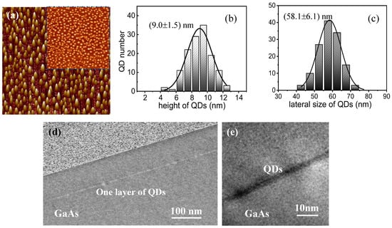
Figure 1.
(a) The 2 µm × 2 µm AFM image to show the GaSb QDs; (b,c) the height and diameter distribution of the QDs; (d,e) cross-section TEM images showing the GaSb QDs and WL.
The optical characteristics of QDs were investigated by PL and time-resolved photoluminescence (TRPL) measurements. For PL, the sample was mounted on the cold finger of a CCS-150 cryostat (Janis Research, Woburn, MA, USA) with the temperature controlled between 10 K and 300 K. A Mitutoyo NIR 50× objective lens (Mitutoyo, Kawasaki, Japan) focused a 532 nm continuous-wave (CW) laser beam onto the sample surface. Luminescence signal from the sample was collected by the same lens, dispersed by an Acton SpectraPro 2500i spectrometer (f = 50 cm, Teledyne Princeton Instruments Inc., Trenton, NJ, USA), and then detected by a PyLoN-IR InGaAs photodiode linear array (Teledyne Princeton Instruments Inc., Trenton, NJ, USA). For TRPL, excitation was provided by a MIRA 900 Ti–Sapphire mode-locked laser (780 nm, 78 MHz, ~2.7 ps pulse-width, Coherent Corp., Saxonburg, PA, USA), while the TRPL signal was measured by an infrared-enhanced C5680 streak camera system (Hamamatsu Photonics, Shizuoka, Japan) with a temporal resolution of ~35 ps.
3. Results and Discussion
Figure 2a shows the PL spectra measured at 10 K with a low excitation density of 0.03 W/cm2. Here, in addition to a luminescence peak at about 1.5 eV from the GaAs matrix, the sample shows two distinct peaks at 0.967 eV and 1.315 eV. The higher energy peak originates from the WL, while the lower energy peak is attributed to GaSb QD emission. The full width at half maximum (FWHM ~67.8 meV) and the peak position (0.967 eV) of the QD emission are similar to previously reported values for GaSb/GaAs QDs [19,20,21]. From the AFM data in Figure 1, the average distance between neighboring QDs is estimated to be ~40 nm, which is significantly smaller than the carrier diffusion length in GaAs [19,20]. Therefore, the observation of strong WL emission under a very low excitation intensity indicates that only a fraction of carriers diffuse and relax into the energy states of QDs, while most carriers localize and recombine within the WL. This occurs because the WL is generally imperfect, with interface and Sb/As composition modulations creating potential minima that trap carriers in localized states.
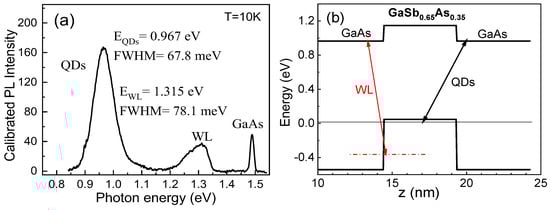
Figure 2.
(a) The PL spectrum was measured at 10 K with a low excitation intensity of 0.03 W/cm2; (b) the band structure calculated for the QDs (the arrows show the carrier recombination channels).
To gain a deeper insight into this QD system, we employed the nextnano software (version nextnano++) to simulate the band diagram using the measured QD dimensions from Figure 1e and the PL energies from Figure 2a. The simulation took a simple model that assumed pyramidal QDs and a homogeneous distribution of ternary GaAsSb. The calculated band diagram (Figure 2b) demonstrates the type-II band alignment and the indirect optical transitions between electrons and holes, while the holes are confined inside the GaSb region of the QDs (or the WL) and the electrons are in the surrounding GaAs barrier [21,22]. The band diagram also reveals a small conduction band (CB) offset of ~130 meV and a much larger valence-band confinement (~480 meV) for the holes in QDs.
Next, we measured the PL dependence on laser excitation intensity across the range of 0.03 W/cm2 to 30,000 W/cm2, shown in Figure 3a, while Figure 3b–d, respectively, provide the extracted peak energy shifts, the integrated PL intensities, and the percentage contributions of QD and WL peaks to the total integrated intensity. As expected for structures with a staggered type-II band alignment, both QD and WL peaks exhibit significant blue shifts with increasing excitation intensity. Figure 3b shows that the QD peak shift (ΔE = 105 meV) exceeds that of the WL (ΔE = 25 meV) by more than a factor of four over the entire excitation intensity range, while the GaAs peak shifts only 14 meV. The large blue shifts are attributed to a combination of state filling and band bending due to a dipole-layer formation between the positively charged holes inside the QDs (or WLs) and the negatively charged electrons in the surrounding GaAs barrier [23,24,25,26]. For QDs, we see that the blue shift intensifies above ~30 W/cm2, reinforcing the mechanisms of “band bending” and “Coulomb attraction” stemming from the type-II confinement of the electrons with respect to the holes [27,28].
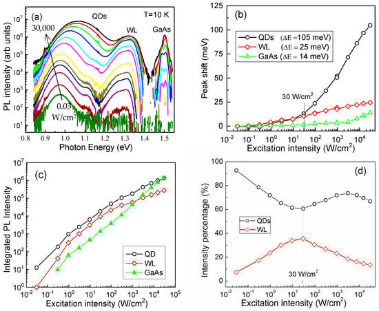
Figure 3.
(a) The evolution of PL spectra versus excitation intensity; (b) PL peak energy shift as a function of the excitation intensity for QDs, WL, and GaAs substrate peak; (c) the integrated PL intensity for the peaks of QDs, WL, and GaAs as a function of the excitation intensity; (d) the PL intensity weight for QDs and WL with respect to the excitation intensity.
The integrated PL intensity should scale proportionally with the population density of electrons and holes, i.e., the excitation density. Figure 3c confirms this monotonous increase for the QD, WL, and GaAs peaks, but with slightly different increase rates. To compare their relative changes, Figure 3d plots the percentage contribution of QD and WL emissions to the total intensity. It can be seen that the QD emission is much stronger than the WL at low excitation intensity. Then, with increasing excitation intensity, the WL contribution initially rises and then declines, while the QD contribution mirrors this trend. Their point of closest approach is around 30 W/cm2. This complimentary variation confirms that there are carriers localized within the WL and this effect strongly depends on the excitation intensity.
The correlated intensity variations for QD and WL peaks reflect the interplay between carrier localization within the WL and carrier injection from the WL to the QDs [29,30]. The 532 nm excitation laser has a penetration depth of ~300 nm, implying that the photo-generated carriers are primarily generated in the GaAs matrix. In general, most of these carriers are collected by the WL, and then relax into the lower energy states of GaSb QDs. However, Figure 3d shows that the WL emission gains intensity at the expense of the QD emission intensity for excitation below ~30 W/cm2. Thus, we conclude that some carriers become localized in the WL and the carrier localization strongly depends on the excitation intensity [17,31]. For excitation above ~30 W/cm2, the WL contribution decreases while the QD contribution increases. This reversal arises from a multiple-particle effect within the WL that enhances carrier scattering and promotes more carriers being transferred into QDs.
The temperature dependence of PL spectra was then measured under a fixed excitation intensity of 10 W/cm2, as shown in Figure 4a. We extracted the temperature dependence of the PL energies and integrated intensities for each peak in Figure 4b,c, respectively. Figure 4b reveals that the WL peak intensity decreases more rapidly than that of the QD peak, indicating accelerated carrier transfer from the WL to the QDs at elevated temperatures. Moreover, the WL peak vanishes at ~70 K, while the QD emission persists up to ~260 K. This suggests that carriers trapped by localized WL states become thermally activated, supplying additional carriers to the QD emission.
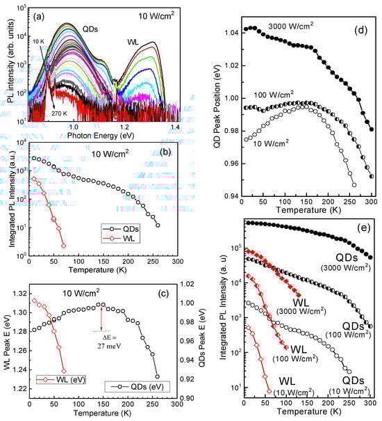
Figure 4.
(a) PL spectra versus temperature measured with the excitation intensity of 10 W/cm2; (b,c) show the integrated PL intensity and the peak energy for QD and WL peaks, respectively; (d,e) show the integrated PL intensity and the peak energy for the QD peak at three different excitation intensities.
We fit the PL integrated intensities in Figure 4b by using an Arrhenius equation:
where T is the temperature, I(T) is the PL integral intensity, E1 is the carrier local energy at low temperatures, and E2 is the carrier activation energy at high temperatures. E1 usually corresponds to the binding energy of the exciton, while E2 corresponds to the energy necessary for the exciton to escape from the bound energy state, then become captured by a non-radiative center [32]. The fitting results in activation energies for the WL of E1 = (6.5 ± 0.8) meV and E2 = (30.5 ± 3.2) meV, and of E1 = (9.2 ± 0.6) meV and E2 = (67.3 ± 14.0) meV for the QDs. In consideration of the band structure in Figure 2b, it is reasonable to associate E2 with the conduction band offset between GaAs and the WL or QDs.
Figure 4c plots the PL peak energies for both the QD and WL peaks as the temperature rises from 10 K to 260 K. It is very interesting that the QD emission peak shows an anomalous behavior, i.e., the QD PL peak blue shifts by ~27 meV when increasing the temperature from 10 K to 160 K. However, a QD emission peak should show a red shift due to the band gap shrinking with elevated temperature. We explain this anomalous blue shift by an increase in QD carrier density and the associated band bending. Due to carrier localization, the WL acts as a carrier reservoir. With increasing temperature, more localized carriers in the WL are activated by phonon interaction and then relax into the QDs. This provides more carriers for the QDs and increases the carrier density, resulting in the slow blue shift in the QD emission with elevated temperature. We should emphasize that such an anomalous blue shift would not happen if there were no carrier localization in the WL to supply additional carriers to the QDs.
To further investigate the localization of carriers in the WL and the interaction with QDs, we measured the PL with respect to temperature with increasing excitation intensities of 100 W/cm2 and 3000 W/cm2. The extracted peak energies for the QDs are shown in Figure 4d, while the integrated PL intensities for the QDs and the WL are shown in Figure 4e, respectively. We can see that the temperature dependence of the QD PL peak energy evolves significantly with increasing excitation intensity. At 100 W/cm2, it shows a successive red/blue/red shift (or decrease–increase–decrease; S-shaped behavior) with increasing temperature. Such an anomalous S-evolution, which has been well documented for many semiconductor QD structures, is generally attributed to the thermal activation and repopulation of trapped carriers due to carrier localization inside larger QDs [32,33,34]. Furthermore, at the highest excitation intensity of 3000 W/cm2, the QD peak energy exhibits a monotonous red shift as the temperature increases from 10 K to 300 K. Under this strong excitation, we speculate that multi-particle effects in the WL diminish the impact of carrier localization, thus leading to the more uniform filling of QD states.
Therefore, with increasing excitation from 10 W/cm2 to 100 W/cm2 and then to 3000 W/cm2, the dependence of QD PL peak energy on temperature transforms from an anomalous blue shift to an S-shaped behavior and finally to a monotonous red shift with elevated temperature. This transformation stems from the carrier localization in the WL and its dependence on the carrier density. This is further reflected by the integrated PL intensity variations in Figure 4e. Here, we see that the WL peak PL intensity decreases rapidly and vanishes by 60 K, 100 K, and 150 K for excitation with 10 W/cm2, 100 W/cm2, and 3000 W/cm2, respectively. Once WL emission is quenched within a specific temperature range, carrier localization within WL should no longer affect the dots, as no carriers remain in the WL to supply additional carriers to the dots. Due to carrier feeding from the WL, the QD emission intensity decays slowly until ~200 K for the excitation of 3000 W/cm2, followed by a relatively rapid quenching due to the activation of carriers from QDs to non-radiative centers.
Carrier dynamics were further investigated by TRPL experiments. First, we measured the PL spectrum to determine the QD and PL peaks using the Ti–Sapphire mode-locked laser (780 nm, 78 MHz, ~2.7 ps pulse-width) to provide excitation with an intensity of 3000 W/cm2, as shown in Figure 5a. Then, under the same excitation, we measured the decay curves for the QDs and the WL at the intensity maximum of each. As shown in Figure 5b, the QD decay curve exhibits a mono-exponential decay and it is fitted well by
where τ is the decay time constant, i.e., the carrier lifetime, and k is the decay amplitude constant. The extracted carrier lifetime for QDs is τ = (4.72 ± 0.73) ns, consistent with reported values (5~15 ns) for GaSb/GaAs QDs [22,35], but significantly longer than those (1~1.5 ns) of standard In(Ga)As/GaAs QDs [36]. In contrast, the WL emission demonstrates different dynamics. The observed decay for WL is non-linear and well-described by a bi-exponential decay function
where τ1 and τ2 are the decay time constants, and k1 and k2 are the decay amplitude constants. This results in τ1 = (0.28 ± 0.07) ns and τ2 = (1.78 ± 0.11) ns. The fast component is attributed to carrier injection from the WL to the QDs [6], while the slow component represents the radiative recombination of excitons of the WL. Here, both QDs and WL have long carrier lifetimes resulting from the type-II band alignment and spatial carrier separation [35,37].
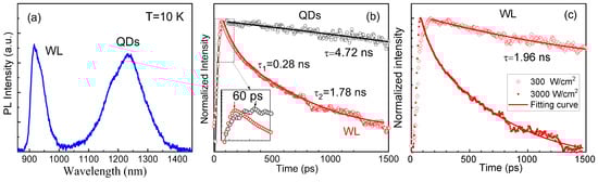
Figure 5.
(a) The PL spectrum measured with the pulse laser at 10 K; (b) decay curves for the QDs and the WL measured at the intensity maximum of each; (c) decay curves for WL emission at weak excitation (300 W/cm2) and strong excitation (3000 W/cm2), respectively.
Figure 5b also shows that the QD emission reaches its maximum intensity ~60 ps after the WL reaches its maximum. This delay may arise from different Coulomb interactions between positive and negative charges in the QDs and WL, or from the carrier injection process from the WL to the QDs. We suppose that under above-bandgap excitation, carriers are primarily generated in the GaAs matrix and then injected into the QDs through the WL, forming a complex system of coupled and time-dependent populations. The interplay between carrier localization in the WL and carrier injection from the WL into QDs, revealed in Figure 3, can cause the QD emission maximum to lag behind that of the WL emission [38].
Furthermore, both carrier localization within the WL and carrier rejection from the WL to the QDs depend on the excitation density. We therefore reduced the laser excitation by one order of magnitude to 300 W/cm2 to measure TRPL for WL. As shown in Figure 5c, the WL decay dramatically changes from the multi-exponential decay to a mono-exponential decay with a carrier lifetime of τ = (1.96 ± 0.09) ns. This change confirms that the recombination of carriers in the localized WL states takes a dominant role, while the carrier injection from the WL to QDs becomes negligible. Consequently, the QD emission was too weak to be measured reliably under this low excitation. It also should be mentioned that the carrier lifetime (τ = 1.96 ns) measured with the excitation of 300 W/cm2 is very close to the carrier lifetime of τ2 = 1.78 ns measured at the excitation of 3000 W/cm2. Both represent the radiative recombination of excitons within energy states of the WL. Furthermore, in Figure 5c, the WL emission reaches its maximum intensity ~90 ps earlier when excited at high power (3000 W/cm2) as opposed to lower power (300 W/cm2). This is the result of enhanced multi-particle effects from the strong excitation and higher carrier density in the WL.
The above PL and TRPL demonstrate that the carrier localization in the WL impedes carrier relaxation into the QDs. We attribute the primary cause of this carrier localization and the consequent slow carrier rejection to QDs to the spatial separation of the carriers confined in the WL and those confined in the QDs. As shown by the AFM and TEM data in Figure 1, the GaSb QDs have a surface density of ~110 dots/µm2 and an average diameter of ~30 nm; thus, the GaSb QDs are estimated to cover only ~7.8% of the WL surface. In this case, the carriers have a good possibility of being captured and trapped by the localized energy states of the WL where there are no QDs. This localization increases the carrier recombination inside the WL; thus, it may degrade the device performance for photovoltaic cells or photodetectors that use GaSb QDs for the active region. Therefore, this issue must be considered and the structures need to be carefully optimized to reduce the carrier localization impact and improve the ultimate device performance. In this scenario, in order to reduce the carrier localization in the WL, a possible solution is to increase the density of GaSb QDs to more completely cover the WL. For example, by increasing the GaSb growth rate or decreasing the substrate temperature, we would be able to increase the density of GaSb QDs by one order of magnitude to obtain ~1000 dots/µm2. It is reasonable to expect that the high density of GaSb QDs could enhance the carrier relaxation from the WL to the QDs, thus reducing the carrier localization in the WL.
4. Conclusions
In summary, the GaSb/GaAs QDs have been investigated by PL measurements. Both excitation-dependent and temperature-dependent luminescence behaviors are explained by carrier localization in the WL, reflecting the interplay of carrier localization in the WL with carrier relaxation from the WL to the dots. The carrier localization and related carrier dynamics are further verified by TRPL. The carrier localization in the WL can block carrier relaxation into the dots, while increasing recombination inside the WL. Due to the significance of carrier localization in the effective operation of optoelectronic devices based on GaSb QDs, the results of this research suggest that the GaSb QD structure should be carefully optimized to reduce the carrier localization impact in order to improve device performance.
Author Contributions
Conceptualization of QD structure, B.L.L. and Y.I.M.; methodology for optical measurements, S.-Y.M. and Y.W.; formal analysis, Y.W., M.E.W. and B.L.L.; investigation and validation, Y.W. and B.L.L.; resources, G.J.S.; writing—original draft preparation, Y.W., B.L.L. and M.E.W.; writing—review and editing, Y.I.M. and M.E.W.; supervision, G.J.S.; funding acquisition, Y.W. All authors have read and agreed to the published version of the manuscript.
Funding
Ying Wang acknowledges the support from the Natural Science Foundation of Hebei Province (F2025201068) and the Advanced Talents Incubation Program of the Hebei University (521100221052).
Data Availability Statement
The original contributions presented in this study are included in the article. Further inquiries can be directed to the corresponding author(s).
Conflicts of Interest
The authors declare no conflicts of interest.
Abbreviations
The following abbreviations are used in this manuscript:
| QD | Quantum dot |
| WL | Wetting layer |
| PL | Photoluminescence |
| TRPL | Time-resolved photoluminescence |
| MBE | Molecular beam epitaxy |
| RHEED | Reflective high-energy electron diffraction |
| AFM | Atomic force microscope |
| IBSC | Intermediate-band solar cells |
| XTEM | Cross-sectional Transmission Electron Microscopy |
| CW | Continuous-wave |
| CB | Conduction band |
References
- Michler, P. (Ed.) Single Quantum Dots: Fundamentals, Applications, and New Concepts; Topics in Applied Physics; Springer: Berlin/Heidelberg, Germany, 2003; Volume 90, pp. 1–86. ISSN 0303-4216. [Google Scholar]
- Bimberg, D.; Grundmann, M.; Ledentsov, N.N. Quantum Dot Heterostructures; Wiley: New York, NY, USA, 1998; pp. 1–19. [Google Scholar]
- Yuan, Z.; Kardynal, B.E.; Stevenson, R.M.; Shields, A.J.; Lobo, C.J.; Cooper, K.; Beattie, N.S.; Ritchie, D.A.; Pepper, M. Electrically driven single-photon source. Science 2002, 295, 102. [Google Scholar] [CrossRef] [PubMed]
- Bhattacharya, P.; Ghosh, S.; Stiff-Roberts, A.D. Quantum dot opto-electronic devices. Annu. Rev. Mater. Res. 2004, 34, 1–40. [Google Scholar] [CrossRef]
- Hatami, F.; Ledentsov, N.N.; Grundmann, M.; Böhrer, J.; Heinrichsdorff, F.; Beer, M.; Bimberg, D.; Ruvimov, S.S.; Werner, P.; Gosele, U.; et al. Radiative recombination in type-II GaSb/GaAs quantum dots. Appl. Phys. Lett. 1995, 67, 656. [Google Scholar] [CrossRef]
- Sun, C.-K.; Wang, G.; Bowers, J.E.; Brar, B.; Blank, H.-R.; Kroemer, H.; Pilkuhn, M.H. Optical investigations of the dynamic behavior of GaSb/GaAs quantum dots. Appl. Phys. Lett. 1996, 68, 1543. [Google Scholar] [CrossRef]
- Couto, D.D., Jr.; Almeida, P.T.d.; Santos, G.E.d.; Balanta, M.A.G.; Andriolo, H.F.; Brum, J.A.; Brasil, M.J.S.P.; Iikawa, F.; Liang, B.L.; Huffaker, D.L. Carrier dynamics dictated by bimolecular recombination in type-II quantum dots coupled to quantum wells. J. Appl. Phys. 2016, 120, 084305. [Google Scholar] [CrossRef]
- Yuan, Q.; Liang, B.L.; Luo, S.P.; Wang, Y.; Yan, Q.G.; Wang, S.F.; Fu, G.S.; Mazur, Y.I.; Maidaniuk, Y.; Ware, M.E.; et al. Type-II GaSb quantum dots grown on InAlAs/InP (001) by droplet epitaxy. Nanotechnology 2020, 31, 315701. [Google Scholar] [CrossRef]
- Geller, M.; Kapteyn, C.; Müller-Kirsch, L.; Heitz, R.; Bimberg, D. 450 meV hole localization in GaSb/GaAs quantum dots. Appl. Phys. Lett. 2003, 82, 2706. [Google Scholar] [CrossRef]
- Shoji, Y.; Tamaki, R.; Okada, Y. Temperature Dependence of Carrier Extraction Processes in GaSb/AlGaAs Quantum Nanostructure Intermediate-Band Solar Cells. Nanomaterials 2021, 11, 344. [Google Scholar] [CrossRef]
- Laghumavarapu, R.B.; Liang, B.L.; Bittner, Z.; Navruz, T.S.; Hubbard, S.; Huffaker, D.L. GaSb/InGaAs quantum dot-well hybrid structures as active regions in solar cells. Sol. Energy Mater. Sol. Cells 2013, 114, 165. [Google Scholar] [CrossRef]
- Lin, W.-H.; Tseng, C.-C.; Chao, K.-P.; Mai, S.-C.; Kung, S.-Y.; Wu, S.-Y. High-Temperature Operation GaSb/GaAs Quantum-Dot Infrared Photodetectors. IEEE Photonics Technol. Lett. 2011, 23, 106. [Google Scholar] [CrossRef]
- Ramiro, I.; Antolın, E.; Hwang, J.Y.; Teran, A.; Martin, A.J.; Linares, P.G.; Millunchick, J.; Phillips, J.; Marti, A.; Luque, A. Three-bandgap absolute quantum efficiency in GaSb/GaAs quantum dot intermediate band solar cells. IEEE J. Photovolt. JPV 2017, 7, 508. [Google Scholar] [CrossRef]
- Shoji, Y.; Tamaki, R.; Okada, Y. Multi-stacked GaSb/GaAs type-II quantum nanostructures for application to intermediate band solar cells. AIP Adv. 2017, 7, 065305. [Google Scholar] [CrossRef]
- Ramiro, I.; Villa, J.; Tablero, C.; Antolín, E.; Luque, A.; Martí, A.; Hwang, J.; Phillips, J.; Martin, A.J.; Millunchick, J. Analysis of the intermediate-band absorption properties of type-II GaSb/GaAs quantum-dot photovoltaics. Phys. Rev. B 2017, 96, 125422. [Google Scholar] [CrossRef]
- Michl, J.; Peniakov, G.; Pfenning, A.; Hilska, J.; Chellu, A.; Bader, A.; Guina, M.; Höfling, S.; Hakkarainen, T.; HuberLoyola, T. Strain-Free GaSb quantum dots as single-photon sources in the telecom S-band. Adv. Quantum Technol. 2023, 6, 2300180. [Google Scholar] [CrossRef]
- Baik, M.; Kyhm, J.H.; Kang, H.K.; Jeong, K.S.; Kim, J.S.; Cho, M.H.; Song, J.D. Optical characteristics of type-II hexagonal-shaped GaSb quantum dots on GaAs synthesized using nanowire self-growth mechanism from Ga metal droplet. Sci. Rep. 2021, 11, 7699. [Google Scholar] [CrossRef] [PubMed]
- Komolibus, K.; Piwonski, T.; Reyner, C.J.; Liang, B.L.; Huyet, G.; Huffaker, D.L.; Viktorov, E.A.; Houlihan, J. Absorption dynamics of type-II GaSb/GaAs quantum dots. Opt. Mater. Express 2017, 7, 1424. [Google Scholar] [CrossRef]
- Li, Z.-F.; Lu, W.; Liu, X.-Q.; Chen, X.-S.; Shen, S.C.; Fu, Y.; Willander, M.; Tan, H.H.; Jagdish, C. Determination of Carrier-Transfer Length from Side-Wall Quantum Well to Quantum Wire by Micro-Photoluminescence Scanning. J. Electron. Mater. 2003, 32, 913. [Google Scholar] [CrossRef]
- Niemeyer, M.; Ohlmann, J.; Walker, A.W.; Kleinschmidt, P.; Lang, R.; Hannappel, T.; Dimroth, F.; Lackner, D. Minority carrier diffusion length, lifetime and mobility in p-type GaAs and GaInAs. J. Appl. Phys. 2017, 122, 115702. [Google Scholar] [CrossRef]
- Kawazu, T.; Mano, T.; Noda, T.; Sakak, H. Optical properties of GaSb/GaAs type-II quantum dots grown by droplet epitaxy. Appl. Phys. Lett. 2009, 94, 081911. [Google Scholar] [CrossRef]
- Hatami, F.; Grundmann, M.; Ledentsov, N.N.; Heinrichsdorff, F.; Heitz, R.; Böhrer, J.; Bimberg, D.; Ruvimov, S.S.; Werner, P.; Ustinov, V.M.; et al. Carrier dynamics in type-II GaSb/GaAs quantum dots. Phys. Rev. B 1998, 57, 4635. [Google Scholar] [CrossRef]
- Alonso-Álvarez, D.; Alén, B.; García, J.M.; Ripalda, J.M. Optical investigation of type II GaSb/GaAs self-assembled quantum dots. Appl. Phys. Lett. 2007, 91, 263103. [Google Scholar] [CrossRef]
- Wang, Y.; Hu, S.H.; Xie, H.; Lin, H.Y.; Lu, H.B.; Wang, C.; Sun, Y.; Dai, N. Photoluminescence investigation of type-II GaSb/GaAs quantum dots grown by liquid phase epitaxy. Infrared Phys. Tech. 2018, 91, 68. [Google Scholar] [CrossRef]
- Gao, X.; Wei, Z.; Zhao, F.; Yang, Y.; Chen, R.; Fang, X.; Tang, J.; Fang, D.; Wang, D.; Li, R.; et al. Investigation of localized states in GaAsSb epilayers grown by molecular beam epitaxy. Sci. Rep. 2016, 6, 29112. [Google Scholar] [CrossRef] [PubMed]
- Motlan; Goldys, E.M. Photoluminescence of multilayer GaSb/GaAs self-assembled quantum dots grown by metalorganic chemical vapor deposition at atmospheric pressure. Appl. Phys. Lett. 2001, 79, 2976. [Google Scholar]
- Klenovský, P.; Steindl, P.; Geffroy, D. Excitonic structure and pumping power dependent emission blueshift of type-II quantum dots. Sci. Rep. 2017, 7, 45568. [Google Scholar] [CrossRef]
- Gradkowski, K.; Ochalski, T.J.; Williams, D.P.; Healy, S.B.; Tatebayashi, J.; Balakrishnan, G.; O’Reilly, E.P.; Huyet, G.; Huffaker, D.L. Coulomb effects in type-II Ga(As)Sb quantum dots. Phys. Stat. Sol. (b) 2009, 246, 752. [Google Scholar] [CrossRef]
- Zhou, X.L.; Chen, Y.H.; Jia, C.H.; Ye, X.L.; Xu, B.; Wang, Z.G. Interplay effects of temperature and injection power on photoluminescence of InAs/GaAs quantum dot with high and low areal density. J. Phys. D Appl. Phys. 2010, 43, 485102. [Google Scholar] [CrossRef]
- Liu, Y.; Wang, Y.; Liang, B.L.; Guo, Q.L.; Wang, S.F.; Fu, G.S.; Mazur, Y.I.; Ware, M.E.; Salamo, G.J. Interplay effect of excitation and temperature on carrier transfer between vertically aligned InAs/GaAs quantum dot pairs. Crystals 2016, 6, 144. [Google Scholar] [CrossRef]
- Hayne, M.; Maes, J.; Bersier, S.; Moshchalkov, V.V.; Schliwa, A.; Müller-Kirsch, L.; Kapteyn, C.; Heitz, R.; Bimberg, D. Electron localization by self-assembled GaSb/GaAs quantum dots. Appl. Phys. Lett. 2003, 82, 4355. [Google Scholar] [CrossRef]
- Li, H.; Wang, Y.; Guo, Y.N.; Wang, S.F.; Fu, G.S.; Mazur, Y.I.; Ware, M.E.; Salamo, G.J.; Liang, B.L. Complex exciton dynamics with elevated temperature in a GaAsSb/GaAs quantum well heterostructure. Appl. Phys. Lett. 2023, 122, 173105. [Google Scholar] [CrossRef]
- Lourenço, S.A.; Dias, I.F.L.; Duarte, J.L.; Laureto, E.; Aquino, V.M.; Harmand, J.C. Temperature-dependent photoluminescence spectra of GaAsSb/AlGaAs and GaAsSbN/GaAs single quantum wells under different excitation intensities. Braz. J. Phys. 2007, 37, 1212. [Google Scholar] [CrossRef]
- Dyksik, M.; Motyka, M.; Weih, R.; Hoefling, S.; Kamp, M.; Sek, G.; Misiewicz, J. Carrier transfer between confined and localized states in Type II InAs/GaAsSb quantum wells. Opt. Quantum Electron. 2017, 49, 59. [Google Scholar] [CrossRef]
- Liang, B.L.; Lin, A.; Pavarelli, N.; Reyner, C.J.; Tatebayashi, J.; Nunna, K.; He, J.; Ochalski, T.J.; Huyet, G.; Huffaker, D.L. GaSb/GaAs type-II quantum dots grown by droplet epitaxy. Nanotechnology 2009, 20, 455604. [Google Scholar] [CrossRef] [PubMed]
- Mazur, Y.I.; Wang, Z.M.; Tarasov, G.G.; Xiao, M.; Salamo, G.J.; Tomm, J.W.; Talalaev, V.; Kissel, H. Interdot carrier transfer in asymmetric bilayer InAs/GaAs quantum dot structures. Appl. Phys. Lett. 2005, 86, 063102. [Google Scholar] [CrossRef]
- Sun, M.; Simmonds, P.J.; Laghumavarapu, R.B.; Lin, A.; Reyner, C.J.; Duan, H.-S.; Liang, B.L.; Huffaker, D.L. Effects of GaAs(Sb) cladding layers on InAs/AlAsSb quantum dots. Appl. Phys. Lett. 2013, 102, 023107. [Google Scholar] [CrossRef]
- An, C.S.; Jang, Y.D.; Lee, H.; Lee, D.; Song, J.D.; Choi, W.J. Delayed emission from InGaAs/GaAs quantum dots grown by migration-enhanced epitaxy due to carrier localization in a wetting layer. J. Appl. Phys. 2013, 113, 173503. [Google Scholar] [CrossRef]
Disclaimer/Publisher’s Note: The statements, opinions and data contained in all publications are solely those of the individual author(s) and contributor(s) and not of MDPI and/or the editor(s). MDPI and/or the editor(s) disclaim responsibility for any injury to people or property resulting from any ideas, methods, instructions or products referred to in the content. |
© 2025 by the authors. Licensee MDPI, Basel, Switzerland. This article is an open access article distributed under the terms and conditions of the Creative Commons Attribution (CC BY) license (https://creativecommons.org/licenses/by/4.0/).