1. Introduction
The field of nanophotonics has been profoundly impacted by recent innovations in artificial intelligence (AI) paradigms, which have reshaped the landscape of design methodologies [
1,
2]. The process of designing complex photonic structures in the traditional forward approach, by using numerical methods, is usually computer-intensive. The core objective in nanophotonics is to manipulate light at subwavelength scales, thereby achieving desired behaviors in photonic structures. This manipulation involves finely tuning geometrical configurations to control sophisticated optical phenomena, such as plasmonic resonances and interferences. These phenomena are central to a wide range of applications, from achieving subwavelength focusing, which is essential for high-resolution imaging and sensing, to the development of advanced optical absorbers, applied in photovoltaic cells and optical filtering technologies [
3]. The ability to precisely tune the subwavelength geometries of these structures enables the manipulation of light in ways that were previously unattainable, opening new frontiers in optical technology.
The process of designing these subwavelength structures and predicting their behavior has been heavily dependent on numerical simulation, which requires the discretization and solution of local fields using Maxwell’s equations with finite element methods (FEMs) or the finite difference method (FDM), for example. These methods are powerful in that they allow for a detailed analysis of the electromagnetic behavior within photonic structures, accounting for factors such as material properties, geometric configuration, and local field interaction at the nanoscale.
However, the computational cost represents one of the primary challenges imposed by these traditional numerical methods [
1]. As the complexity of the structure increases, so does the number of elements that need to be solved in the simulation. Moreover, the size of the parametric search space—the range of variables over which the structure is optimized—can be overwhelming. This results in an exponential increase in computational requirements, making the design process not only time-consuming but also resource-intensive. This challenge is particularly pronounced when exploring a vast design space for the optimal configuration of a photonic structure, where thousands or even millions of potential configurations might need to be evaluated.
In response to these challenges, the integration of AI paradigms into nanophotonics has emerged as a revolutionary approach. AI, particularly deep learning techniques, offers an alternative pathway that can significantly reduce the computational costs of design in nanophotonics [
2,
4,
5]. These AI methods can learn from existing data and make predictions or suggest designs, thereby accelerating the design process. For instance, by training AI models on data generated from previous simulations, it is possible to predict the optical behavior of new photonic structures without the need for extensive numerical simulations. This not only speeds up the design process but also opens up new possibilities for exploring more complex and innovative photonic structures. Consequently, AI’s role in nanophotonics represents a paradigm shift, moving from traditional computation-intensive methods to more efficient, data-driven inverse design approaches.
The conceptualization of photonic devices through AI-aided inverse design has become a topic of interest in recent research. This approach has the potential to drastically reduce the time required for evaluating and designing complex subwavelength structures, a promise that has been documented in various prior studies. In [
6,
7], the authors used a neural network (NN) to approximate the light scattering of multilayer nanoparticles. The results showed that NN is a powerful tool for accelerating simulations about interactions with nanoscale structures. In another field of research, several papers have presented solutions for inverse design using deep learning (DL). As shown in [
8,
9,
10], the results demonstrated the efficiency of approaches based on NN in achieving the inverse design of multilayer nanoparticles and multilayer nanofilms, mid-infrared graphene plasmons, and plasmonic nanoantenna. As can also be seen in [
11,
12], inverse design, facilitated by AI, marks a significant departure from traditional methods, offering a more efficient pathway to achieving optimized photonic structures.
In the current work, we build upon these advancements and present a novel methodology for the design of a plasmonic absorber with applications in optical filtering. Central to our approach is the use of a trained artificial neural network (ANN) as a surrogate model. In conjunction with this, we employ a genetic algorithm (GA), an optimization technique inspired by the principles of natural selection, as our strategic search methodology. This algorithm systematically explores the parametric space to identify configurations that align with predefined performance goals, effectively narrowing down the most promising design options.
In this work, we propose a methodology involving investigating and designing a multilayered metal–dielectric–metal (MDM) absorber, which can be tuned arbitrarily for filtering applications in the visible wavelengths without requiring complex three-dimensional periodicity, as demonstrated in previous works [
13,
14,
15,
16,
17,
18], where pyramidal, cylindrical, or cross shapes were needed to obtain the desired optical response. Designing an MDM absorber with arbitrary tunability in the visible wavelengths is essential for nanophotonics given its wide-ranging practical applications. Precise control over spectral filtering in the visible spectrum is of fundamental importance for optical communication, imaging, and display technologies. Additionally, the miniaturization of photonic devices, especially in the nanoscale regime, benefits from such tunable MDM absorbers. They find utility in energy harvesting, photovoltaics, and optical sensors, where the optimized absorption of specific wavelengths is vital. Furthermore, simplified manufacturing processes and cost efficiencies make these absorbers highly relevant for the practical implementation of nanophotonic devices across various industries.
This paper is structured as follows: In
Section 2 we present an in-depth exploration of our design methodology along with preliminary results, setting the stage for a detailed understanding of our approach. In
Section 3, we unveil and analyze the heart of our findings, discussing the core aspects of our research. Finally,
Section 4 encapsulates our major discoveries while also acknowledging the challenges and limitations we faced. This reflection not only highlights our achievements but also paves the way for future research to build upon and address these challenges.
2. Design Methodology
For the selected multilayered metal–dielectric plasmonic structure, a dataset of various combinations of geometrical parameters and their respective optical responses was created using numerical simulation. With this curated dataset, an ANN was trained as a surrogate model for the numerical simulation. The ANN was then employed in a GA loop search to achieve an arbitrary target optical behavior. In this section, these steps are further discussed in detail.
2.1. The Multilayered Metal–Dielectric Plasmonic Structure and the Dataset
Metal–dielectric–metal (MDM) structures have shown remarkable capabilities in enhancing the local density of electric fields, primarily because of the effect of plasmonic resonance. This phenomenon occurs when light interacts with an MDM structure, leading to the excitation of free electrons within the metal layers. This interaction results in the generation of an electric field that is significantly more intense than the incident light itself. The amplification of the electric field at such localized scales is a key attribute of MDM structures, making them highly suitable for a variety of applications.
The dataset used for training the ANN was created based on structures simulated in the COMSOL 5.2 software. This software employs the finite element method to simulate the optical response of various structures, considering the effects of electromagnetic field excitation and specific material arrangements.
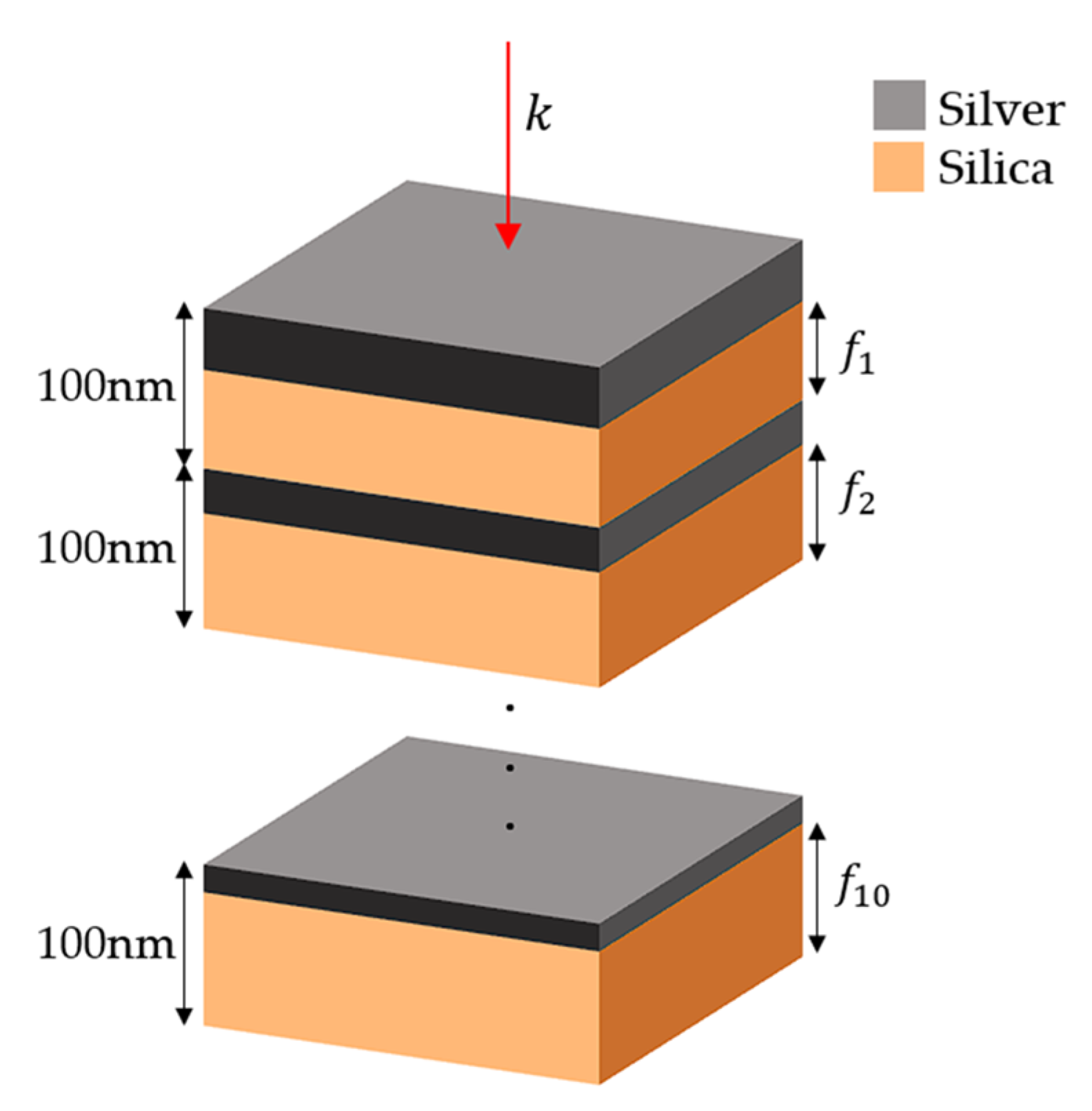
Figure 1 provides a schematic representation of the planar MDM that forms the basis of our study.
In the modeling of the device, as illustrated in
Figure 1, each segment was set to a height of 100 nm. The primary geometrical input parameter for this configuration was the dielectric filling fractions (fn) of each segment, defining the proportion of dielectric material in each 100 nm segment. The device’s design comprised 10 such segments, each uniquely composed of a silver–silica mix [
19]. Additionally, the direction of electromagnetic excitation is represented by k. This modeling approach is in line with prior studies on similar MDM structures [
20], allowing us to explore different design methodologies for these configurations and their implications for device performance.
The interaction of electromagnetic waves with a metal–dielectric interface that results in a phase shift, as described in [
21], is a particularly intriguing phenomenon in the context of structures engineered for broadband absorption and filter design. Such structures, when designed with strategically stacked metal–dielectric interfaces, offer a means to effectively control the resonances and, consequently, the overall optical behavior. This stacking arrangement allows for the precise manipulation of the wave interactions at these interfaces, thus enabling the tuning of the structure’s optical properties for desired applications. This controlled manipulation finds practical utility in the development of devices for photovoltaic applications [
3,
22,
23], where the efficient absorption and conversion of incident light into electrical energy are of utmost importance.
Furthermore, these engineered interfaces play an important role in the domain of color filters, where the manipulation of resonances facilitates the selective transmission or absorption of specific wavelengths of light. These interactions of electromagnetic waves within these structures may also find application in devices such as optical sensors, signal modulation, and controlled light emission processes. The design of these metal–dielectric interfaces not only contributes to a deeper understanding but also opens avenues for advancing the performance and efficiency of optical devices and energy-harvesting technologies.
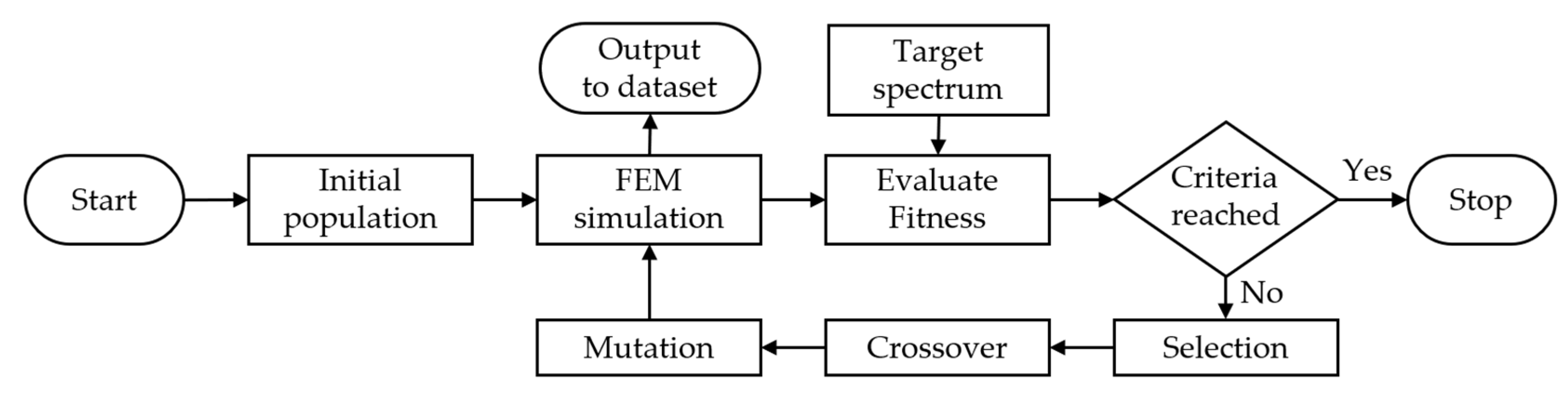
2.2. The Genetic Algorithm-Generated Dataset
The quality of the dataset used to train an ANN is fundamental for its generalization capabilities. A suitable dataset should include individuals with diverse characteristics in both geometric parameters (input) and optical properties (output). In this study, a genetic algorithm (GA) search routine (see
Figure 2) was employed to generate individuals for the dataset. We executed 65 different instances of the GA search to obtain reflectivity spectra in the visible band. A total of 65 target spectra were generated using a Gaussian function.
where
is the standard deviation, which is correlated with the full width at half maximum (FWHM), and
is the central wavelength, which was swept from 380 to 700 nm in 5 nm intervals. The simulated structures from the FEM that came up in the optimization process were added to the dataset.
As a paradigm of optimization grounded in the principles of natural evolutionary processes, GAs facilitates the systematic examination of a large number of potential solutions for a given problem. At each iteration of a GA, a mandatory step involves the evaluation of the performance of the device from the execution of an electromagnetic simulation for each individual to obtain its optical responses. The subsequent step involves a comparative analysis of these responses against the desired performance metrics through fitness calculations. The fitness function used in the GA optimization was the RMSE of the FEM-simulated spectrum of a given device under test and the target spectrum (Equation (1)) for that GA instance:
This dataset generation method inherently yields structures with similar geometries and optical behavior, given that the GA involves crossing over structures to produce new ones. To enhance diversity in the dataset and, consequently, reduce the computational time required to train the ANNs, redundant structures were filtered out. In this study, pairwise Euclidean distances between each individual in the dataset were calculated, and similar individuals were subsequently removed [
24,
25].
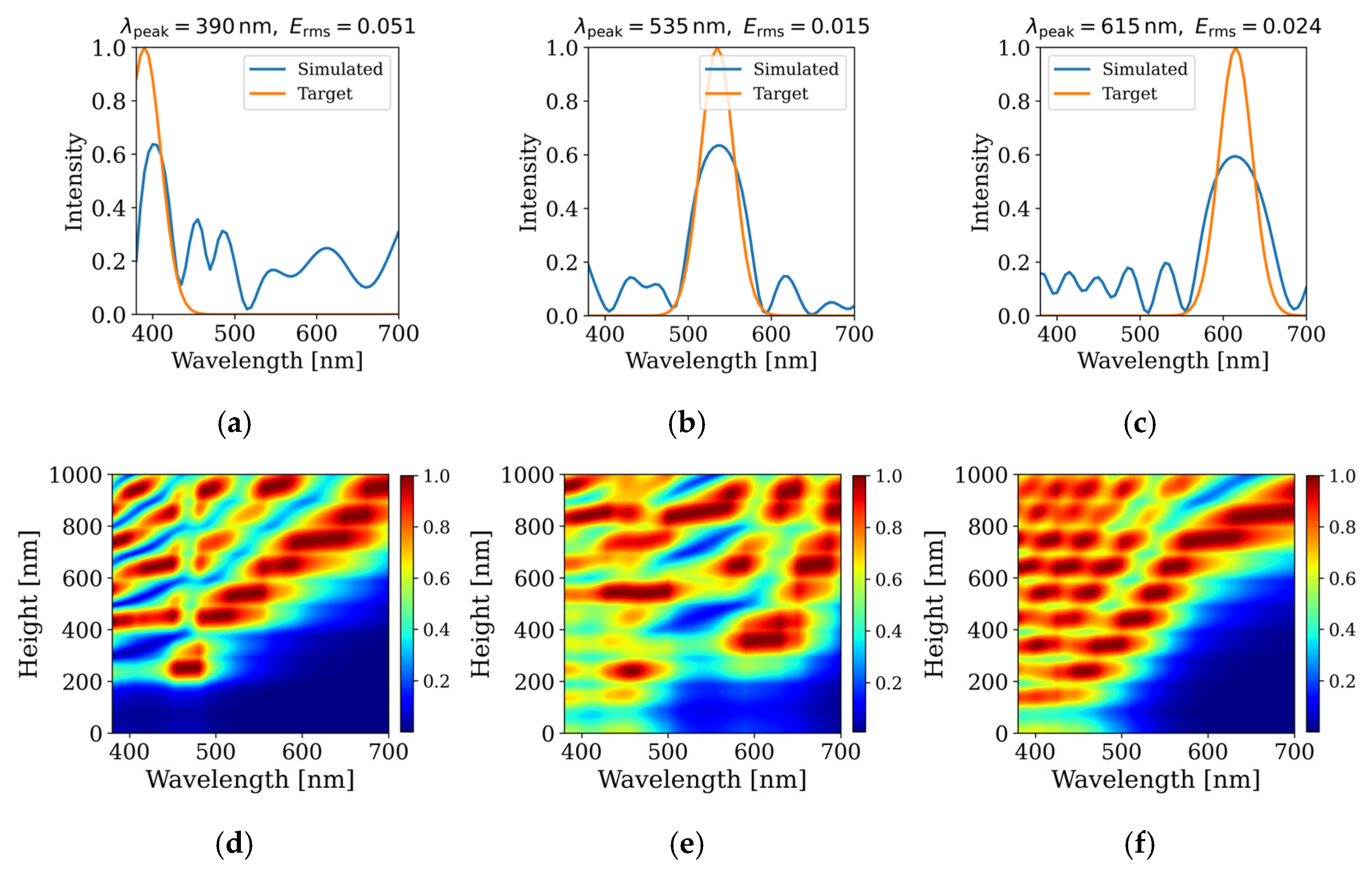
To illustrate the effectiveness of the genetic algorithm (GA) search, the outcomes are highlighted in
Figure 3, which shows the optimal solutions for wavelengths of 390 nm, 535 nm, and 615 nm.
Figure 3 also shows the field distribution along the proposed structure as a function of the position and the operating wavelength. The electric field is concentrated in specific regions depending on the operating frequency, which ultimately results in absorption. Complementing this,
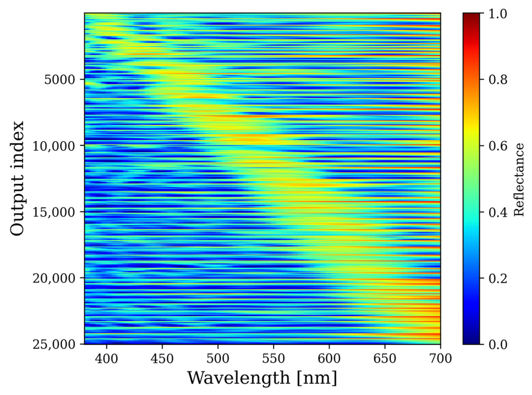
Figure 4 provides a detailed overview of the reflectivity spectra across the entire dataset, encompassing all 25,033 simulated structures, with a total simulation time of almost 37 h. A notable feature in these results is the diagonal profile of the reflectance peaks, which is a direct consequence of the sequential simulation process used during the dataset generation. This process began with a Gaussian-shaped target at a reflectance peak of 380 nm and methodically progressed through to 700 nm in increments of 5 nm, effectively mapping the spectrum’s response across this range.
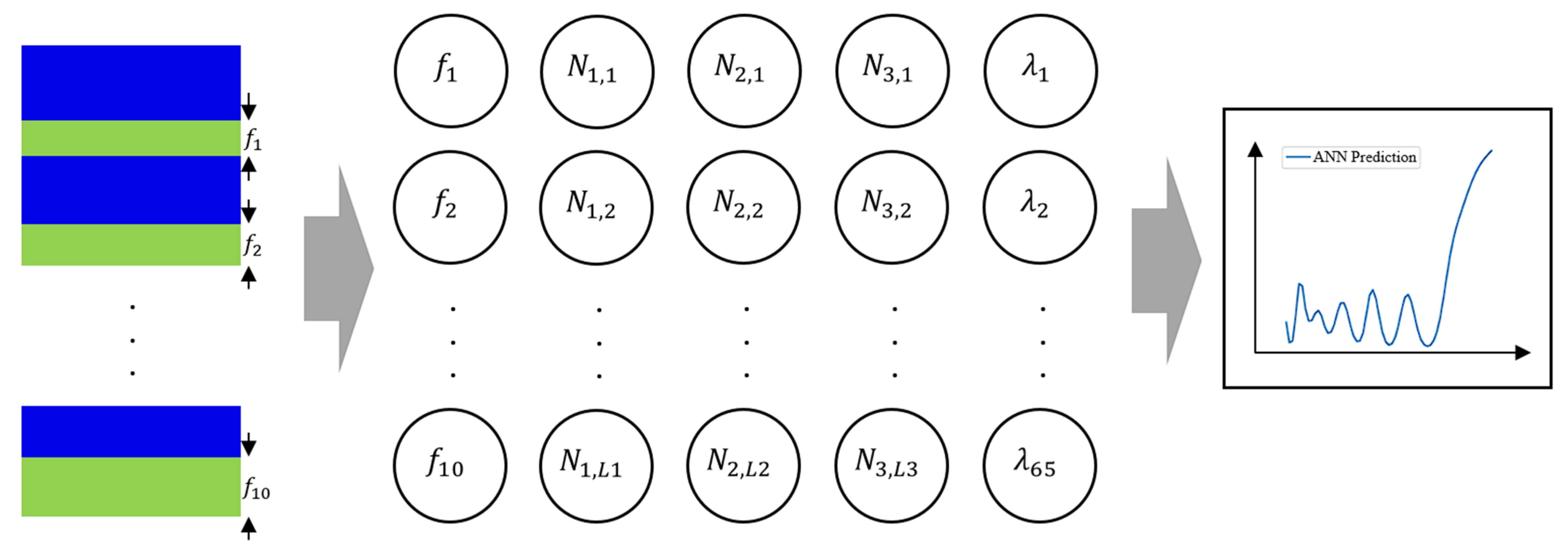
2.3. The ANN Architecture
The feedforward neural network—a fundamental architecture in ANNs, consists of an input layer, several hidden layers, and an output layer is a simple yet powerful structure that has been proven to be able to predict the optical behavior of photonic devices and find a range of applications as surrogate models [
2,
3,
4,
26]. The input layer is responsible for receiving input data, which, in our case, is the filling factor vector, and the output layer produces the predicted reflectance spectrum. The hidden layers process input through weighted connections and apply activation functions to produce intermediate representations, which are fed to the output layer, as depicted in
Figure 5.
The main feature of this approach to machine learning is the ability to progressively extract features from the training data, allowing the network to capture non-trivial input-output relationships. The training process involves the generation of an extensive dataset created by FEM simulations, which serve as ground truth for the iterative adjustments to neuron weights. The primary objective is to refine the network’s representation until it accurately mirrors the data distributions within the training set.
The artificial neural network (ANN) was implemented using the Python programming language and the TensorFlow module, a publicly available resource [
27]. TensorFlow’s top-level APIs were leveraged to streamline the process of defining and training the necessary machine learning architecture.
The appropriate size of an ANN is an optimization problem. A heuristic approach is commonly used to tackle this problem, such as systematically sweeping a set of combinations of layer sizes. We defined a configuration with three hidden layers as the basic architecture and tested different combinations of neuron counts in each layer, which are the hyperparameters, within a range of 10 to 300.
Expanding upon the ANN training process, it is essential to highlight the significance of optimizing hyperparameters for model generalization. While the architecture’s neuron count plays a crucial role, other hyperparameters, such as the learning rate and batch size, were also systematically explored to achieve the highest predictive accuracy. These hyperparameter adjustments were pivotal in ensuring that the ANN could effectively generalize its predictions beyond the training data, a critical requirement for its role as a surrogate model in the inverse design process. Furthermore, the fine-tuning of hyperparameters was conducted through a combination of manual tuning and automated techniques, such as grid search and random search, to identify the optimal settings for our specific problem.
The dataset was divided into three subsets, which were the training (60%), validation (20%), and testing (20%) subsets. The weights and biases in the ANN were adjusted via backpropagation using the training and validation subsets. The testing subset was used afterward to evaluate the performance of the trained ANN in unseen data, which was achieved by determining the mean correlation coefficient of the entire testing dataset ground truth with the ANN predictions.
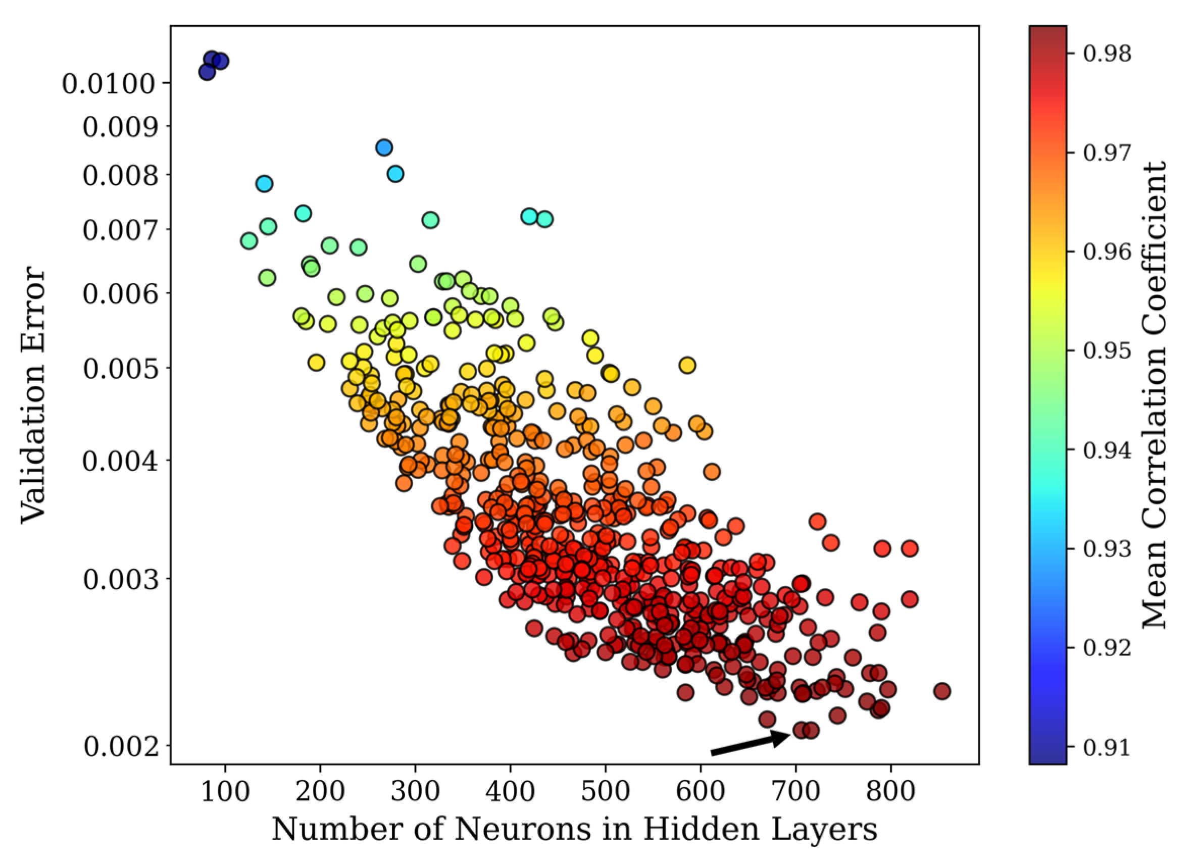
In
Figure 6, each point represents a trained ANN. Notably, the total neuron count exhibited a negative correlation with the validation error, reaching saturation between 600 and 800 neurons. The best performance of ANN demonstrated a maximum mean correlation coefficient of approximately 0.98, with 239, 211, and 256 neurons for the three hidden layers.
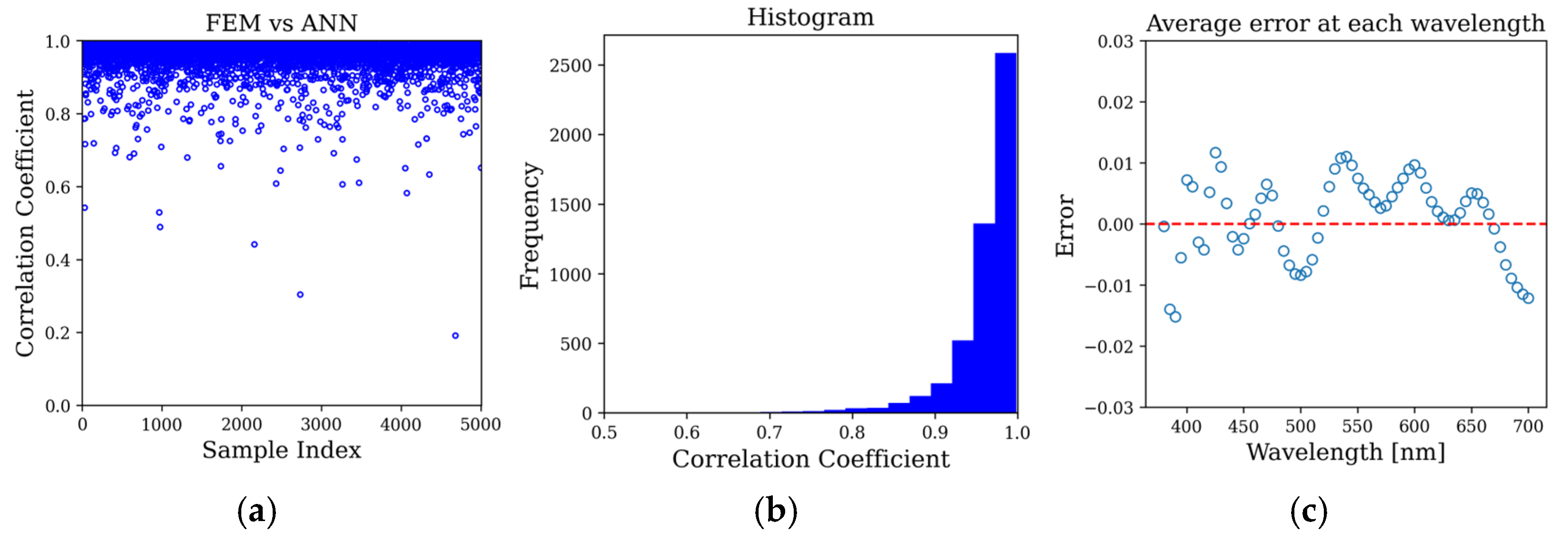
We calculated the correlation coefficient of the 5007 structures of the testing subset, as shown in
Figure 7. We also evaluated how the ANN’s predictions behaved with respect to its error for each wavelength, which is a performance metric that could have an uneven distribution. These results indicate that the model ANN suffices for its main purpose: to serve as a surrogate model for the FEM simulation.
2.4. Inverse Design
Our approach to inverse design was founded on the integration of a GA optimization loop with the meticulously implemented ANN, aimed at achieving precise target spectral behaviors. This step in the design process was made possible through the utilization of the PyGAD Python library, an open-source optimization and genetic algorithm implementation [
28]. In this context, the input of this system represents the desired spectral characteristics of the target, and the output is the geometrical configuration of the MDM.
In our methodology, we integrated a designer-configurable optical behavior into the fitness function, affording the freedom to select and define the desired behavior according to specific objectives. This chosen optical behavior serves as a guiding principle for the algorithm, driving the systematic exploration of parameter configurations with the goal of optimizing the device to closely approximate the specified target behavior. This approach proves exceptionally advantageous in scenarios where the parametric search space size is overwhelming. By incorporating this adaptable fitness function, we provide the means to efficiently manipulate the design space to achieve the desired performance characteristics.
The conventional way of testing the behavior of a given device by executing electromagnetic simulations makes use of substantial computational processing time, which becomes impractical given the size of the multiparametric search space. To avoid hindering the GA’s ability to find optimal solutions, a large number of individuals need to be tested, which may take a prohibitively long computer time. We substituted the electromagnetic simulation with the deployment of an artificial neural network (ANN) to overcome this computational bottleneck.
The transition to the ANN framework showcases its remarkable proficiency in efficiently capturing and generalizing the complex connections between the desired optical performance and the geometric parameters defining the target photonic device. By using the ANN, we can speed up the process of evaluating the structures by approximately 51-fold.
Table 1 summarizes the duration of the events in the process of simulation, prediction training, and generating the dataset using a conventional PC (Ryzen 1700 with 16 GB of RAM).
3. Results and Discussion
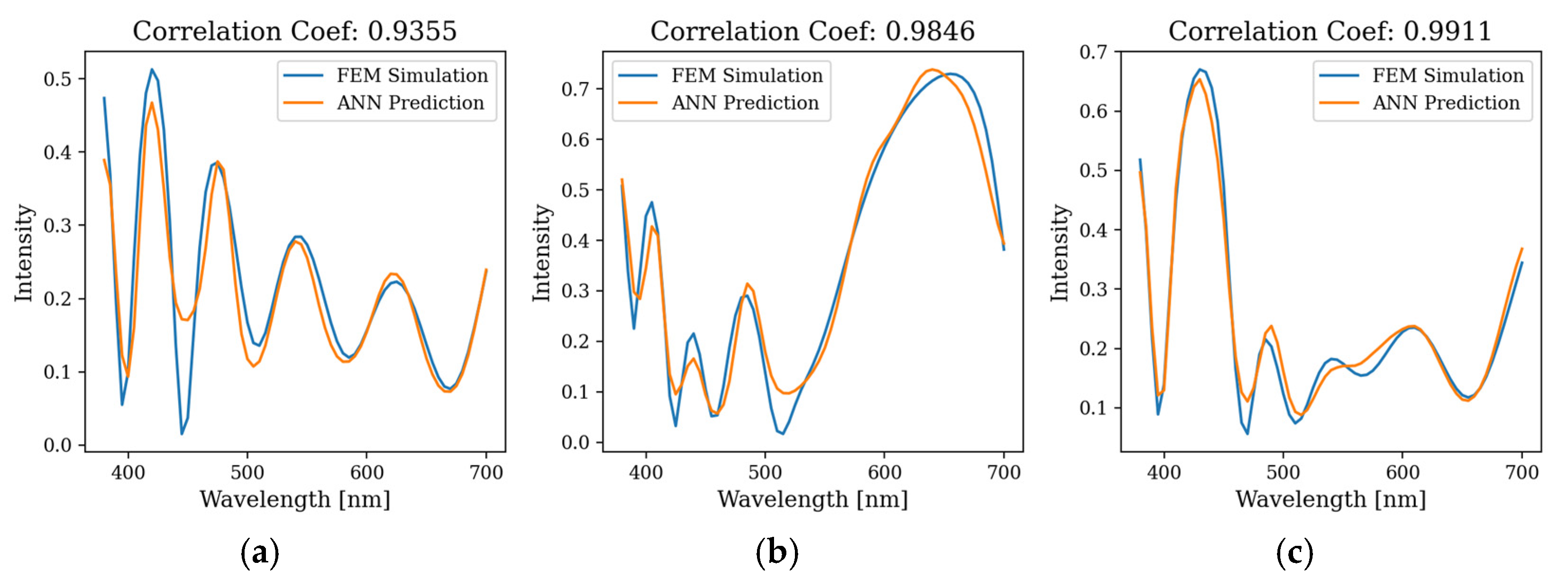
The trained ANN successfully predicted the reflectance spectra of arbitrarily provided geometrical inputs from the testing subset, demonstrating high values of correlation, as shown in
Figure 7, between FEM-simulated behavior and ANN prediction. We demonstrate the capabilities of the trained ANN in
Figure 8, where FEM and ANN spectra are compared with structures that were not present in the training phase of the ANN.
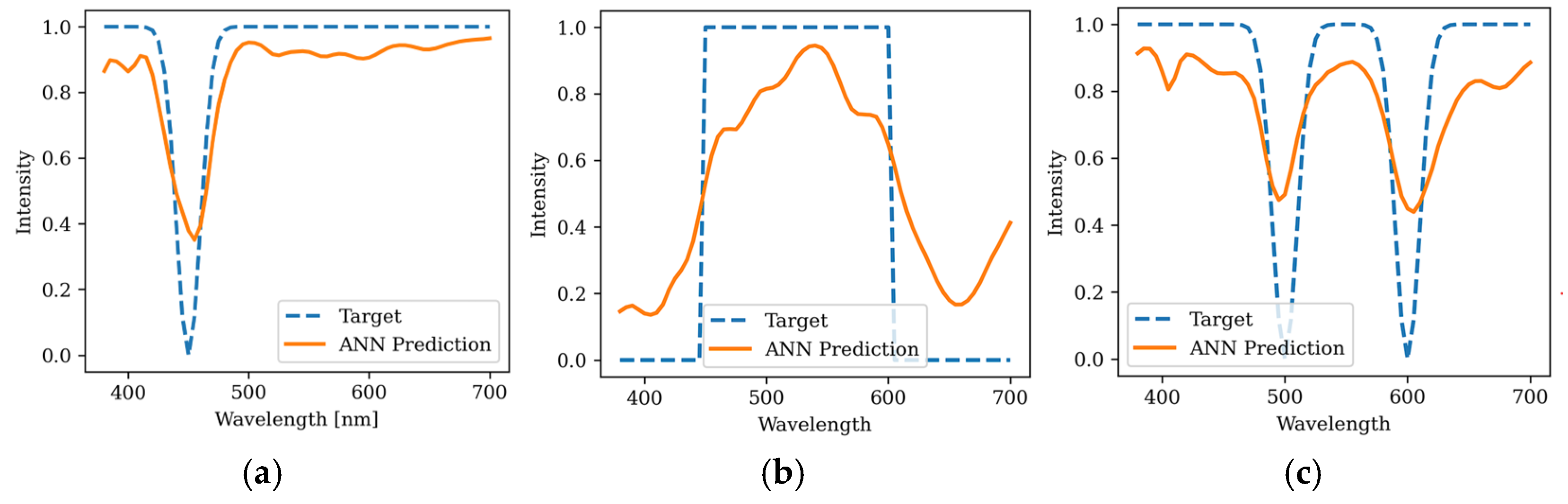
The trained ANN was effectively utilized as a surrogate model in the GA optimization loop using target spectra that were distinct from those included in the dataset generation, where only Gaussian-shaped target spectra were employed. As illustrated in
Figure 9, the GA routine successfully identified optimal structures designed to match notch, bandpass, and double-notch target spectra.
Table 2 contains the geometrical parameters for each optimal structure. It is noteworthy that these specific targets were not part of the original dataset used for FEM simulations, highlighting the exceptional ability of the trained ANN to extrapolate and predict novel structural configurations with high accuracy. This remarkable predictive capability underscores the versatility and effectiveness of the ANN as a powerful tool for inverse design in nanophotonics.
For each of the aforementioned target spectra that were not part of the training dataset, we executed a GA optimization loop spanning 100 generations, with a population size of 100 individuals in each generation. The computational time required for predicting the spectra using this setup amounted to approximately 17 min. This starkly contrasts with the alternative approach of relying on traditional FEM simulations for structure evaluation, which would have necessitated around 14.7 h of computation on a personal computer.
It is important to note that this time efficiency is achieved after an initial investment in creating the dataset and training the artificial neural network (ANN). The process of generating the dataset and training the ANN, essential steps in enabling the GA to function effectively, accounted for a substantial part of the total computational time. Despite this initial time investment, the efficiency gains become increasingly apparent when applying the trained model to new target spectra.
Although it is difficult to establish a comparison between different papers given the applications of deep learning to several optical devices with different properties, it is possible to use architecture complexity and the time simulation of model surrogates to position the results of this paper in the scientific literature. Compared with [
6,
7,
11,
12], in our paper, the results show that an ANN-MLP (multilayer perceptron) with three hidden layers presented an excellent correlation between ANN prediction and FEM simulation with a time that is approximately 51 times faster.
4. Conclusions
The proposed methodology leverages the synergy between a GA and an ANN surrogate model to inverse design a planar multilayer device for optical filtering that can be tuned to wavelengths in the visible band. In this work, we used FEM numerical simulations of MDM plasmonic structures to establish a comprehensive dataset to train the ANN. The results highlight the proficiency of the trained ANN in predicting reflectance spectra and its ability to generalize intricate relationships between desired performance and geometric configurations. The ANN predictions exhibit a high correlation of over 0.98 compared with ground-truth electromagnetic simulation while also achieving a computational speed that is approximately 51 times faster.
This study demonstrates the successful deployment of an ANN as a surrogate model in a GA loop, showcasing its ability to find optimal solutions for devices approximating targeted spectral behaviors. The trained ANN exhibits efficiency in predicting novel structures, as evidenced by the comparison of results based on FEM simulation and ANN-predicted reflectivity spectra for configurations that were not included in the initial training phase.
The focus on planar multilayered metal–dielectric structures is due to their relative simplicity and the feasibility of generating a comprehensive dataset for training the ANN within reasonable computational and time constraints. This focus allowed us to establish and validate our methodology effectively, demonstrating the powerful integration of AI in optimizing optical filtering devices. We fully recognize the potential of our methodology in the design of more complex, non-planar geometries.
Although the surrogate model depends on the generation of database training obtained from numerical simulations, a process with significant computational cost, the advantage of the proposal is to replace the numerical simulations with an inexpensive surrogate model (trained model) that can provide the designer with the possibility of determining the parameters of an optical device in quasi-real time. Therefore, the presented methodology is a promising and effective approach for the inverse design of complex photonic structures with diverse applications in areas such as photovoltaics, color filters, optical sensors, and energy harvesting technologies.


