1. Introduction
The development of the next-generation sensing devices faces the challenge of guaranteeing rapid and efficient detection of multiple analytes in parallel, together with portability features, mainly related to mechanical stability, low power consumption, accessibility, and user-friendly interfaces [
1].
Biosensing technologies are commonly based on the interaction of a target molecule (analyte) with a specific receptor, properly immobilized on the surface of a sensor, which converts the analyte–receptor binding events into a measurable signal. Depending on the method of detection of the target analyte, biosensors can be categorized into a few common groups, such as optical, electrochemical, or mechanical-based sensors. In particular, optical detection platforms based on surface plasmon resonance (SPR) offer several advantages, including high sensitivity to refractive index changes in the local environment, multiplexing capability, photostability, label-free reading, and the ease of miniaturization [
2].
Among others, plasmonic metasurfaces (PMs) are widely applied as sensing platforms for the detection of contaminants and relevant (bio)markers and (bio)molecules for environmental, (bio)medical and food applications [
3,
4,
5,
6]. Indeed, dielectric/metal periodic structures allow surface plasmon resonances to be tailored by optimizing the surface topography, i.e., by changing the shape of the unit cell, tuning the lattice periodicity, and varying the crystal symmetry [
7]. Extensive efforts are addressed in providing effective improvements for reliable and cost-effective manufacturing solutions, enabling massive production of miniaturized nanostructured sensing devices suitable for hybrid integration with other components into portable platforms [
1,
8]. However, the challenge remains to find a balance between the desired theoretical efficiency of the PMs and the most suitable technique for combining adequate resolution, good reproducibility, and quality of the PMs’ structures. Nonetheless, nanofabrication methods allowing cost- and time-efficient runs of patterning large areas (wafer scalability) are highly desired in view of massive scaling-up, making their manufacture attractive both to academic research and industry [
9].
One of the most applied structures in plasmonics consists of a hybrid metal/dielectric metasurface made of periodically arranged gold nanohole array (GNA), offering the possibility of controlling the light coupling with both propagating surface plasmon resonances and localized surface plasmon resonances [
8,
10,
11,
12]. Its main advantage relates to its simplicity in tuning and adjusting the spectral properties according to the structural parameters of the holes in the array, as well as to its metal-layer properties [
11,
12,
13]. Indeed, the symmetry of the structure, shape, dimensions, and spacing of the holes, together with the thickness of the gold layer, are important parameters that can affect the optical properties and then the sensing performance of the GNAs [
14]. PMs based on GNAs have been efficiently tested as biosensing platforms for several applications, like SPR [
8,
15,
16] and plasmon-enhanced fluorescence (PEF) [
17,
18,
19,
20].
In this framework, Plasmore Srl [
21] has developed a sensor based on GNA fabricated by resorting to a multistep approach, combining nanosphere lithography and plasma-based processes. The resulting PM consists of a hexagonal arrangement of polymer/air nanoholes, embedded in an optically thick gold layer deposited on a glass substrate. This PM has been demonstrated to be an effective high-performance biosensing platform in SPR and SERS applications [
16]. Successful preliminary trials have already been performed targeting multi-signal analysis by also resorting to PEF detection [
17]. In addition, a remarkable level of technology implementation into actual devices has been achieved and the PM has been successfully incorporated into a compact and monolithically integrated system for the detection of relevant milk-related analytes [
22]. Despite these valuable results, the actual fabrication protocol shows some disadvantages: limited number and size of the samples processable in parallel due to manufacturing equipment constraints and lack of in situ quality control during the different processing steps. This translates into time-consuming efforts, both in terms of personnel and materials, to guarantee reproducible PMs with high-volume production.
During the last decade, displacement Talbot lithography (DTL) has emerged as a promising manufacturing technique combining the requirements of high resolution, scalability, versatility, and ability to pattern substrates on large areas at relatively low cost [
23,
24,
25,
26,
27]. The DTL method is based on the use of a selected photomask and UV exposure to create patterns (such as 1D linear gratings, 2D arrays with hexagonal or square symmetry, and more complicated patterns) in a photoresist. This lithography technique relies on setting a specific Talbot distance, integrated into the diffraction field transmitted via a grating mask to obtain effectively patterned large areas, independently from the distance between substrate and mask. The resolution limit relates to the wavelength for the exposure, allowing a minimum pitch slightly below one-half of the wavelength to be achieved. The mentioned advantages of DTL make this method a promising route for a fast, robust, and scalable process in the manufacturing of a periodic PM like the GNAs.
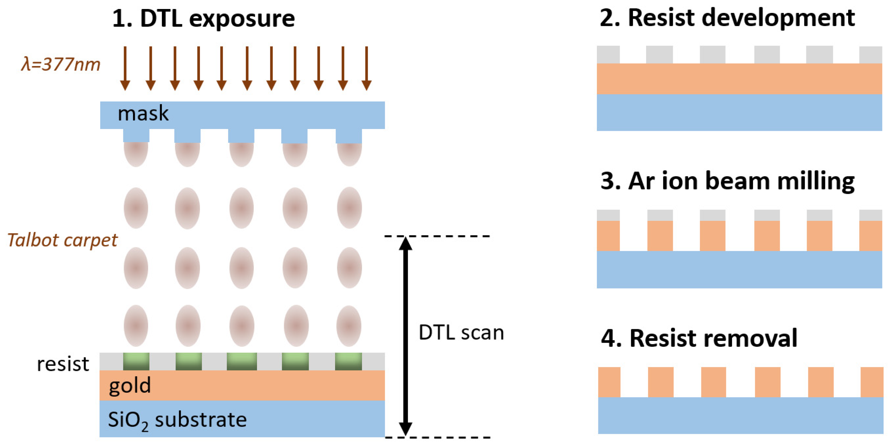
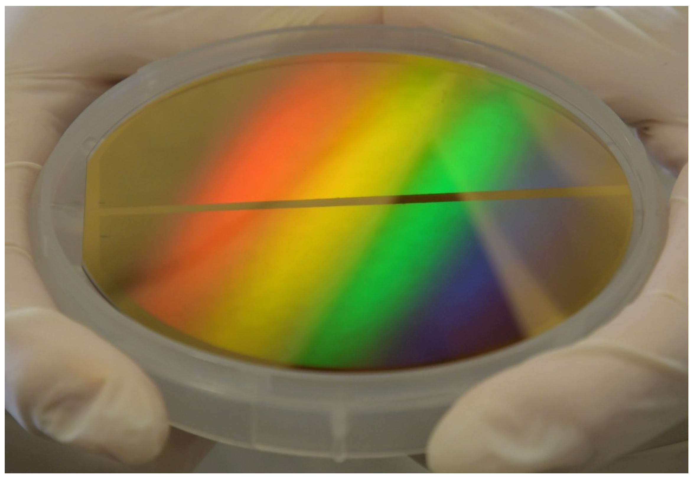
In this paper, we report the feasibility study carried out within the NFFA-Europe-Pilot project, aiming at realizing a PM based on a GNA utilizing a multistep lithographic method based on a novel joint usage of DTL and Ar ion-milling. DTL is used to develop the pattern on the resist onto the gold layer with a custom physical mask made using e-beam lithography. Then, an Ar ion-milling step is used to drill the holes in the metallic layer. While both DTL and Ar ion-milling are already established technologies, the combination of these techniques for the fabrication of wafer-scaled PMs is demonstrated here for the first time to the best of our knowledge, and it is able to guarantee a reliable and standardized optical response (
Figure 1). These PMs have been successfully designed and fabricated on a 100 mm glass wafer, assessing the requirement of industrial manufacturing scalability. It is worth noting how the diffraction pattern shown in
Figure 1 suggests the presence of a monocrystal, indicating high uniformity of the array pitch over the whole wafer, and thus assessing the scalability of the technique.
The optical characterization showed a response in the range of interest with localized plasmonic resonance in the near-infrared region. These surfaces were effectively probed for refractive index variations in a microfluidic cell, paving the way for their use as potential (bio)sensing platforms, as a valid substitute for the ones obtained using the limited multistep fabrication method used so far by Plasmore Srl.
3. Results
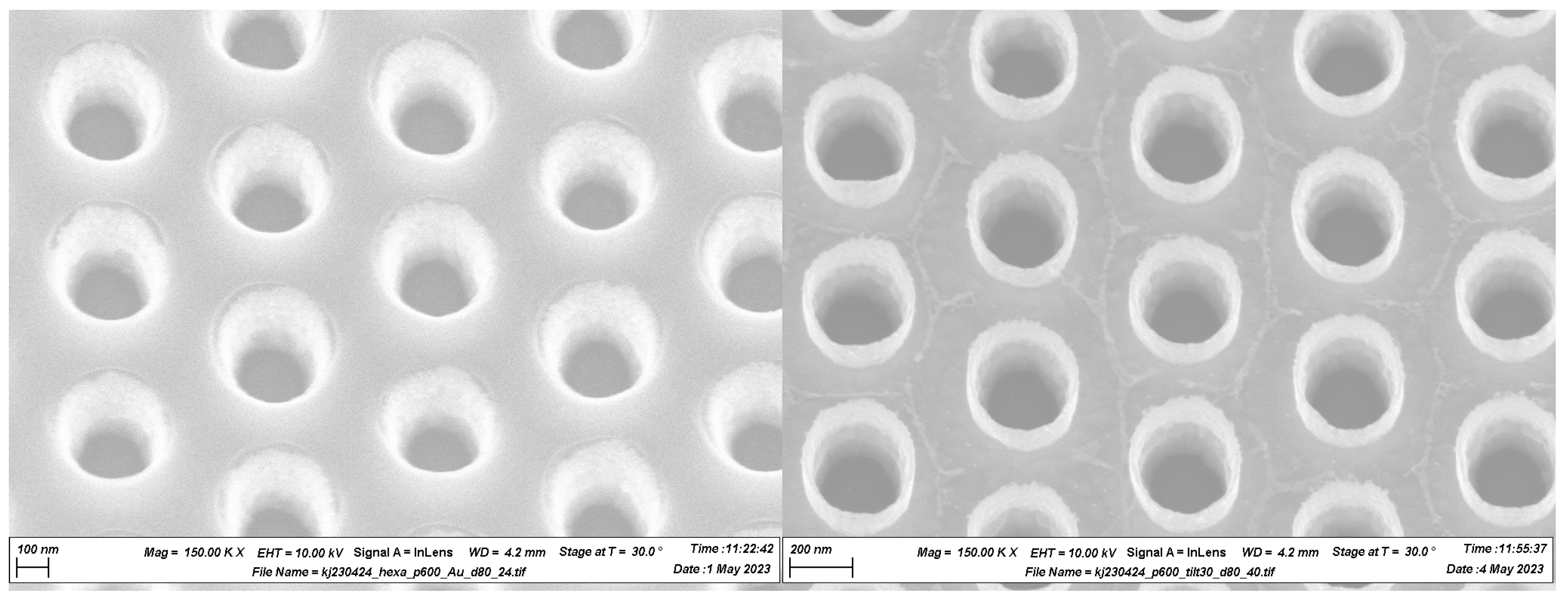
The resulting structures are shown in
Figure 3 before and after photoresist removal. One can observe two types of artifacts in the structures after the photoresist removal. The first type appears as some residuals between the holes. We believe they are related either to the redeposition of the material during the milling onto a surface of the photoresist mask or formed during plasma stripping during the plasma-ashing step. One cannot see the sign of these defects on the surface of the photoresist, however (see
Figure 3 left). In either case, one possible solution to avoid them is to strip the photoresist chemically. Another type of artifact appears as tube-like structures around the edges of the holes above the surface of the film. These are caused by the redeposition of the milled material onto the sidewalls of the photoresist milling mask. These structures appeared to be very hard to remove using Ar milling at oblique ion incidence angles. We assume that the reason for this is that these structures consist mostly of heavily carbonized gold, while carbon itself is one of the hardest materials to remove using Ar milling. These artifacts are inevitable consequences of the Ar milling process. We therefore decided to make our spectroscopic measurements on these structures as they are. One possible solution to reduce these artifacts in the future would be to use a hard mask or thin down the photoresist layer thickness to a minimum required.
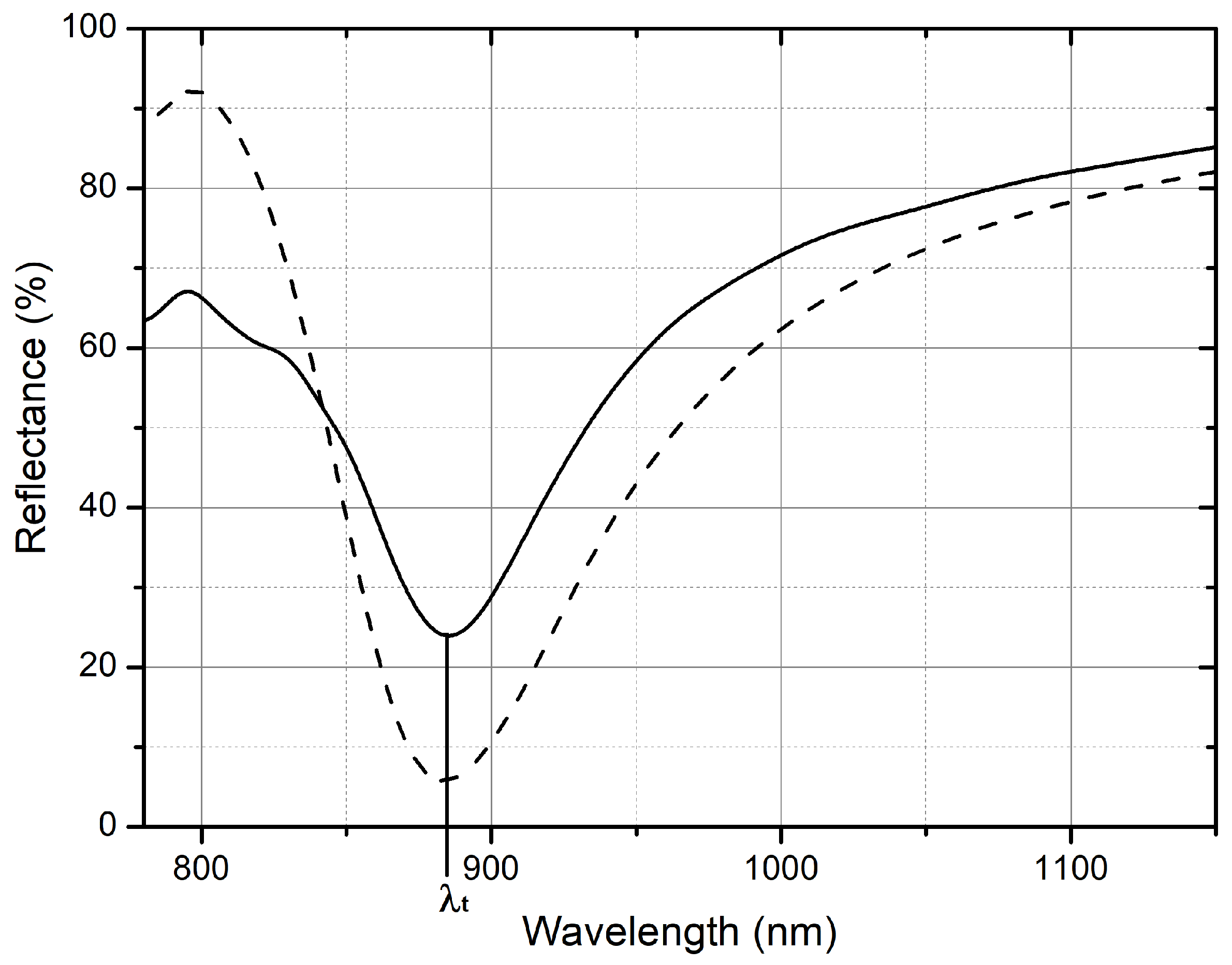
Figure 4 shows the measured R spectrum with a solid line, while the simulated R spectrum is shown with a dashed line. By using a customized particle swarm optimization algorithm implemented in the commercial software Ansys Lumerical FDTD (release 2023 R2.3, v8.30.3578) [
30], finite-difference time-domain (FDTD) numerical simulations were performed to optimize the PM to properly engineer the geometrical parameters and design the morphological features to finely tune its optical response within the near-infrared region, as reported in [
31].
As for the simulated curves, it is possible to notice an R maximum around 800 nm, showing the opening of a plasmonic band gap, strictly related to the pitch equal to 600 nm in a triangular lattice [
17]. The main plasmonic resonance is instead evident in the R spectrum as a dip at 885 nm, corresponding to the tuning wavelength (λt).
Measured and simulated spectra are in good agreement in terms of the position of the plasmonic bandgap and main localized resonance. The spectral shape and the position of the reflectance minimum are well retrieved by the simulations, while the minimum intensity is higher for the simulated data. The difference in the signal intensity can be attributed to a lack of thermal post-treatment, which results in a mechanical weakness and degradation of the gold–air interface.
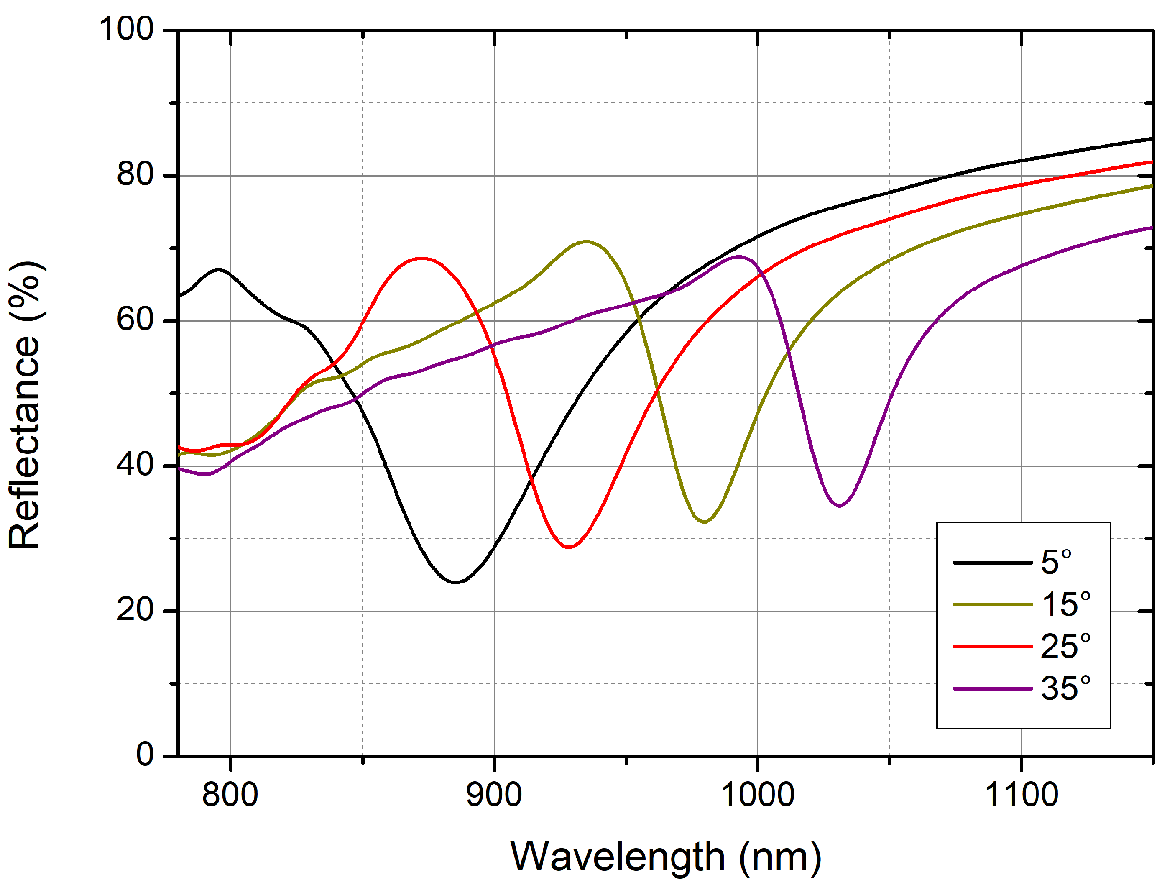
A deeper optical characterization of the main localized mode was carried out using angle-resolved reflectance measurements, with incidence angles varying in the interval between 5° and 35°. The lowest angle value was imposed by our setup, because it is the minimum angle of incidence that can be used; the highest angle was instead defined due to the dip wavelength position, which is too close to the upper detection limit of a standard silicon-based photodetector usually applied for (bio)sensing measurements in the near-infrared spectral range. The spectral position of the resonance dip shifted towards higher wavelengths as a function of the increase of the incidence angle, as reported in
Figure 5.
4. Discussion
The SEM images reported in the previous section allow for the interpolation of the structural parameters of the obtained PM. The diffraction pattern of the PM’s wafer shown in
Figure 1 indicates high uniformity of the array pitch, which strongly determines the plasmonic resonance position, thus suggesting the uniformity of the optical response.
The DTL technique allowed us to efficiently realize GNA metasurfaces tuned at the wavelength provided via a customized particle swarm optimization algorithm, previously implemented and employed in [
31]. Indeed, the resulting GNA is made on a gold layer with a thickness of around 80 nm and shows good reproducibility of the triangular lattice periodicity over the entire area of a 100 mm wafer, with a pitch of 600 nm and a hole diameter of around 200 nm. These features are in good agreement with the model introduced within the FDTD numerical simulations, where the pitch was set to 600 nm and the optimized hole diameter to 194 nm, resulting in the tuning wavelength at 885 nm. Near-normal incidence reflectance spectra show a high-quality optical response compared to standard colloidal lithography [
17] as well as e-beam or ion-beam lithography [
32,
33,
34], which are considered reference methods for periodic patterns such as PMs.
The angle-resolved reflectance spectra, acquired in the backside configuration, show dispersion of the localized plasmonic resonance, in line with the results reported for the standard nanofabrication technique in use so far by Plasmore Srl, assessing the consistency of the PM realized by means of DTL. This behavior suggests that reflectance measurements performed from the glass side of the sample are sensitive to refractive index changes at the opposite interface, even if the gold film is relatively thick. Moreover, the possibility of illuminating and collecting light from the glass side of the sample offers the advantage of easily interfacing it with a microfluidic cell, which is an essential requirement for biosensing applications. Indeed, to favor the interaction between analyte and receptor, the biomolecular assays are normally carried out in liquid.
To verify the effectiveness of the fabrication process, the detection capability of the PM under investigation was tested using a sensitivity measurement. The adhesion of molecules to the nanostructured surface is associated with a RI variation of the local environment. Due to the extreme sensitivity of surface plasmonic resonances to such a variation, it is possible to track the changes in their optical signature in R (i.e., the shift of the main resonance dip) as a tool for molecular detection, which is at the basis of SPR sensors [
16].
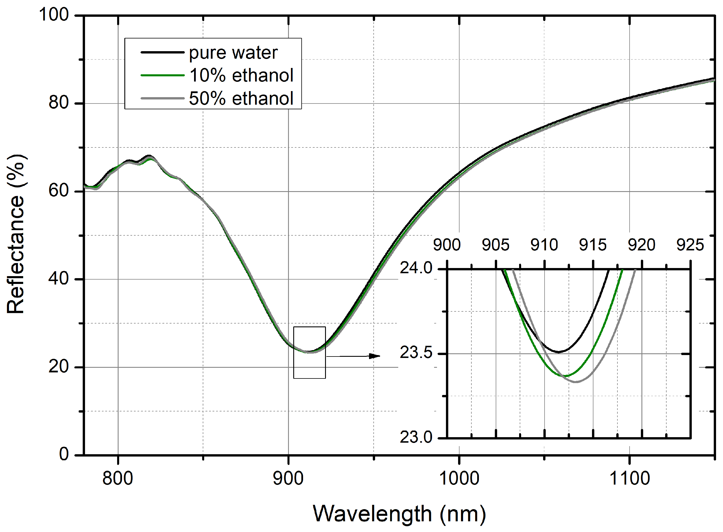
RI changes have been obtained by changing the EtOH concentration in a water solution. The results of the tests obtained with 10% and 50% EtOH solutions are shown in
Figure 6. If compared to the spectra reported in the
Section 3, it can be noticed that the reflectance minimum of R in water is red shifted with respect to the corresponding spectrum taken in air and the localized resonance dip moves to 912 nm. A further small red shift of a few nm also occurs when the RI of the liquid flowing on the surface of the PM is slightly increased, as in the case of 10% and 50% EtOH solutions. The detail of the R behavior around the resonance minimum reported in the inset of
Figure 6 highlights the red shift and the (small) intensity change of the R for the different EtOH solutions.
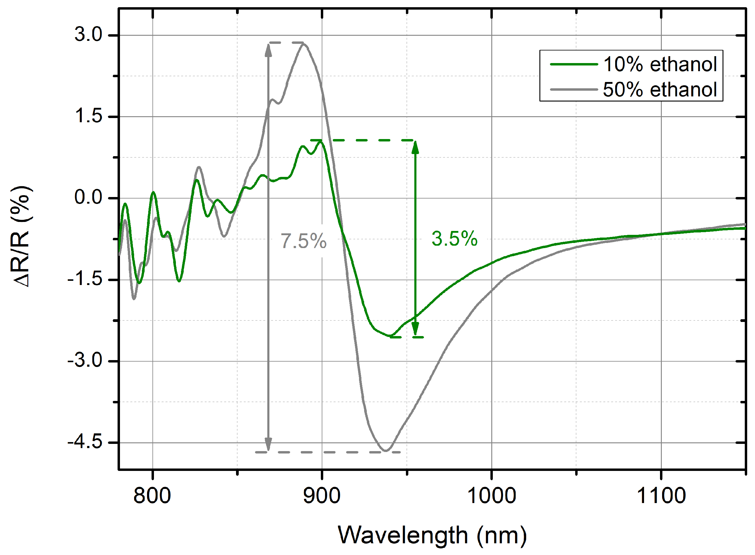
As an indication of the sensitivity, the collected reflectance data were analyzed to easily quantify the amount of signal variation and correlate it with the RI change. The relative variation (ΔR/R) was calculated as a percentage by considering the difference of the R values between the tested EtOH solution and pure water (ΔR = Rsolution − Rwater) and normalizing the obtained value to the R in pure water (Rwater). The graph of ΔR/R as a function of the wavelength is plotted in
Figure 7. It is evident that for increasing values of RI at the exposed surface, the reflectance variation shows two main regions around the wavelength of the localized mode, leading to a positive (increase in the reflectance intensity) and a negative peak (decrease in the reflectance intensity) for the smaller and larger wavelengths, respectively. The ΔR/R variation can be quantified as the peak-to-peak difference between the largest change occurring within those two regions. The total variation can be estimated to be roughly 3.5% for the 10% EtOH solution and 7.5% for the 50% EtOH solution, resulting in a variation of approximately a factor of 2.1 between the two solutions. These values can be compared with the RI changes of 8 × 10
−3 RIU and 2.1 × 10
−2 RIU measured for the two EtOH solutions, respectively. When a more concentrated solution is considered, the corresponding RI is roughly 2.6 times higher than the one corresponding to the solution at a lower EtOH concentration. The possibility of distinguishing this relative signal variation is in good agreement with RI changes and paves the way for the promising applicability of the presented nanofabrication to realize PMs meant to be applied as sensing platforms, thanks to their capability to measure small refractive index changes, as in the case of (bio)molecule detection.
5. Conclusions
In this paper, we reported the successful scaling up of a nanofabrication process to obtain tailored PMs for optical (bio)sensing applications. The study was carried out within the NFFA-Europe-Pilot project, aiming at realizing a PM based on GNA by a DTL manufacturing method, able to guarantee a reliable and standardized optical response. These PMs were based on a bidimensional triangular lattice realized on a gold layer deposited on a glass substrate and were meant to provide a valid substitute for the platform used so far by Plasmore Srl, characterized by a complex fabrication protocol resulting in time-consuming and low-volume production, in combination with limited reproducibility control.
Entering into details, the geometrical and morphological features were investigated using SEM, while the optical response was tested via fast Fourier transform spectroscopy. Microscopy characterization provided good agreement between the surface features (pitch, hole size, gold thickness) identified during the design and optimization steps.
On the other hand, the optical characterization showed a response in the near-infrared region of interest, characterized by a localized plasmonic resonance, well-tuned at 885 nm. Angle-resolved reflectance spectra, acquired by illuminating and collecting light from the glass back of the wafer, showed a dispersion of the localized plasmonic resonance, perfectly in line with the results previously obtained by Plasmore Srl with its standard nanofabrication technique based on colloidal lithography, assessing the consistency of the GNA realized by means of DTL.
To further verify the effectiveness of the fabrication process, the detection capability of small changes in the surrounding refractive index was tested through sensitivity measurements. Sensitivity tests were performed on two solutions with different EtOH concentrations in pure water by means of a customized microfluidic cell, which confirmed GNA competitiveness in terms of SPR-based probing efficiency. This paves the way for applying these GNAs as sensing platforms for the detection of biomolecular binding events, giving a successful chance for SPR sensors to finally reach the market.
A future plan for investigating this manufacturing method has been considered to verify the effectiveness application area with a specific interest in boosting their versatility, in view of the integration of this nanostructured surface into different miniaturized sensing devices. This is particularly interesting from the perspective of broadening the possible fields of application of the resulting structures, pushing the consequent technology transfer impact in cutting-edge technologies. Nonetheless, DTL might also be an alternative to more expensive lithography-based methods, in particular e-beam lithography, for fast prototyping purposes but also first approach purposes for new research-oriented proof-of-concept platforms.
By way of illustration, we are now targeting the understanding of the effect behind the reshaping of the nanoholes. This will require introducing a tapering angle able to manipulate the electric field coupling mechanism, introducing a specific directionality from the front GNA surface to the glass substrate back. In this way, the glass back can be used for both illumination and signal collection, defining a preferred direction of propagation for the electric field and allowing performing measurements in reflection geometry. In this way, the nanostructured front surface is completely available for functionalization and interfacing with the liquid to be analyzed, making the optimized PMs highly compatible with the best practice microfluidic requirements. Indeed, a signal acquisition configuration based on backside reflection is one of the more desirable features when engineering an optical SPR sensor for the detection of (bio)markers and/or (bio)molecules for environmental, (bio)medical, and food applications.

 ,
, 