Article

High Quality Factor Silicon Membrane Metasurface for Intensity-Based Refractive Index Sensing

1
Dipartimento di Ingegneria dell’Informazione, Università degli Studi di Brescia, Via Branze 38, 25123 Brescia, Italy
2
Istituto Nazionale di Ottica (INO)-Consiglio Nazionale delle Ricerche (CNR), Via Branze 45, 25123 Brescia, Italy
*
Author to whom correspondence should be addressed.
Optics 2021, 2(3), 193-199; https://doi.org/10.3390/opt2030018
Submission received: 3 August 2021 / Revised: 27 August 2021 / Accepted: 2 September 2021 / Published: 6 September 2021
(This article belongs to the Special Issue Feature Papers in Optics)

Abstract

:
We propose a new sensing device based on all-optical nano-objects placed in a suspended periodic array. We demonstrate that the intensity-based sensing mechanism can measure environment refractive index change of the order of 1.8 × 10 6 , which is close to record efficiencies in plasmonic devices.
Keywords:
sensing; metasurface; BIC

1. Introduction

Optical sensing has become very important in applications ranging from chemistry to biology, since it is a noninvasive approach and can provide a very fast response time [1,2,3]. In particular, metallic nanoparticles (NPs) have been extensively used for optical sensing because of their localized surface plasmon resonance [4,5]. Indeed, the latter property offers a strong enhancement of the electric field in proximity of the NPs, magnifying the system sensitivity to the environment refractive index changes. Hence, the nature of the analyte placed in proximity of the metallic NP can be disclosed by analyzing the sensor optical response. Recently, a plethora of sensors based on plasmonic structures have been presented [4,6,7] and proved to selectively detect cadmium ions and bacteria when jointly operated with optical fibers [8,9,10]. Although plasmonic sensors can offer a very good performance in terms of sensitivity, analyte selectivity and versatility, they may be plagued by strong ohmic losses due to light absorption in the metallic parts. This fact could yield an important temperature increase in the system, ultimately triggering unwanted chemical reactions or altering the analytes, which may provoke serious consequences for inflammable detection of gases such as methane or propane. Keeping the sensor temperature under control, by avoiding Joule heating occurring in plasmonic devices, is also of paramount importance in biological applications since even temperatures below 80 C may cause permanent damages in in-vivo applications.
In order to contain the losses, a valuable alternative is the design of optical sensors based on dielectric materials [11]. Nanostructures made with dielectric materials with high refractive index support Mie-type resonances that provide localized field enhancement. This resonant behavior can be obtained in the spectral region where the optical absorption of the material is negligible. In this regard, optical sensing in the environment of all-dielectric nanostructures was reported in [12,13,14,15,16,17]. In particular, silicon nanoresonator-based biosensors with good sensitivity were devised. The latest results show that all-dielectric optical sensing—a relatively unexplored field up to now—is promising for the conception of new generation sensors.
In this context, we propose a new sensing device based on all-optical nano-objects arranged in a suspended periodic array similar to what was reported in [18]. In particular, we consider a metasurface made of two suspended sheets of nanocylinders (NCs) held together by crossed spokes and separated by a small air gap. The NCs are made of silicon, a material endowed with a high refractive index, a crucial feature for a strong electric field confinement, and characterized by well-established nanofabrication techniques. Unlike many of the proposed sensors in literature, our device is not based on the shift of the resonant wavelength but rather on the change of reflectivity at a single wavelength [19]. In the following, we show that a single wavelength approach leads to an improved sensitivity with respect to the refractive index in the surrounding environment. This approach is advantageous for applications since it does not require additional components such as the spectrometer and the broadband light source, which are necessary for a sensor based on the resonance spectral shift. The single wavelength approach and the possibility to suspend the sensor allows to immediately apply the metasurface as a cheap and compact pressure sensor in ultra high vacuum systems. Moreover, our sensor does not require a substrate and it can be placed anywhere.

2. Results and Discussion

The device studied here is represented in Figure 1 and is composed of two arrays of silicon NCs held together by thin spokes. We start our treatment considering simpler geometries, i.e., a metasurface of NCs suspended in air and one made by two NCs separated by a tiny gap. We show that introducing a gap is fundamental to improve the sensitivity. In order to achieve this goal, we perform finite element method simulations to engineer the device geometrical parameters and study their behavior when the refractive index of the surrounding medium changes.

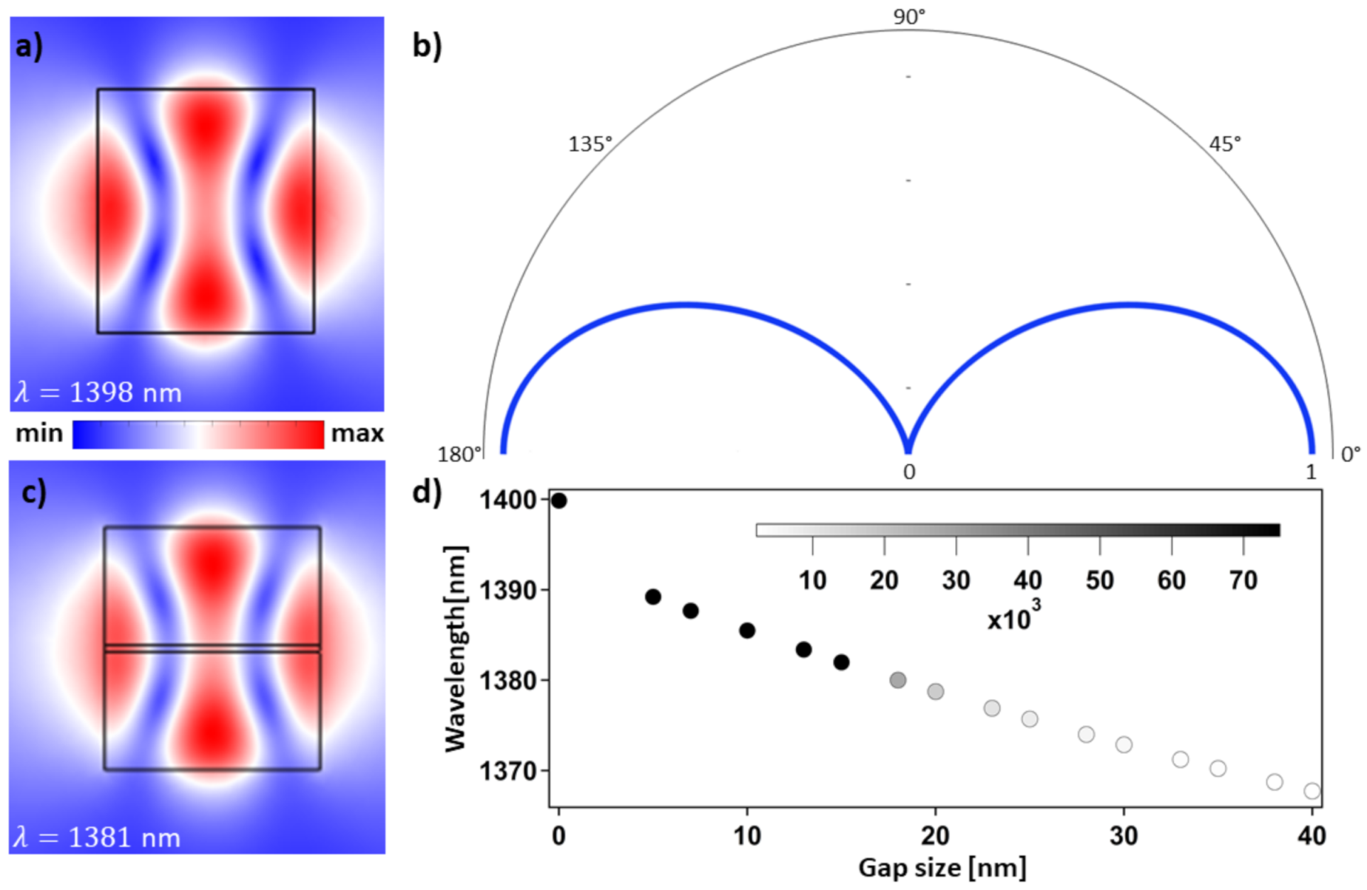
2.1. Metasurface Design

In order to achieve spectrally narrow resonances, we exploit quasi-bound states in the continuum (quasi-BIC). These are obtained from geometrical perturbations of BICs that are resonant states localized within the continuum radiation of the spectrum, yielding zero energy decay [20]. They were first introduced in quantum mechanics in 1929 by von Neumann and Wigner [21] and are now attracting a lot of interest in many fields of physics [20,22,23,24]. BICs are characterized by zero-linewidth spectral features, which is connected with the impossibility to directly couple with the impinging radiation. However, BICs are only a mathematical idealization, and in practice, we deal with quasi-BIC, which are characterized by a high but finite quality factor (Q-factor). We engineer a quasi-BIC starting from the eigenmode of a single isolated NC shown in Figure 2a. The related far-field radiation pattern is reported in Figure 2b, where it is clear that there is no emission along the vertical z-axis direction. This is due to destructive interference between the electric field radiated by the top and the bottom of the NC. In an infinite periodic array, when the periodicity is smaller than the mode wavelength, all the radiation channels, except the 0th diffraction order, are closed [22]. Since the mode is not emitting along the normal direction, as the isolated NCs become closer, the mode of the isolated NC evolves in a symmetry-protected BIC. In Figure 2a, the NC radius and height are 250 and 563 nm. The geometrical parameters of the metasurface, and consequently the BIC wavelength, were chosen by performing a parametric sweep in the range of dimensions accessible with well-established fabrication techniques for the most common dielectric materials [25,26]. The eigenmode wavelength can be arbitrarily tuned by changing the height of the cylinder. The eigenmode calculation for a single array of NCs suspended in air and periodicity P = 850 nm confirms that the selected mode is a BIC since the frequency imaginary part is zero. However, as explained before, it is not possible to couple to such a mode from a beam propagating in free-space and exploit very narrow features in the spectrum. To this goal, we introduce a 15 nm gap in the middle of the isolated NC (see Figure 2c). The gap in the NC induces a small phase shift along the vertical direction across the cylinder and thus the mode has finite radiation in the vertical direction. This enables the mode of the NC array to radiate in the (0,0) diffraction mode, transforming the BIC in a quasi-BIC. Hence, the modified geometry is now made of two arrays of NCs, separated by a small gap of 15 nm. The radius of the NCs is kept fixed at 250 nm, and the height of each NC is 274 nm. As a consequence, the height of the nanostructure with two arrays equals the height of the nanostructure with one array discussed before. The refractive index in the gap equals the one of the environment. We note that the gap size can be tailored to adjust the Q-factor of the mode by increasing or decreasing the interference between the field radiated from the top and bottom NC, as shown in Figure 2d, since it decreases when the gap size increases.
The electric field distribution with fixed period is almost unchanged and yields a finite, but very small, imaginary part of the eigenfrequency (see Figure 2d). Hence, it is possible to couple with an incident plane wave. Furthermore, the presence of the small gap in between the NCs is fundamental not only to couple light to the quasi-BIC but also for the operation of our sensor, since in order to maximize the sensitivity, the analytes to be sensed must be placed in a region where field confinement is strong.

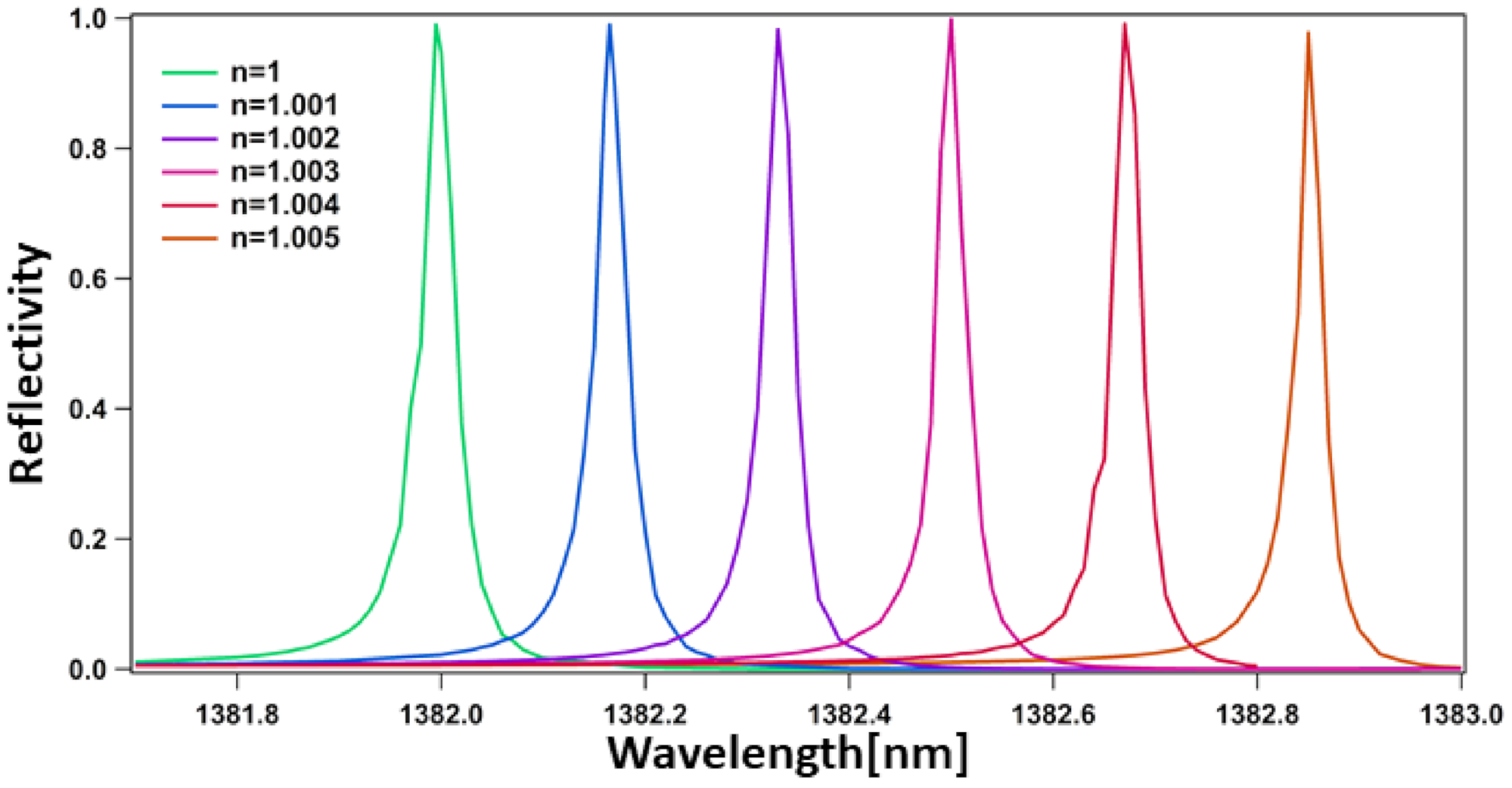
2.2. Sensing Mechanism

Once we have optimized the structure, we can analyze its sensing performance. The traditional sensing mechanism relies on the frequency shift of resonance as the environment refractive index varies. In this context, the sensitivity (S) is defined as [6,27]:
S = Δ λ r e s Δ n e n v ,
where Δ λ r e s is the shift of the resonant wavelength and Δ n e n v is the perturbation of the refractive index of the environment. In Figure 3, we report the spectral response of the sensor with double NC arrays without spokes as n e n v changes, and we obtain a sensitivity of 170 nm/RIU. This value is much lower than in plasmonic structures and comparable with previous results obtained in dielectric platforms [19]. Although the response is linear in the range 1 n 1.01 , the resonance shift is insufficient, resulting in limited sensitivity. However, in an intensity-based refractive index sensor, it is possible to exploit narrow resonances even if the wavelength shift is small. In analogy to [19], we define S I as:
S I = d R d n e n v ,
where we employ the metasurface reflectivity R instead of the scattering intensity, the latter being typically used to characterize isolated antennas. The device works at a single wavelength, and the surrounding refractive index is changed. We report in Figure 4 the reflectivity as a function of n e n v . For the case of a double NC array without spokes (black curve), the operating wavelength is 1382 nm, corresponding to the resonance for the nanostructure immersed in air. We highlight that the reflectivity halves for refractive index variations ∼1 × 10 4 (black line). According to our definition, S I is 5548 per RIU. In contrast to the traditional sensing mechanism, the intensity-based sensor is linear for a smaller range of refractive index variation. In the region 3 × 10 4 Δ n e n v 1 × 10 3 , the sensor response is not linear and the sensitivity reduces for larger refractive index perturbations. We note that highly sensitive sensors operating with the traditional mechanism have a similar linearity region with respect to refractive index variations [28].
Since we defined S in two different ways, depending on the sensing mechanism, in order to compare the two approaches and evaluate the sensor performance, we should consider the smallest appreciable variation of the refractive index that can be detected. High-end spectrometers can have resolutions of 0.1 nm, and the reported record sensitivity for a wavelength-dependent sensor is ∼ ( 140 ± 6 ) × 10 3 nm/RIU [28], which results in a minimum Δ n e n v in the order of 8 × 10 7 . With the same sensing mechanism, our device can detect Δ n e n v in the order of 6 × 10 4 . However, when the sensor operates in the intensity-based configuration, assuming a minimum measurable reflectivity variation of 0.01 , then the minimum detectable refractive index change by our device is 1.8 × 10 6 . It is worth noting that it is easier to experimentally detect reflectivity variations than wavelength shifts since this paradigm requires only a laser source and a photodiode.

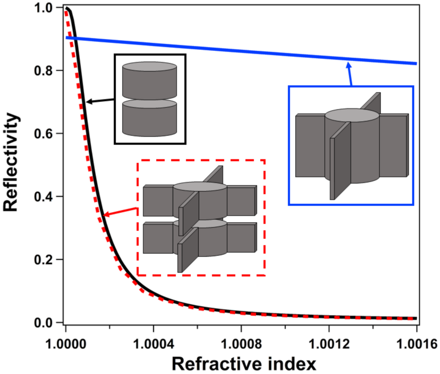
2.3. Practical Structure Design

For the sake of simplicity, up to now, we have considered arrays of free-standing NCs. However, these configurations are not experimentally realizable. To overcome this limitation, one may introduce four spokes per disk to sustain the silicon cylinders in air and achieve a geometry that can be fabricated and realistically employed. Each spoke has a rectangular cross section, whose height equals the one of each NC, and the width is 20 nm. (see Figure 1). One may expect that the spokes are enough to introduce a defect in the single NCs array and thus allow to couple the external radiation to the metasurface. However, as can be seen in Figure 4, the sensing performance of the single NCs geometry with spokes (blue line) is very poor compared to the double disk geometry (black line), which is almost unaffected by the introduction of the spokes (red dashed line). This comparison provides direct evidence of the importance of the air gap in the sensing mechanism, which is fundamental to exploit the high electric field enhancement inside the high-index contrast structures.

3. Conclusions

In this work, we designed a dielectric metasurface composed of two arrays of NCs suspended by spokes and numerically investigated their sensing application. We compared two different ways of operating the device, which are based on the resonant wavelength shift and the change of the reflectivity at fixed wavelengths, respectively. We demonstrated that the intensity-based sensing mechanism can measure the environment refractive index changes of the order of 1.8 × 10 6 , which is close to record efficiencies in plasmonic devices ( 8 × 10 7 ). We also prove the importance of the air gap between the two slabs to open a radiation channel that allows to couple the incident plane wave to the sensor by judiciously reducing the Q-factor and by also allowing to place the analytes in a region characterized by strong field confinement. Both these factors are fundamental since the introduction of the spokes, which are inserted in order to complete the definition of a fabricable device, is not enough to provide sensible variations of the reflectivity when the refractive index is changed.

4. Materials and Methods

All the simulations were performed employing the commercial software Comsol Multiphysics. The isolated NCs were simulated, introducing a spherical domain surrounded by perfectly matched layers and an eigenmode solver with a fixed refractive index n = 3.49 for silicon. The metasurfaces were simulated, imposing Floquet boundary conditions on the sides of the simulated domain and perfectly matched layers below and above the structure. We excited the nanostructures by using an impinging plane wave at normal incidence, and we changed the refractive index of the environment to investigate the sensing capabilities of the structure. The simulations of the incident linearly polarized plane wave take into account the dispersion of the silicon refractive index [29].

Author Contributions

D.R., M.G. and C.D.A. conceived the idea and supervised the study. A.T. and M.G. conducted the numerical simulations. A.T. wrote the manuscript. A.T., D.R., M.G., A.L., L.C. and C.D.A. contributed to the data analysis. All authors have read and agreed to the published version of the manuscript.

Funding

This research was funded by the European Commission grant number 899673, by the National Research Council Joint Laboratories program, Project No. SAC.AD002.026 (OMEN) and by Ministero dell’Istruzione, dell’Università e della Ricerca grant number 2017MP7F8F.

Institutional Review Board Statement

Not applicable.

Informed Consent Statement

Not applicable.

Data Availability Statement

Data are available upon request to the authors.

Conflicts of Interest

The authors declare no conflict of interest. The funders had no role in the design of the study; in the collection, analyses, or interpretation of data; in the writing of the manuscript, or in the decision to publish the results.

References

  1. Homola, J. Surface Plasmon Resonance Sensors for Detection of Chemical and Biological Species. Chem. Rev. 2008, 108, 462–493. [Google Scholar] [CrossRef]
  2. Mehta, B.; Benkstein, K.D.; Semancik, S.; Zaghloul, M.E. Gas Sensing with Bare and Graphene-covered Optical Nano-Antenna Structures. Sci. Rep. 2016, 6, 21287. [Google Scholar] [CrossRef] [PubMed]
  3. Pitruzzello, G.; Krauss, T.F. Photonic crystal resonances for sensing and imaging. J. Opt. 2018, 20, 073004. [Google Scholar] [CrossRef]
  4. Ruffato, G.; Romanato, F.; Garoli, D.; Cattarin, S. Nanoporous gold plasmonic structures for sensing applications. Opt. Express 2011, 19, 13164. [Google Scholar] [CrossRef] [PubMed]
  5. Gandolfi, M.; Banfi, F.; Glorieux, C. Optical wavelength dependence of photoacoustic signal of gold nanofluid. Photoacoustics 2020, 20, 100199. [Google Scholar] [CrossRef] [PubMed]
  6. Cheng, Y.C.; Chang, Y.J.; Chuang, Y.C.; Huang, B.Z.; Chen, C.C. A plasmonic refractive index sensor with an ultrabroad dynamic sensing range. Sci. Rep. 2019, 9, 5134. [Google Scholar] [CrossRef] [Green Version]
  7. Rodrigo, D.; Limaj, O.; Janner, D.; Etezadi, D.; de Abajo, F.J.G.; Pruneri, V.; Altug, H. Mid-infrared plasmonic biosensing with graphene. Science 2015, 349, 165–168. [Google Scholar] [CrossRef] [Green Version]
  8. Cai, S.; Pan, H.; González-Vila, Á.; Guo, T.; Gillan, D.C.; Wattiez, R.; Caucheteur, C. Selective detection of cadmium ions using plasmonic optical fiber gratings functionalized with bacteria. Opt. Express 2020, 28, 19740–19749. [Google Scholar] [CrossRef]
  9. Kumar, S.; Guo, Z.; Singh, R.; Wang, Q.; Zhang, B.; Cheng, S.; Liu, F.Z.; Marques, C.; Kaushik, B.K.; Jha, R. MoS2 Functionalized Multicore Fiber Probes for Selective Detection of Shigella Bacteria Based on Localized Plasmon. J. Light. Technol. 2021, 39, 4069–4081. [Google Scholar] [CrossRef]
  10. Liu, F.; Zhang, X.; Guo, T.; Albert, J. Optical detection of the percolation threshold of nanoscale silver coatings with optical fiber gratings. APL Photonics 2020, 5, 076101. [Google Scholar] [CrossRef]
  11. Baratto, C.; Faglia, G.; Carletti, L.; Angelis, C.D. New Trends in Optical Resonant Bio-Chemical Sensing. IEEE Sens. J. 2021, 21, 12856–12867. [Google Scholar] [CrossRef]
  12. Chong, K.E.; Orton, H.W.; Staude, I.; Decker, M.; Miroshnichenko, A.E.; Brener, I.; Kivshar, Y.S.; Neshev, D.N. Refractive index sensing with Fano resonances in silicon oligomers. Philos. Trans. R. Soc. Math. Phys. Eng. Sci. 2017, 375, 20160070. [Google Scholar] [CrossRef] [PubMed]
  13. Bontempi, N.; Chong, K.E.; Orton, H.W.; Staude, I.; Choi, D.Y.; Alessandri, I.; Kivshar, Y.S.; Neshev, D.N. Highly sensitive biosensors based on all-dielectric nanoresonators. Nanoscale 2017, 9, 4972–4980. [Google Scholar] [CrossRef]
  14. Muslimov, E.; Hugot, E.; Jahn, W.; Vives, S.; Ferrari, M.; Chambion, B.; Henry, D.; Gaschet, C. Combining freeform optics and curved detectors for wide field imaging: A polynomial approach over squared aperture. Opt. Express 2017, 25, 14598. [Google Scholar] [CrossRef] [PubMed] [Green Version]
  15. Rocco, D.; Tognazzi, A.; Carletti, L.; Baratto, C.; Angelis, C.D. Sensing through the optical radiation pattern in dielectric metastructures. In Proceedings of the International Conference on Quantum, Nonlinear, and Nanophotonics 2019 (ICQNN 2019); Dreischuh, A.A., Neshev, D.N., Staude, I., Spassov, T., Eds.; SPIE—International Society for Optics and Photonics: Bellingham, WA, USA, 2019. [Google Scholar] [CrossRef]
  16. Lu, X.; Gautam, V.; Shishmarev, D.; Daria, V.R. Sensing refractive index gradients along dielectric nanopillar metasurfaces. Opt. Express 2020, 28, 31594. [Google Scholar] [CrossRef]
  17. Tseng, M.L.; Jahani, Y.; Leitis, A.; Altug, H. Dielectric Metasurfaces Enabling Advanced Optical Biosensors. ACS Photonics 2020, 8, 47–60. [Google Scholar] [CrossRef]
  18. Kodigala, A.; Lepetit, T.; Gu, Q.; Bahari, B.; Fainman, Y.; Kanté, B. Lasing action from photonic bound states in continuum. Nature 2017, 541, 196–199. [Google Scholar] [CrossRef]
  19. Celiksoy, S.; Ye, W.; Wandner, K.; Kaefer, K.; Sönnichsen, C. Intensity-Based Single Particle Plasmon Sensing. Nano Lett. 2021, 21, 2053–2058. [Google Scholar] [CrossRef]
  20. Hsu, C.W.; Zhen, B.; Stone, A.D.; Joannopoulos, J.D.; Soljačić, M. Bound states in the continuum. Nat. Rev. Mater. 2016, 1, 16048. [Google Scholar] [CrossRef] [Green Version]
  21. von Neumann, J.; Wigner, E. Über merkwürdigediskrete Eigenwerte. Phys. Z. 1929, 30, 465–467. [Google Scholar]
  22. Koshelev, K.; Favraud, G.; Bogdanov, A.; Kivshar, Y.; Fratalocchi, A. Nonradiating photonics with resonant dielectric nanostructures. Nanophotonics 2019, 8, 725–745. [Google Scholar] [CrossRef]
  23. Hsu, C.W.; Zhen, B.; Lee, J.; Chua, S.L.; Johnson, S.G.; Joannopoulos, J.D.; Soljačić, M. Observation of trapped light within the radiation continuum. Nature 2013, 499, 188–191. [Google Scholar] [CrossRef] [PubMed] [Green Version]
  24. Campione, S.; Liu, S.; Basilio, L.I.; Warne, L.K.; Langston, W.L.; Luk, T.S.; Wendt, J.R.; Reno, J.L.; Keeler, G.A.; Brener, I.; et al. Broken Symmetry Dielectric Resonators for High Quality Factor Fano Metasurfaces. ACS Photonics 2016, 3, 2362–2367. [Google Scholar] [CrossRef]
  25. Staude, I.; Miroshnichenko, A.E.; Decker, M.; Fofang, N.T.; Liu, S.; Gonzales, E.; Dominguez, J.; Luk, T.S.; Neshev, D.N.; Brener, I.; et al. Tailoring Directional Scattering through Magnetic and Electric Resonances in Subwavelength Silicon Nanodisks. ACS Nano 2013, 7, 7824–7832. [Google Scholar] [CrossRef]
  26. Camacho-Morales, R.; Rocco, D.; Xu, L.; Gili, V.F.; Dimitrov, N.; Stoyanov, L.; Ma, Z.; Komar, A.; Lysevych, M.; Karouta, F.; et al. Infrared upconversion imaging in nonlinear metasurfaces. Adv. Photonics 2021, 3, 036002. [Google Scholar] [CrossRef]
  27. Liu, N.; Weiss, T.; Mesch, M.; Langguth, L.; Eigenthaler, U.; Hirscher, M.; Sönnichsen, C.; Giessen, H. Planar Metamaterial Analogue of Electromagnetically Induced Transparency for Plasmonic Sensing. Nano Lett. 2009, 10, 1103–1107. [Google Scholar] [CrossRef]
  28. Fusco, Z.; Rahmani, M.; Bo, R.; Verre, R.; Motta, N.; Käll, M.; Neshev, D.; Tricoli, A. Nanostructured Dielectric Fractals on Resonant Plasmonic Metasurfaces for Selective and Sensitive Optical Sensing of Volatile Compounds. Adv. Mater. 2018, 30, 1800931. [Google Scholar] [CrossRef] [Green Version]
  29. Green, M.A. Self-consistent optical parameters of intrinsic silicon at 300 K including temperature coefficients. Sol. Energy Mater. Sol. Cells 2008, 92, 1305–1310. [Google Scholar] [CrossRef]
Figure 1. Intensity-based sensing mechanism and the metasurface composed of two arrays of cylinders held together by thin spokes. When the analytes are not present, all the impinging light is reflected (a). If the refractive index of the surrounding medium is modified by the presence of gases, the light transmission increases according to the concentration (b).
Optics 02 00018 g001
Figure 2. Calculated eigenmodes by modal analysis for an isolated cylinder (a) and two suspended isolated cylinders separated by a 15 nm gap (c). The cylinder radius is 250 nm, the single disk height is 563 nm and the double disk height is 274 nm. Each field is normalized to the corresponding maximum value. (b) Electric far-field magnitude of the isolated cylinder associated with the mode in (a). (d) Eigenmode wavelength as a function of the gap size in a metasurface with periodicity 850 nm. We choose the periodicity in such a way that the resonant frequency of the isolated and periodic double disk geometries are similar. The color scale represents the quality factor.
Optics 02 00018 g002
Figure 3. Traditional refractive index sensing mechanism based on the resonant peak shift for different values of n. The peak shift ( Δ λ r e s ) linearly increases with the environment refractive index change ( Δ n e n v ). The graph is obtained for a double NC array without spokes and radius of 250 nm, height of 274 nm, gap of 15 nm and periodicity of 850 nm.
Optics 02 00018 g003
Figure 4. Intensity-based sensitivity. Reflectivity as a function of the refractive index of the environment at the resonant wavelength (obtained at n e n v = 1 ). The insets compare the unit cells of the three different metasurfaces to highlight the key role of the small gap between the disks: (Black) Periodic double disk arrays without spokes at λ r e s = 1382 nm. (Red) Periodic double disk arrays with 20 nm spokes at λ r e s = 1382 nm. The cylinder height is 274 nm, and the gap is 15 nm. (Blue) Periodic single disk array with 20 nm spokes and height of 563 nm at λ r e s = 1410 nm. The radius and periodicity are set to 250 and 850 nm, respectively.
Optics 02 00018 g004
Publisher’s Note: MDPI stays neutral with regard to jurisdictional claims in published maps and institutional affiliations.

