Review

Machine Learning-Assisted Optical Characterization and Growth Modulation of Two-Dimensional Materials

Hunan Key Laboratory for Micro–Nano Energy Materials and Devices, School of Physics and Optoelectronics, Xiangtan University, Xiangtan 411105, China
*
Authors to whom correspondence should be addressed.
Chemistry 2025, 7(3), 80; https://doi.org/10.3390/chemistry7030080
Submission received: 3 April 2025 / Revised: 1 May 2025 / Accepted: 7 May 2025 / Published: 13 May 2025

Abstract

:
This review focuses on research on machine learning-enabled two-dimensional (2D) materials, exploring the progress and prospects of this interdisciplinary field. At a fundamental level, machine learning algorithms incorporate imaging systems to build highly accurate viewing frameworks for material analysis. Two-dimensional materials have a rich set of optical properties, including light absorption and emission, anisotropy, photoluminescence, and nonlinear optical effects, which machine learning can accurately understand through image characterization, spectral fusion, and quantitative analysis. Meanwhile, the preparation process and post-processing are key aspects in the growth regulation of 2D materials, and machine learning helps optimize the experiments by analyzing the growth kinetics for fine control. Related research has spawned many academic achievements, gradually penetrating electronics, energy, and other industrial applications. The innovation of imaging technology and the deepening of multidisciplinary integration are expected to unlock more emerging applications and expand the application boundaries of 2D materials.

1. Introduction

At the forefront of materials science, two-dimensional (2D) materials exhibit a remarkable array of special optical properties through their unique and extraordinary arrangement of atomic structures [1,2,3]. 2D materials have only a single or very few thick nuclear layers, and this special dimension gives them a very different optical behavior from other materials. During the research and application of 2D materials, variations in experimental conditions can lead to the production of different optical properties. During the growth phase, small differences in parameters such as temperature, air pressure, and precursor concentration can significantly affect the crystal structure, defect density, and interlayer stacking pattern of the materials. These variations reflect the sensitivity of the two-dimensional materials to the experimental conditions and reveal the intrinsic correlation law between the structure and properties of the materials. An in-depth study of these change mechanisms helps to optimize the material preparation process, provides theoretical guidance for the regulation of the properties of 2D materials, and promotes their application in the development of electronic devices, optoelectronic devices, and other fields [4,5,6,7].
Optical images captured or photographed by an optical microscope are the most convenient way to observe the optical properties of a material. Although an experienced experimenter can crudely compare and determine the optical differences between two samples from a visual sense. From the image itself, it is often possible to use information from the Red-Green-Blue (RGB) color channel or Hue-Saturation-Value (HSV) space of the optical image to distinguish and identify certain optical features of the 2D material. Meanwhile, powerful techniques represented by Raman, photoluminescence (PL), and nonlinear spectroscopy can provide rich information on the fine structure features of 2D materials. For example, when polarized light is incident along different directions, the unique structure of some 2D materials leads to significant changes in their light absorption and reflectivity, accompanied by some new optical features [8,9].
After obtaining optical images or spectral information through optical techniques, subsequent data processing is also very important for detecting the optical properties of 2D materials. The traditional method, based on experience, relies heavily on the expertise of the researcher, is influenced by subjective factors, and has disadvantages such as low accuracy, poor consistency, low efficiency, and high labor intensity. The introduction of machine learning techniques has opened up entirely new avenues for exploring the optical properties of 2D materials, significantly changing the research landscape in this field [10,11,12]. By constructing a material database and combining it with advanced machine learning algorithms, the structural and optical properties of 2D materials can be effectively predicted, and suitable experimental conditions can be screened for them to regulate growth patterns. With the help of machine learning technology, scientists can explore the diverse properties of 2D materials in terms of spectral response, light absorption, luminescence properties, and photovoltaic conversion efficiency with unprecedented ease, laying a solid foundation for the design and development of new photovoltaic materials [13,14,15].
Compared with the existing image analysis methods and 2D material characterization methods, the ML method can automatically process and analyze a large amount of image data, greatly improving detection efficiency and accuracy [16,17]. Li et al. used the K-mean algorithm to build a training model and used the KNN algorithm to automatically segment the images [18]. Hu et al. combined a layer thickness identification criterion with an image segmentation algorithm that can quickly and reliably identify thin WS2 samples [19]. Machine learning algorithms analyze optical microscope images to identify the types and characteristics of 2D materials, which helps to quickly predict their optical properties. Wang et al. used machine learning to construct a Gaussian regression model to optimize the synthesis conditions and predict the experimental results [20], providing theoretical support for the preparation of region-specific molybdenum disulfide. Lu et al. applied ML to explore the relationship between growth conditions and CVD formation of monolayer/multilayer molybdenum disulfide [21]. The realization of controlled layer preparation can effectively reduce the consumption of time and resources and further promote the practical application of molybdenum disulfide. In addition, by training and optimizing the model, the ML method can quickly identify the growth kinetics of 2D materials under different experimental conditions, and then regulate their growth patterns.
The deep integration of machine learning algorithms with advanced optical characterization techniques has revolutionized 2D materials research. Machine learning has significantly improved the analytical capability of multiple optical detection techniques, realized the precise identification of changes in the optical properties of 2D materials, and can accurately analyze the correspondence between complex spectral features and the optical characteristics of materials, and so on. Notably, machine learning also shows unique advantages in 2D material morphology regulation, which can feed back and optimize growth parameters to achieve precise regulation of material morphology. Compared with traditional methods, machine learning-assisted 2D materials research has dramatically improved analytical accuracy, identifying subtle structural features that are difficult to detect with traditional methods and short response times. Machine learning methods have powerful data processing capabilities and can mine potential constitutive relationships from massive experimental data. With the continuous optimization of algorithms and the continuous improvement of computing power, machine learning will play a more important role in the basic research, practical application, and industrial manufacturing of 2D materials, and promote the development of this field in the direction of intelligence and precision. This paper presents a systematic review of the recent advances and application prospects of machine learning techniques in the field of optical characterization and growth modulation of two-dimensional materials, as shown in Figure 1.

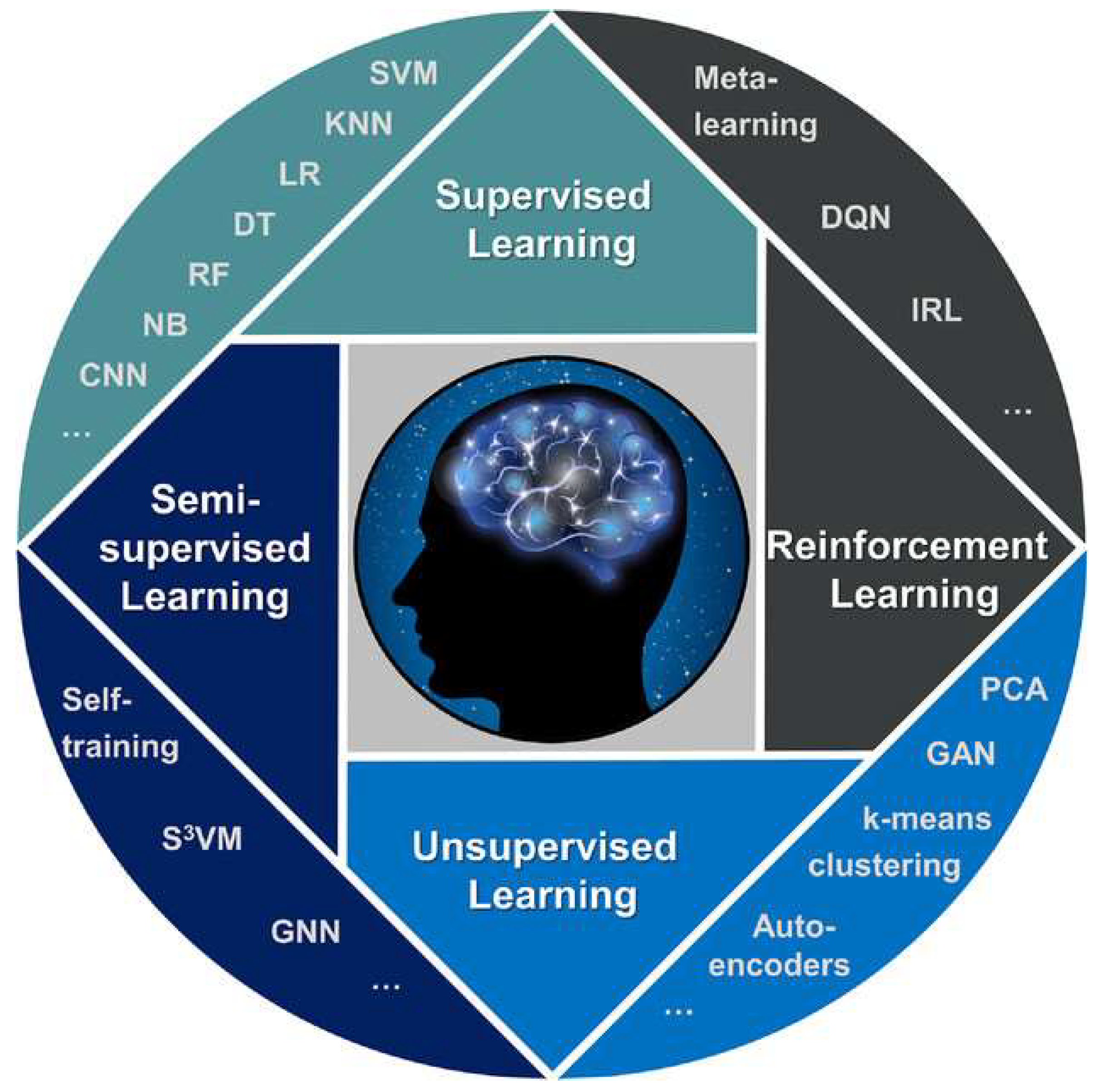
2. Machine Learning Fundamental Principles and Techniques

2.1. Machine Learning Algorithm Theory

Many algorithms that implement machine learning are based on statistical principles [22,23]. Depending on the training model, different learning methods can categorize machine learning (ML) into supervised, unsupervised, semi-supervised, and reinforcement learning. A brief overview of some typical ML algorithms is given in Figure 2. In supervised learning, the input data is considered “training data”, and each set of training data has a specific identification or result. In unsupervised learning, the data is not specifically labeled, and the algorithmic model infers the internal structure of the data. Semi-supervised learning has some of the input data identified and some unidentified and can be used for prediction. Reinforcement learning has the input data fed directly into the training model, and the model is adjusted in time. When data is entered into a computer, a general algorithm uses the data to perform calculations and then outputs the results [24,25]. The major difference with the general algorithm is that the inputs of the ML algorithm are the data and the desired result, and the output is the successful fuzzy algorithmic model, which converts the data into a result. Through machine learning, computers can generate their models and then provide relevant judgments to predict outcomes [26,27,28,29,30].
In supervised learning algorithms, classification and regression are two core tasks. Classification algorithms aim to classify input data into predefined categories, while regression algorithms attempt to predict one or more continuous values. Both types of problems rely on models learned from training data that achieve accurate predictions on new data by continuously tuning parameters to minimize prediction errors. Regression and classification essentially establish mapping relationships. The fundamental difference between them is whether the output space is a quantitative measurement space or a qualitative output space. The main job of a machine learning algorithm is to find decision boundaries and try to determine the best class based on a given input dataset. The learning algorithm also compares its output with the correct desired output and finds errors so that the model can be continuously improved. The commonly used supervised learning algorithms in 2D materials research are Support Vector Machines (SVM), K-Nearest Neighbors (KNN), Naive Bayes (NB), Decision Trees (DT), Random Forests (RF), Convolutional Neural Networks (CNN), and Gaussian Process Regression (GPR).
SVM excels in binary classification tasks and effectively handles multiclassification and nonlinear problems by introducing kernel tricks and multiclass classification strategies. The core of SVMs is to find an optimal hyperplane such that the two classes of samples are separated as much as possible and the distance (i.e., spacing) of the two classes of samples to this hyperplane is maximized. Support vectors are data points that lie on the decision boundary and are crucial for model construction. SVM improves the generalization ability of the model by maximizing the intervals, and for nonlinearly differentiable problems, maps the data to a higher-dimensional space utilizing a kernel function to make it linearly differentiable [32,33,34,35].
The KNN algorithm is used in both classification and regression but is more commonly used in classification tasks. At its core, it uses a distance metric (e.g., Euclidean distance) to find the K closest neighbors to a new instance in the training set. For classification problems, the class of the new instance is determined by the majority class of these neighbors; for regression problems, it may be the average of the objective values of these neighbors. The advantages of KNN are its simplicity and intuitive nature without the need for a training phase, but the computational cost increases significantly with the dataset and is sensitive to the scale and distribution of the data [35,36,37,38,39].
NB classifiers are based on Bayes’ theorem, which assumes that features are independent of each other. It classifies each category by learning its conditional probability distribution, calculating the a posteriori probability that a new instance belongs to each category, and selecting the category with the highest probability as the prediction. NB classifiers are computationally efficient and are particularly well suited for processing high-dimensional data, but the independence assumption limits their performance in certain complex scenarios [40,41,42,43].
DT is an intuitive classification and regression method that builds models by recursively partitioning the feature space. Each internal node represents a test on a feature, each branch represents a test result, and each leaf node stores a category (classification) or value (regression). Decision trees are easy to understand and interpret, but are prone to overfitting, especially when the depth of the tree is too large. Pruning techniques and integration methods, such as Random Forests, are used to alleviate this problem [44,45,46,47,48]. RF is an integrated learning method that improves the accuracy and robustness of a model by constructing multiple decision trees and synthesizing their predictions. Each tree is trained independently on a different subset of the training data, and the final prediction is derived from the predictions of all the trees by voting (classification) or averaging (regression). RF can reduce overfitting, has a good tolerance for outliers and missing data, and can assess the importance of features. However, its computational cost is relatively high, especially when dealing with large-scale datasets [49,50,51,52].
CNN, especially deep neural networks, have achieved great success in classification and regression tasks in recent years. They learn complex representations of data through multilayer nonlinear transformations and can extract features automatically without manual design. Neural networks optimize weights by backpropagation algorithms to minimize prediction errors. Though the training process may be time-consuming and require a large amount of data, once trained, neural networks are capable of handling a variety of complex pattern recognition and prediction tasks, including image recognition, speech recognition, and natural language processing. Different machine learning algorithms have their advantages and disadvantages, and the selection of an appropriate algorithm needs to be based on the nature of the specific problem, the size of the data, the computational resources, and the need for model interpretability [53,54,55,56,57,58].
GPR is a nonparametric probabilistic model based on the Bayesian framework, and its core idea is to directly model the probability distribution of predicted values instead of the specific functional form by assuming that the data obeys a Gaussian process distribution. The algorithm uses the kernel function to capture the similarity between data points and infer the mean and variance of the predicted values from the training data, which can efficiently balance the model complexity and data fitting in a small number of data scenarios. It is widely used in the fields of optimization, time-series analysis, and reinforcement learning [59,60,61].
Semi-supervised learning algorithms are in between supervised and unsupervised learning and are characterized by the simultaneous use of a small amount of labeled data and a large amount of unlabeled data for training in order to construct effective classification models. In practical scientific research, the acquisition of labeled data often faces challenges such as high cost, difficulty in labeling, or data scarcity, while unlabeled data is usually easy to obtain in large quantities. By combining a small amount of labeled data with a large amount of unlabeled data, semi-supervised learning aims to improve model performance by exploiting potential structural information in the data distribution. The model first learns initial decision boundaries based on labeled data and then fine-tunes the boundaries through intrinsic patterns (e.g., clustering assumptions, streaming assumptions) in unlabeled data (e.g., high-dimensional spectra, molecular dynamics trajectories, etc.). Typical approaches include Self-Training, Generative Adversarial Networks (GANs), and Graph Neural Networks (GNNs), which have shown significant advantages in areas such as materials discovery, bioinformatics, and quantum chemistry through pseudo-label generation, distribution alignment, or graph propagation mechanisms. However, the effectiveness of semi-supervised learning is highly dependent on the reasonableness of the data distribution assumptions and may face the risk of overfitting in strongly noisy or nonlinear systems, so the application scenarios need to be carefully selected with domain knowledge [62,63,64,65].
Reinforcement learning is a machine learning method that learns optimal strategies by interacting with the environment. Its core idea is to optimize behavioral strategies through trial and error and delayed reward mechanisms. During the learning process, the intelligent body adjusts its behavioral strategy by executing actions and observing the feedback (reward or punishment) from the environment, thus gradually approaching the optimal solution. Reinforcement learning is unique in its feedback loop mechanism, in which the intelligent body discovers which behaviors maximize long-term cumulative rewards through continuous experimentation and exploration. This approach allows a machine or software agent to autonomously learn and optimize behaviors to maximize performance in a given environment [66,67,68].

2.2. Machine Learning Model Building

In the field of machine learning, building an effective model involves several key steps and processes. Data collection is the basis for model construction, and the quality and quantity of data directly affect the performance of the model. Data can be derived from publicly available databases, experimental data, or simulation data, which typically contain various features such as structural, electronic, mechanical, and thermodynamic properties. For small datasets, migration learning, and data augmentation techniques can be used to scale the volume and diversity of data. Data preprocessing is an important step in ensuring data quality and includes data cleaning, removal of outliers and noise, and handling of unbalanced datasets to reduce bias and improve model robustness. Feature engineering is a core aspect of model construction, which involves extracting and selecting features from raw data that contribute to model learning. For image data, features may include color, texture, shape, and size. Whereas for spectral data, features such as peak, wavelength, and intensity may be involved. Effective feature engineering can map high-dimensional data to a low-dimensional space, reducing computational complexity while improving the model’s recognition rate and prediction accuracy. Choosing the right machine learning algorithm for model training is key. Commonly used algorithms include SVM, KNN, NB, DT, RF, CNN, and GPR. Each algorithm has its unique advantages and applicable scenarios, so it is usually necessary to train multiple models and evaluate their performance through cross-validation and error analysis. The general process of machine learning is shown in Figure 3.
Model evaluation is an important step to ensure the effectiveness of a model, and commonly used evaluation metrics include accuracy, recall, F1 score, Receiver Operating Characteristic (ROC) curve, and Area Under Curve (AUC) value. By comparing the evaluation results of different models, the most suitable model for a specific task can be selected. Moreover, visualization techniques, such as feature importance diagrams, decision path diagrams, or confusion matrices, can be used to intuitively observe the decision-making process of the model and to further optimize the model structure and parameters [69,70].
For classification models, accuracy is one of the most intuitive performance metrics, indicating the proportion of correct predictions made by the model. However, in datasets with imbalanced classes, Accuracy can be misleading because the model may be biased towards predicting the majority of classes. In this case, Precision, Recall, and F1 score are more applicable. Precision measures the proportion of instances where the model predicts a positive sample that is truly positive, and recall looks at the proportion of all truly positive samples that the model successfully predicts as positive. The F1 score is the reconciled average of precision and recall and is used to evaluate the model’s performance comprehensively.
The ROC curve and the AUC are other important methods for evaluating the performance of a classification model. The ROC curve demonstrates the performance of a model under different sensitivities by plotting the True Positive Rate against the False Positive Rate at different thresholds. The ROC curve shows how the model performs under different sensitivities by plotting the True Positive Rate against the False Positive Rate at different thresholds. The AUC value quantifies the area under the ROC curve, and a larger value indicates better model performance, which is especially suitable for model comparison when dealing with unbalanced datasets [71,72,73,74,75,76].
For regression problems, commonly used evaluation metrics include Mean Squared Error (MSE), Root Mean Squared Error (RMSE), and Mean Absolute Error (MAE). The MSE and RMSE consider the difference between predicted and true values of the squared error and give higher penalties for larger errors, while MAE directly calculates the mean absolute value of the prediction error and is more uniformly sensitive to errors [77,78,79,80,81].
In addition, the confusion matrix is a powerful visualization tool that provides a direct computational basis for metrics such as Precision, Recall, and Specificity, visualizing the model’s predictions across categories, making it easy to detect the model’s prediction bias in specific categories. Through the combined use of these assessment indicators and visualization techniques, it is possible to understand the performance characteristics of the model more comprehensively, identify potential problem areas, and then take targeted optimization measures, such as adjusting feature selection, modifying the model structure, or hyper-parameter tuning, to enhance the model’s generalization ability and practical application effects.

3. Optical Properties of 2D Materials

3.1. Light Absorption and Emission

The light absorption and emission processes in two-dimensional materials are closely related to their unique bandgap structure. In direct bandgap 2D materials, the top of the valence band and the bottom of the conduction band are at the same position in momentum space. When the photon energy is equal to or greater than the bandgap energy, an electron can jump directly from the valence band to the conduction band while absorbing a photon, which is known as the light absorption process. During light emission, an electron in the conduction band directly leaps back into the valence band, releasing a photon with an energy equal to the bandgap energy. The high probability of this direct jump makes direct bandgap 2D materials usually have strong light absorption and emission efficiencies. Single-layer transition metal sulfur compounds (TMDs), such as molybdenum disulfide (MoS2) and tungsten diselenide (WSe2), have a direct bandgap and exhibit remarkable photoluminescent properties in the visible range, making them potentially useful for applications in light-emitting diodes, photo-detectors, and other optoelectronic devices. As for the indirect bandgap two-dimensional materials, the top of the valence band and the bottom of the conduction band do not coincide in the momentum space. In the light absorption process, when the electron leaps from the valence band to the conduction band, the absorbed photon is needed to provide energy, and the phonon is needed to participate to satisfy the momentum conservation. Similarly, in the photoemission process, when an electron leaps from the conduction band back to the valence band, in addition to emitting a photon, it also requires the participation of a phonon. Due to the relatively low probability of phonon participation in the process, the light absorption and emission efficiency of indirect bandgap 2D materials is usually lower than that of direct bandgap 2D materials.

3.2. Optical Anisotropy

Some two-dimensional materials exhibit the phenomenon of optical anisotropy, i.e., differences in optical properties in different directions, due to their special structural characteristics. Taking black phosphorus as an example, its atomic structure is that phosphorus atoms form a pleated honeycomb structure through hybridization [82,83,84], which belongs to the orthorhombic crystal system. This structure makes black phosphorus have different electron cloud distributions, interatomic distances, and chemical bonding properties in different crystallographic directions. When light interacts with matter, the response to light varies in different directions, thus exhibiting optical anisotropy. There are significant differences in optical parameters such as light absorption coefficient and refractive index along the armchair and sawtooth directions of black phosphorus [85,86,87,88,89]. In-plane anisotropy is one of the most attractive properties of BP, providing another degree of freedom for the design of novel optical and optoelectronic devices. Jiang et al. directly observed and investigated the optical in-plane anisotropy of few-layer BP using scanning polarization modulation microscopy (SPMM) [90]. Polarization analysis and experiments showed that the SPMM signal was sinusoidally related to the polarization angle of the laser beam, thus determining the crystal orientation of the BP.
Optical anisotropy gives 2D materials a unique advantage in the field of polarized optical devices. As light with different polarization directions interacts differently with 2D materials, different photocurrent responses are generated, enabling the detection and analysis of polarized light [91]. In addition, it can also be used to manufacture polarized light filters, which can improve the accuracy of signal transmission and the clarity of images by reasonably designing the orientation and thickness of the material so that light in a specific polarization direction transmits and light in other directions is suppressed, which has important applications in the fields of optical communications.

3.3. Photoluminescence

The photoluminescence (PL) properties of two-dimensional materials, as one of the central characterizations of their low-dimensional quantum-limited effects, have attracted much attention in the fields of condensed matter physics and optoelectronics in recent years. Such atomic-thickness layered materials (e.g., transition metal sulfides MoS2, WSe2, black phosphorus, and graphene quantum dots) exhibit a unique optical response distinct from bulk phase materials when the radiative complexation process of electron-hole pairs is significantly modulated under light excitation. Single-layer transition metal disulfides (e.g., MoS2) exhibit strong exciton luminescence due to their direct bandgap properties, with quantum efficiencies of up to 10% and exciton binding energies of up to several hundred meV, and pronounced A-exciton and B-exciton emission peaks are observed even at room temperature. It is shown that the quantum-limited domain-induced direct bandgap transition (~1.8 eV) in monolayer TMDs leads to a fluorescence quantum yield enhancement of ~10⁶ times compared to that of the block and exciton binding energies as high as a few hundred meV (e.g., ~500 meV for WS2), which is much higher than that of the conventional semiconductors, which stems from the weakening of Coulombic shielding in the two-dimensional system and the high degree of anisotropy of the dielectric environment [92,93,94].
In addition, valley-selective luminescence (K/K’ valley polarization) can be achieved by circularly polarized optical excitation, laying the foundation for valley electronics devices. Wide bandgap materials like hexagonal boron nitride (h-BN) with defect-related single photon emission become important candidates for quantum light sources. The peak position, intensity, and polarization properties of photoluminescence spectra can also be used to accurately probe the number of layers, strain, and doping concentration of the material, which is a key means to characterize and modulate the optical properties of 2D materials. Further studies have shown that precise tuning of PL peak position, linewidth, and valley polarizability can be achieved by defect engineering (e.g., sulfur vacancy modification), strain gradient modulation, and van der Waals heterostructure building, providing a material basis for the construction of high-efficiency valley electronic devices and quantum light sources [94,95,96,97].
Recent ultrafast spectroscopic studies reveal that the 2D exciton-phonon coupling interaction dominates the non-radiative relaxation channel with the dark exciton state of the buoyant competition, which provides a new strategy to break through the conventional fluorescence lifetime limit (<1 ns). These findings not only deepen the understanding of the photophysical coupling mechanism of low-dimensional quantum materials but also open new paths for the development of next-generation flexible optoelectronic integration and quantum information processing devices [92,98].

3.4. Nonlinear Optical Properties

Two-dimensional materials such as graphene and materials other than graphene, including transition metal chalcogenides (TMCs), black phosphorus (BP), hexagonal boron nitride (h-BN), chalcogenides, topological insulators (TIs), and their heterostructures, show unique and diverse nonlinear optical responses. The optical nonlinearity of each 2D material has unique properties that can be used for specific photonic applications. Graphene is a widely studied nonlinear optical 2D material due to its broadband absorption at optical and terahertz (THz) frequencies, resulting from its almost zero bandgap nature. Other widely studied are TMCs. These are semiconductor materials with molecular formulae MX2 (MoS2, MoSe2, WS2, WSe2) and MX (GaSe, GaTe) known as Transition Metal Dichalcogenide Compounds (TMDCs) and transition metal monosulfide compounds, respectively. In these chemical formulas, M stands for transition metals such as Mo, W, Re, and Ga, and X stands for sulfur-based elements (e.g., S, Se, and Te). TMCs exhibit typical layer-dependent tunable band gaps ranging from 1 eV in the bulk or multilayer case to 3 eV in the single-layer (SL) configuration [99,100,101,102].
Several theoretical and experimental studies have predicted and demonstrated that the low band gap (e.g., MoS2 and WS2) exhibits a nonlinear optical response beyond the low-energy band gap (~1 eV). More specifically, BP is a thickness-dependent direct bandgap semiconductor that can be widely tunable between 0.3 eV (bulk) and 2 eV (SL). It bridges the gap between zero-bandgap graphene and relatively wide bandgap TMCs, making it suitable for broadband optoelectronic applications, especially in the infrared and mid-infrared regions. h-BN is another 2D material with a large bandgap of ~6 eV. It finds nonlinear optical applications in the UV to NIR region [103,104,105,106].
Two-dimensional materials exhibit nonlinear response behavior under the action of an intense light field, including nonlinear absorption, nonlinear refraction, and harmonic generation. These properties originate from the unique atomic layer structure and quantum-limited domain effect of 2D materials, which make them exhibit significant nonlinear effects in light-matter interactions. Materials such as monolayer transition metal sulfur compounds (e.g., MoS2, WS2) and graphene are capable of generating highly efficient nonlinear optical responses, such as second-harmonic generation (SHG) and third-harmonic generation (THG), under femtosecond laser excitation [107,108,109].
SHG and THG are high-harmonic generation processes in nonlinear optical effects, which involve the second and third nonlinear responses of materials to incident light, respectively. In two-dimensional materials, these nonlinear optical effects usually originate from asymmetric electron distributions and strong electron-photon interactions within the material. Their generation is dependent on the material’s intrinsic properties, energy band structure, exciton effects, and symmetry, affected by factors such as the material’s size, shape, and external environment. For 2D materials, their SHG and THG effects are closely related to the number of layers in the material. With the change in the number of layers, the electronic structure and symmetry of 2D materials change, which affects their nonlinear optical response. In single-layer 2D materials, the SHG effect is usually more significant due to inversion symmetry breaking. In contrast, in multilayer or bulk materials, the SHG effect may be suppressed due to interlayer interactions and symmetry restoration. Similarly, the THG effect is modulated by the number of layers, but its sensitivity to the number of layers may vary depending on the material type. These properties make 2D materials promising for applications in nonlinear optical devices, ultrafast photonics, and optical communications. In addition, by stacking different 2D materials to form heterostructures, their nonlinear optical properties can be further tuned, providing more possibilities for the design of novel optoelectronic devices. It will not be described in detail in this review [110,111,112,113].

4. Machine Learning for Optical Characterization of 2D Materials

4.1. Conventional Measurement Methods Based on Optical Properties

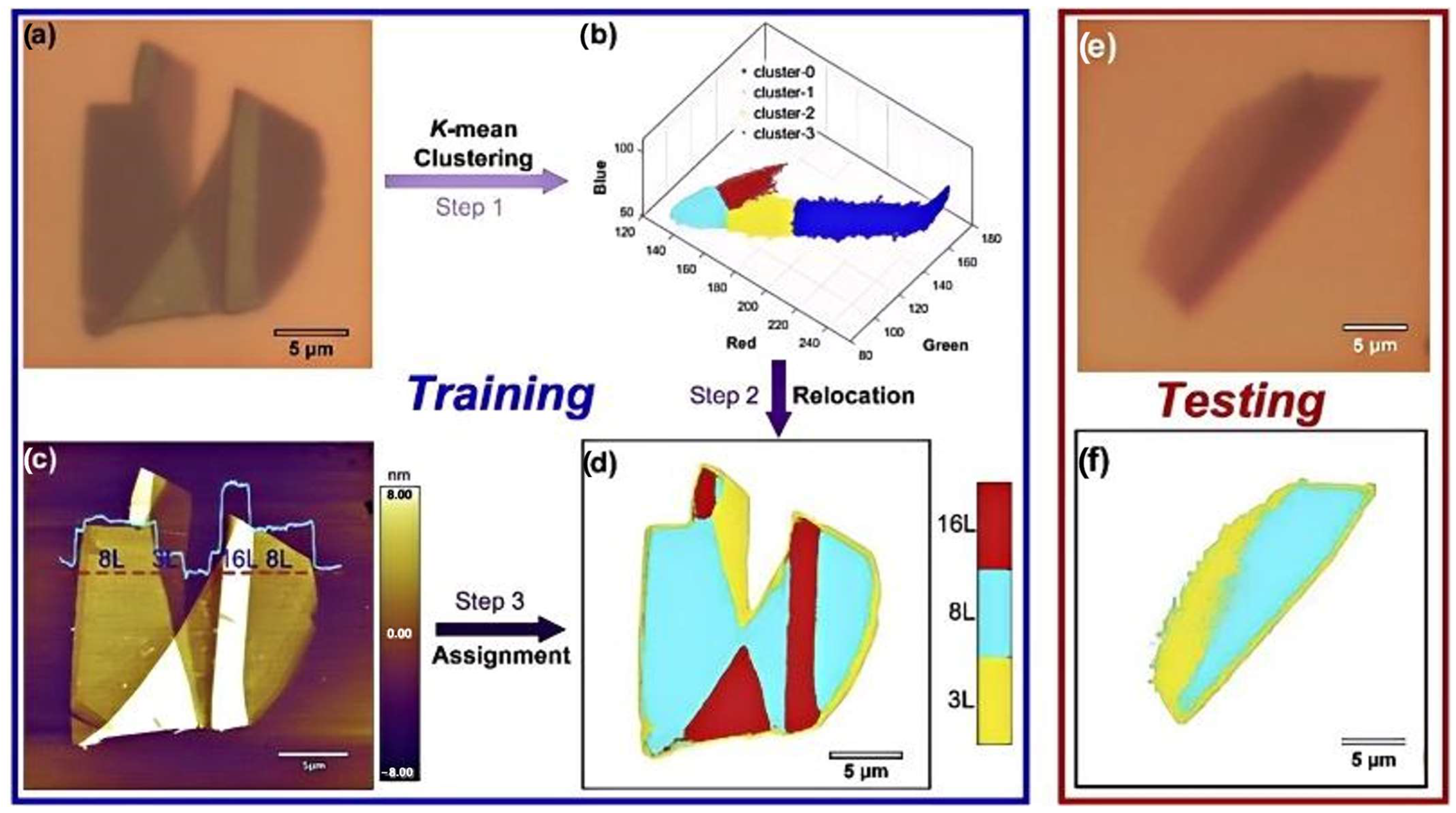
4.1.1. Optical Image

By saving the image under an optical microscope with a charge-coupled device (CCD) or complementary metal-oxide-semiconductor (CMOS) camera, it is possible to determine the average reflection at the interface between a two-dimensional material and air. The camera in an ordinary microscope can easily acquire each pixel’s R, G, and B values [114], which represent the average contrast value in its corresponding wavelength range, and indirectly the average reflection at the material-air interface and can be extracted by Python code. Mao et al. measured the angular optical contrast of a small number of BP samples on a 300 nm SiO2/Si substrate to quantitatively study the optical anisotropy of BP [115]. Optical contrast (δR) is the fractional change in reflection due to the presence of the sample on the substrate and is defined as in Equation (1):
δ R = R f i l m + s u b R s u b R s u b
where Rfilm+sub and Rsub are the reflection intensities of the sample and the blank substrate, respectively, and the scheme is shown in Figure 4a. Therefore, the average optical contrast of the BP samples was calculated in the RGB channel and plotted in Figure 4b. Since the contrast is directly related to the reflection intensity, it reproduces the cyclic variation, which is a clear sign of the optical anisotropy of the less-layered BP. The choice of RGB channels can be very different for different 2D materials and different substrates. High-contrast images extracted from the R channel were used to identify the number of MoS2 flakes on SiO2/Si substrates, whereas the B channel may be a better choice for transparent gel film substrates. These methods can effectively reduce the reliance on special experimental setups (light sources, expensive spectrometers, and detectors) and simplify the relatively time-consuming process of data processing.
Due to the different experimental configurations in different laboratories, the test results in terms of the light source, exposure time, white balance, color tone, etc., may also vary to some extent. Prakriti P. Joshi has imaged the nanoscale variation in the polarization-dependent photoemission response of BP using photoelectron emission electron microscopy (PEEM) [116]. At a spatial resolution of 54 nm, a ±20° phase shift in the polarization absorption was observed at the edges of the BP sheet compared to the interior of the sheet. By comparison with the DFT calculations, these phase shifts are attributed to changes in the symmetry of the occupied and unoccupied wavefunctions in and around the BP edges due to the one-dimensional constraints and symmetry degradation of the BP edges. The unique absorption properties of the BP edges mean that the extinction coefficients and complex dielectric functions of the BP edges are also unique within the sheet, which determines the functionality of the BP for on-chip photon, waveguide, and directional plasma applications. Edge-specific light absorption can also selectively excite nanoscale BP edges under far-field optical excitation, thereby controlling the spatial distribution of excited carriers on the nanoscale. Figure 4c shows a schematic of the experiment. Linearly polarized laser light is directed at near-normal incidence (NNI) via a Rh mirror onto a BP sample in a UHV PEEM microscope chamber (FOCUS GmbH). Not all edges of the thin section have the same phase shifts compared to the armchair orientation, but the phase shifts remain primarily the same along the entire edge segment. These phase shifts can be reproduced in different BP flakes and samples. The average phase shifts of short line segments from the edge of the lamella interior (⟨δβ⟩) were analyzed for the edge angle γ of five different BP lamellae and were found to be consistently phase shifted by as much as ±20° at the edge of the lamellae, although γ varied from 7° to 156° for different segments of the lamellae interior and the armchair orientation (Figure 4d). This work highlights how structural morphology can change the properties of two-dimensional materials as simple as light absorption, providing both challenges and opportunities for materials control.

4.1.2. Raman Spectroscopy

Raman spectroscopy plays an increasingly important role in the study of two-dimensional materials, revealing information about crystal structure, electronic structure, lattice vibrations, and sheet thickness, and can be used to probe strain, stability, charge transfer, stoichiometric change, and stacking order in materials. Spectroscopy consists of Raman modes at high and ultra-low frequencies and plays a crucial role in the study of 2D materials as a non-destructive method of spectral analysis. It can provide detailed information on the chemical structure, number of layers, charge doping state, stress, and strain state, and molecular interactions of 2D materials such as graphene, black phosphorus [85], hexagonal boron nitride, or transition metal disulfides (TMDs). Raman spectroscopy is also capable of detecting internal changes in the material due to charge doping or external stress and thus analyzing the doping type and stress state of the material. Meanwhile, by analyzing the characteristic peaks of Raman spectra, molecular vibration information, crystal structure, chemical composition, defects and impurities, and anisotropic features of 2D materials can be revealed, which is essential for understanding their physical and chemical properties. Resonance Raman spectroscopy has even been shown to be a good tool for studying the interactions between TMDs layers, revealing the complex physical phenomena between the layers.
In 2014, Xia et al. reintroduced BP as an anisotropic material with a narrow bandgap and high carrier mobility into the family of layered materials [84]. The x and y orientations of BP thin films were independently determined using angle-resolved DC conductivity measurements. For BP films thicker than 8 nm, flakes with lateral dimensions of tens of micrometers can be isolated, allowing the direction of crystallization to be determined using infrared spectroscopy. The lower right inset of Figure 5a shows an optical image of a BP flake with a thickness of about 30 nm. We measured the IR polarization-resolved relative extinction spectra (1–T/T0), where T and T0 are the transmittance of light through the BP and substrate and the substrate only, respectively. Figure 5a represents the 1–T/T0 measured on the BP with incident light coming from the Z direction at six different linear polarization angles, each separated by 30 degrees, which are represented by six arrow lines of different colors in the inset. In this experiment, 12 electrodes (1 nm Ti/20 nm Pd/30 nm Au) were fabricated on the same thin film. The electrodes were spaced at an angle of 30° along the direction shown in the inset of Figure 5b, which corresponds to the direction shown by the colored lines in Figure 5a. The same 0° reference is used here for the polarization-resolved IR spectroscopy measurements in Figure 5a. These DC conductivity measurements were performed by applying an electric field to each pair of diagonally positioned electrodes, which were 22 mm apart at 180°. The results are plotted in polar coordinates in Figure 5b. Measurements on each pair of electrodes resulted in two data points, positively biased and negatively biased, spaced 180° apart in Figure 5b. BP bridges the energy gap between semimetallic graphene and a variety of large-bandgap transition metal dichalcogenides (TMDCs), making the BP films ideal candidates for a wide variety of near- and mid-infrared photovoltaic applications, such as photodetectors and modulators.
Mao et al. used Raman spectroscopy to observe the optical anisotropy characteristics of BP [115]. When the sample is rotated, the intensity of the three Raman modes varies periodically. It is demonstrated that the orientation of the crystallites can also be more easily identified using the angular dependence of the optical contrast. The intensity of the three Raman modes varies periodically when the sample is rotated, in agreement with literature reports. The polar plot of the A g 2 mode in Figure 5c shows a maximum at ~15°, which can be recognized as the AC direction of the BP sample. Thus, the ZZ direction is perpendicular to AC and along the second maximum at ~105°. The angular correlation optical contrast polar plot of BP is shown in Figure 5d. A direct comparison with the ARPRS results in Figure 5c strongly suggests that the maximum optical contrast is indeed in the ZZ direction of the BP. Raman spectroscopy is an important tool for characterizing two-dimensional materials, one of the key technologies to promote the progress of scientific research on two-dimensional materials.

4.1.3. Photoluminescence Spectra

Photoluminescence (PL) spectroscopy is a non-destructive characterization technique based on the photoluminescence effect, which obtains information on the electronic band structure, exciton properties, and defect states of material by probing the energy distribution of photons emitted by the material during radiative recombination after light excitation [117]. The core principle lies in the fact that when a material is excited by a high-energy photon, the electrons jump from the ground state to the excited state, and the energy is released through the radiative composite, emitting a characteristic fluorescence or phosphorescence. By detecting the wavelength, intensity, and kinetic properties of the emitted light, the electronic energy band structure, defect state density, carrier composite mechanism, and quantum domain-limiting effect of the material can be accurately analyzed and other key information, which is widely used in the characterization of semiconductors, two-dimensional materials, quantum dots, biomedical probes, and photovoltaic devices, and in the study of mechanism, and it has the unique advantages of non-contact, high sensitivity, and multiscale probing [118,119].
Typical monolayer (1L)-Transition Metal Dichalcogenide Compounds (TMDCs) show pronounced exciton photoluminescence even at room temperature [120], and exciton Stream valley polarization is observed at low temperatures when irradiated with circularly polarized light. These unique properties of 2D semiconductors highlight another direction in information processing, valleytronics, which utilizes valley degrees of freedom in momentum space in future optoelectronics. Previous studies of atomically thin TMDCs have shown that the degree of exciton valley polarization observed using low-temperature polymerization reactions depends on various conditions, such as strain, defects, and dopant carrier density. The exciton valley polarization observed at low temperatures usually shows considerable spatial heterogeneity in the sample [93,94,121,122].
PL spectroscopy has been very successfully applied to conventional bulk semiconductors, including implied open-circuit voltage imaging, minority-carrier diffusion-length imaging, series-resistance imaging, bandgap imaging, and quantification of the light-trapping ability of different plasma structures [98,123]. When an inorganic semiconductor is excited by a photon with an energy greater than its bandgap, a valence electron leaps into the conduction band (CB), leaving a hole in the valence band (VB). This excited electron is then relaxed to the CB minimum, losing energy in the form of heat. Finally, the relaxed electron falls back to the VB maximum and emits photons. A light source with appropriate energy and power is used to excite the sample under study. This technique is fast, contactless, non-destructive, and can provide high spatial resolution. Therefore, it is possible to obtain optoelectronic properties from samples of various sizes (from micrometers to centimeters) during the fabrication process without complex sample preparation [98].

4.1.4. Theory of Optical Property Analysis

Density Functional Theory (DFT) is a fundamental and irreplaceable tool in optical characterization, which can efficiently calculate the electronic structure of materials and provide a key basis for understanding the mechanism of optical jumps. The main theoretical models include generalized gradient approximation (GGA), Heyd–Scuseria–Ernzerhof (HSE06), GW+BSE (Bethe-Salpeter), and time-dependent methods.
GGA is an improvement on the local density approximation (LDA). In LDA, the exchange-correlation energy depends only on the localized value of the electron density at a certain point; however, in real materials, the electron density is not uniformly distributed, and the LDA will produce a large error as a result. The GGA takes into account the gradient of the electron density, i.e., the rate of change of the electron density in space, and corrects the exchange-correlation energy by introducing the gradient of the electron density. As an example, various first-principles computational methods based on LDA and GGA have been used with great success to study the nature of condensed matter electronic structure in the study of materials such as the copper-based multisemiconductor Cu-III-VI2 and the quaternary semiconductor Cu2-II-IV-VI4 and their solid melts. GGA has played a fundamental role in the study of a wide range of materials and provides a GGA plays a fundamental role in the study of many materials, providing a relatively simple computational pathway for the initial understanding of the electronic structure of materials.
The HSE06 method is a hybridized generalized function method. It combines some of the properties of Hartree-Fock exchange energy and DFT exchange-correlation energy. In DFT calculations, the accuracy of the exchange-correlation generalization is crucial to the calculation results, and traditional generalizations are difficult to accurately describe the exchange and correlation interactions between electrons. The HSE06 method improves the calculation accuracy of the energy band structure by introducing a part of the accurate Hartree-Fock exchange energy into the DFT framework. The peaks in the imaginary part of the dielectric function calculated with the HSE06 method are located at higher energies than those obtained by the GGA-PBE method, which is related to the broadening of the energy bands in the HSE06 method and fully demonstrates the advantage of the HSE06 method in improving the calculation accuracy.
The GW-BSE method is a post-processing method based on density-functional theory (DFT). The GW method is used to calculate the quasiparticle energy band structure of solids and molecules, and it is implemented by decomposing the Self-Energy of the electrons into an exchange term (G) and a polarization term (W). G denotes the Green’s function of the non-interacting system, W denotes the electrostatic potential of the system, and Self-Energy describes the electron-electron interaction on the electron energy level. More accurate energy band structures and electronic energy levels can be obtained by the GW method. However, the GW method only considers single-particle excitations, and optical properties involving multi-particle excitations, such as exciton effects, need to be calculated in conjunction with the Bethe-Salpeter equation (BSE), which describes the interaction of electron-hole pairs, and optical properties such as optical absorption spectra and exciton binding energies of the materials can be obtained by solving the BSE.
The time-dependent method is based on the time-dependent density-functional theory (TDDFT). In traditional DFT, the base state properties of materials are mainly studied, while TDDFT extends DFT to the time-dependent system, which can study the excited state properties and optical responses of materials under the action of external perturbations (e.g., light fields). TDDFT applies a certain external perturbation to the material, which is propagated through a certain amount of time, and collects the corresponding response data, which leads to a variety of optical properties. The time-dependent method provides an effective theoretical tool to study the optical properties of materials under dynamic conditions.
Machine Learning Interatomic Potentials (MLIPs) is a data-driven approach based on learning interatomic interactions from first-principles calculations or experimental data by machine learning algorithms to predict the energy, force, and physical properties of materials efficiently and with high accuracy. Compared to traditional empirical potential functions, MLIPs can more accurately characterize complex many-body interactions while maintaining an accuracy close to that of first-principles calculations. The significantly lower computational cost of MLIPs compared to the direct use of first-principles methods makes them suitable for molecular dynamics simulations on larger scales and longer timescales. A combination of machine-learning interatomic potentials (MLIPs) and density-functional theory (DFT) calculations was employed by Mortazavi et al. The detection of dynamically stable configurations was facilitated by MLIPs, which were subsequently able to accurately assess the lattice thermal conductivities of four different C3N4 lattices in terms of lattice thermal conductivity and mechanical properties, one of which was theoretically predicted. The electronic energy band structures, optical properties, and photocatalytic potentials of the considered nanomembranes were investigated using hse06-based DFT calculations. This study provides the first comprehensive understanding of the stability, thermal conductivity, mechanical strength, and electronic and optical properties of C3N4 nanosheets, highlighting the critical influence of structural ripples on the theoretical prediction of the properties of nanoporous 2D materials [124,125].
The phenomenal success of machine learning techniques in materials science is due in large part to the robust accuracy of DFT methods. While expanding existing databases may reduce the need for new DFT calculations for simpler structures, large-scale DFT calculations are still essential as advanced techniques explore more complex materials with a wide range of dopings and disorders. Over the past few decades, the accuracy of DFT has been improved through the development of more complex exchange-correlation functions, making it possible to study excited states and electron leaps by time-dependent DFT. And, one of the most important advances in recent years has been the development of deep learning for DFT Hamiltonian quantities. These models are trained on datasets generated by high-fidelity DFT calculations and can predict electronic and optical properties such as energy band structure, density of states, energy levels, and optical absorption coefficients for large systems consisting of tens of thousands of atoms, with several orders of magnitude improvement in computational cost. These developments will drive continued breakthroughs in DFT at both the theoretical and applied levels.

4.2. Image Characterization and Prediction Models for Optical Properties

The rapid development of artificial intelligence has transformed many aspects of modern society, bringing new opportunities and solutions to traditional research fields such as physics, chemistry, and materials science. A subfield of artificial intelligence, machine learning is rapidly becoming an important part of every industry, collecting and analyzing data to predict the behavior of complex systems and build models to solve problems [126]. For information in spectra or images, mostly limited data are extracted manually using traditional methods. As a result, they are usually restricted to specific types of 2D crystals and microscopy conditions, making it difficult to adapt to different optical setups and user requirements for optical automatic identification and characterization systems. Currently, computer researchers have applied ML strategies to image recognition or visual recognition and achieved better performance than humans, which implies that artificial intelligence (AI) has great potential for image recognition at the micro- and nanoscale, especially for nanomaterials. Based on several open-source data and publicly available datasets of optical images of 2D materials, researchers in the field of computing can more easily access and develop various algorithms, where the accessibility of the cross-cutting areas of different research fields will greatly contribute to the search for more versatile and effective methods of detecting optical properties of 2D materials.
The germination and landing of this idea can be traced back to a work by Nolen et al. [127]. By combining improved optical contrast methods with image processing algorithms, a high-throughput and efficient process for large-area graphene identification and quality control was successfully realized. Subsequently, Lin et al. developed an optical microscope [128], using customized ML software, that allows in-situ recognition of 2D nanostructures over a large field of view and enables intelligent image processing and recognition of 2D materials, which is divided into two processes: training and testing. The training process creates a database covering the characteristic red, green, and blue information of the optical images, which are related to the number of layers of 2D materials such as graphene or MoS2. The mapping between the optical images and the AFM confirms the correlation between the sample thicknesses and the different classes of RGB intensities and provides the reference labels for the samples of the training set, which are further analyzed by a support vector machine algorithm to build the training model. Li et al. proposed Fresnel’s law combined with machine learning for the identification of 2D material layers. Three metrics of optical contrast, red-green-blue, and total color difference, are proposed to illustrate and model the visibility of 2D materials on Si/SiO2 substrates. K-mean clustering and k-nearest-neighbor machine-learning algorithms are used to obtain a database of the thickness of 2D materials, and the optical images of the 2D materials are tested by red-green-blue metrics. As shown in Figure 6, the method can quickly and accurately characterize large areas of 2D materials. This machine learning-assisted approach combines artificial intelligence with nanoscience, reduces workload, and promotes basic research on 2D materials.
Torsion angle modulation provides a new paradigm for modulating quantum phenomena such as correlated electronic states, topological phase transitions, and superconductivity in Moore’s superlattices by precisely controlling the turning angle between the layers of two-dimensional materials. Pablo et al. used machine learning (ML) analysis techniques to automatically classify the Raman spectra of tBLGs into selected ranges of distortion angles [129]. In the testing process, the classification is based on logistic regression, and the pseudo-colored images can be used to visually classify samples from different layers and even have some recognition of impurities. The customized system inherits the in-situ and wide-area characterization features of optical microscopy and further extends the intelligent process of characterization techniques through ML algorithms.
Meanwhile, Chen et al. [83] proposed a data-driven strategy utilizing Raman spectroscopy combined with deep learning to quickly and nondestructively decode and predict the torsion angle of TBG over the full angular range. The deep learning model extracts the hidden information by processing the high-dimensional Raman data to realize the accurate recognition of the torsion angle. This approach is further extended to the 2D plane to achieve accurate orientation mapping in a single sample. The model is validated through interpretability analysis combined with first-principle theoretical calculations to ensure the robustness and interpretability of the results. This data-driven approach not only facilitates effective TBG characterization but also advances the field of materials spectroscopy and analysis by introducing a broadly applicable framework for the study of 2D materials related to other angles. Tang et al. introduced a machine learning-assisted low-frequency Raman spectroscopy method to characterize the torsion angle of molybdenum disulfide samples with fewer layers stacked. The variation rule of the low-frequency breathing pattern with the twist angle was analyzed using a feed-forward neural network (FNN). In addition, the low-frequency Raman spectra of molybdenum disulfide were found to be mainly affected by the nearest-layer and next-nearest-layer effects using the finite-difference method (FDM) and density-functional theory (DFT) calculations. An improved linear chain model (TA-LCM) considering the torsion angle is proposed for understanding the interlayer respiration mode of molybdenum disulfide with fewer layers. This approach can be extended to other two-dimensional material systems and provides an intelligent way to study naturally stacked and twisted interlayer interactions.
Yang et al. present a cost-effective and fast method to characterize the strength of 2D materials by processing optical microscope images of mechanically peeled 2D materials [130]. Specifically, a machine-learning-based model automatically identifies different layers of 2D material flakes from optical microscope images and then uses image processing techniques to measure the flake dimensions. This process is automated to quickly identify a sufficient number of 2D material flakes, obtain a statistical distribution of their dimensions, and estimate the strength of the associated 2D material based on the distribution-property relationship. Research conducted using graphene as an example has shown that the current machine learning-based approach improves the characterization efficiency by more than an order of magnitude compared to previous manual methods without sacrificing accuracy. Han et al. investigated the optical characterization of two-dimensional (2D) materials as an example and demonstrated a neural network-based algorithm for material and thickness recognition of stripped 2D materials with high prediction accuracy and real-time processing capabilities [131], and a trained network that extracts deep graphical features, such as contrast, color, edges, shapes, sheet sizes, and their distributions. Based on this, an integrated method is developed to predict the most relevant physical properties of 2D materials. Tanaka et al. used machine learning to predict the low-temperature exciton valley polarization distribution of monolayer tungsten diselenide (1L-WSe2) [120]. A regression model based on the Random Forest algorithm was constructed by extracting position information from room-temperature PL spectra and combining low-temperature and room-temperature polarization-resolved PL mapping data. The model takes room-temperature PL spectra as input, and low-temperature exciton valley polarization as output, and successfully predicts the spatial distribution of exciton valley polarization for the uninvolved training 1L-WSe2 sample. Machine learning has significant potential in predicting the optical properties of materials and provides new ideas for related research.
Some 2D materials are characterized by optical anisotropy. Black phosphorus, as an emerging two-dimensional material, has attracted attention due to its unique physical and chemical properties. Structurally, its layers are stacked by van der Waals forces. Covalent bonds connect the phosphorus atoms within the monolayer to form a corrugated folded structure, which increases the specific surface area of black phosphorus and exhibits significant differences in its optical properties in different directions. This unique property causes the reflectivity of black phosphorus to change when polarized light is incident in different directions. This optical anisotropy makes black phosphorus a great advantage in optoelectronic devices.
Our previous work combined optical images with machine learning algorithms to predict optical anisotropy features of BP samples [132]. Its machine-learning process consists of five steps: data query, data construction, feature selection, machine-learning training, and machine-learning prediction. This is because samples with different thicknesses exhibit different colors on the substrate. The RGB values of the ROI (region of interest) of the same thickness are extracted from the optical images of the BP samples to generate an input dataset for machine learning model training. Each pixel point has three RGB features. Based on the experimental data, 650 sets of valid information were collected. Figure 7a,b show the distribution of feature data for RGB under normal image and grayscale map. Before model training, the created dataset is preprocessed to remove redundant data and ranked for feature importance (Figure 7c). In machine learning methods, algorithms are the key factor in determining the accuracy of the model. Machine learning algorithms such as RF, NB, Support Vector Machines, KNN, etc., have been successfully applied in materials science. To further find suitable algorithmic models, all the above algorithms were used on the training set. Their metrics, such as accuracy, recall, F1_Score, and AUC-ROC, were evaluated in the test set (Figure 7d). In addition, their learning curves and validation curves were observed to ensure that their performance met the criteria and that there was no overfitting or underfitting.

5. Growth Modulation of 2D Materials

5.1. Fundamentals of 2D Material Growth Techniques

Chemical vapor deposition (CVD) is the deposition of solid materials on the surface of a substrate employing a gas-phase chemical reaction [133]. The process begins with the introduction of a gaseous precursor into a reaction chamber, followed by a chemical reaction of the precursor in the gas phase to produce reactive species driven by high temperatures, plasma, or other energy sources. These active species diffuse and adsorb onto the substrate surface, where they undergo a chemical reaction to form a solid film, while the reaction by-products are discharged from the reaction chamber. Synthesis parameters that affect growth during CVD synthesis are pressure, precursor mass loading, transport gas flow rate, precursor and substrate temperature, precursor position, substrate, process time, and substrate handling [134]. CVD technology is capable of preparing high-quality, homogeneous thin films, which are used in a wide range of applications such as semiconductors, optical coatings, protective coatings, and the synthesis of nanomaterials.
Pulsed laser deposition (PLD) is a technique for material growth by bombarding a target with a high-energy laser. During PLD, laser pulses (usually UV lasers such as KrF excimer lasers) instantaneously vaporize the surface of the target, forming a plasma plume that is subsequently deposited as a film on the substrate. This method is particularly suitable for the preparation of thin films of polyoxides and high-entropy alloys because it can almost completely preserve the stoichiometric ratio of the target material and avoid the compositional segregation that occurs in conventional thermal evaporation processes. In addition, PLD can optimize the crystallinity and defect density of the films by adjusting the laser energy, background gas, and substrate temperature. However, the drawbacks of PLD include limited film uniformity and high difficulty in scale-up production, which is usually suitable for small-scale laboratory research rather than industrial mass production.
Molecular Beam Epitaxy (MBE) is a technology that realizes epitaxial growth with atomic-level precision by directional deposition of atomic or molecular beams in an ultra-high vacuum environment. The core features of MBE are real-time monitoring and layer-by-layer growth control, which enable the preparation of near-perfect single-crystalline films and superlattice structures. By precisely controlling the beam intensity of each element, the technique can achieve sub-single atomic layer growth accuracy, which is particularly suitable for the preparation of 2D materials and III-V semiconductor heterojunctions. The main limitations of MBE are the extremely slow growth rate (usually <1 μm/h) and high equipment cost, as well as the stringent substrate lattice matching requirements, but it is still irreplaceable in the growth of high-quality low-dimensional materials.
Combining the three material growth techniques, chemical vapor deposition (CVD) shows significant advantages in 2D material growth, realizing large-area homogeneous deposition through gaseous precursor reaction at about one-tenth of the cost of molecular beam epitaxy (MBE) and without the need for ultra-high vacuum environment. The low-temperature growth characteristics (typically below 1000°) are highly compatible with CMOS processes, whereas the high-temperature pulses of pulsed laser deposition (PLD) are prone to introduce interfacial defects. Meanwhile, CVD can flexibly grow transition metal sulfides (TMDs), hexagonal boron nitride (h-BN), and other multifunctional materials by adjusting the precursor ratio, and the material universality is stronger than the evaporation source limitation of MBE. These characteristics make CVD the technology of choice for industrial manufacturing of 2D electronic devices.
Lara Saenz et al. reported synthetic parameters for two chemical vapor deposition mechanisms [134], metal oxide sulfidation, and precursor vapor phase reaction. In the vulcanization route, molybdenum trioxide was first evaporated and then reduced to molybdenum dioxide together with sulfur vapor. After reduction, MoO2 rhombic crystals are grown on the substrate. Next, vulcanization occurs, and molybdenum disulfide grows on top of the oxide crystals (Equation (2)).
M o O 2 + 3 S M o S 2 + S O 2
In the second method, the reaction of both precursors occurs in the gas phase. The MoO3 precursor is first reduced (Equation (3)), and then the reaction produces MoS2, which eventually grows on the substrate (Equation (4)).
2 M o O 3 + x S 2 M o S 3 x + x S O 2
2 M o O 3 x + 7 x S 2 M o S 2 + ( 3 x ) S O 2
In the first method, the chamber is heated at a rate of 15 °C/min during MoO2 vulcanization, and the temperature is maintained at 850° for 15 min. In contrast, in the second mechanism, during the gas-phase reaction, the temperature ramps at a rate of 17.6 °C/min until 550°, when the sulfur begins to evaporate, and then the ramp is reduced to 5 °C/min until 850° for 15 min. This demonstrates that molybdenum disulfide can be synthesized by changing the position of the sulfur atom in two different pathways, sulfidation (36 cm from the center) and gas phase reaction (17 cm from the center). The synthesis parameters that affect growth during CVD synthesis are: pressure, mass loading of precursor, the flow rate of transport gas, temperature of precursor and substrate, position of precursor, substrate, process time, and substrate handling.
Chemical vapor deposition (CVD) synthesis of materials involves several competing processes, including gas-phase transport of reactants, adsorption and desorption of precursors on the substrate surface, crystal nucleation and growth of attached atoms, and diffusion of attached atoms on the surface [135]. The different types of TMD materials were categorized into three growth modes: island growth, layer-by-layer growth, and hybrid growth. For the growth of large-area single-crystal two-dimensional materials, the layer-by-layer mode is the most preferred, followed by the layer-plus-island mode, whereas the island mode is usually not applicable to single-crystal growth because it involves the growth of small, unconnected pieces. For polycrystalline 2D materials, any of the above growth modes may be applicable. The choice of growth mode depends on free energy thermodynamic and kinetic factors, for which theoretical models can make important predictions. Specifically, if the lateral growth rate of the 2D material is faster than the nucleation rate of the new layer, it tends to grow layer by layer, and vice versa, the tendency of island growth may occur. Stable partial pressures of Mo-containing and sulfur-containing vapors contribute to obtaining a large area of MoS2, which is essential for precise control of the growth of MoS2 atoms [136].

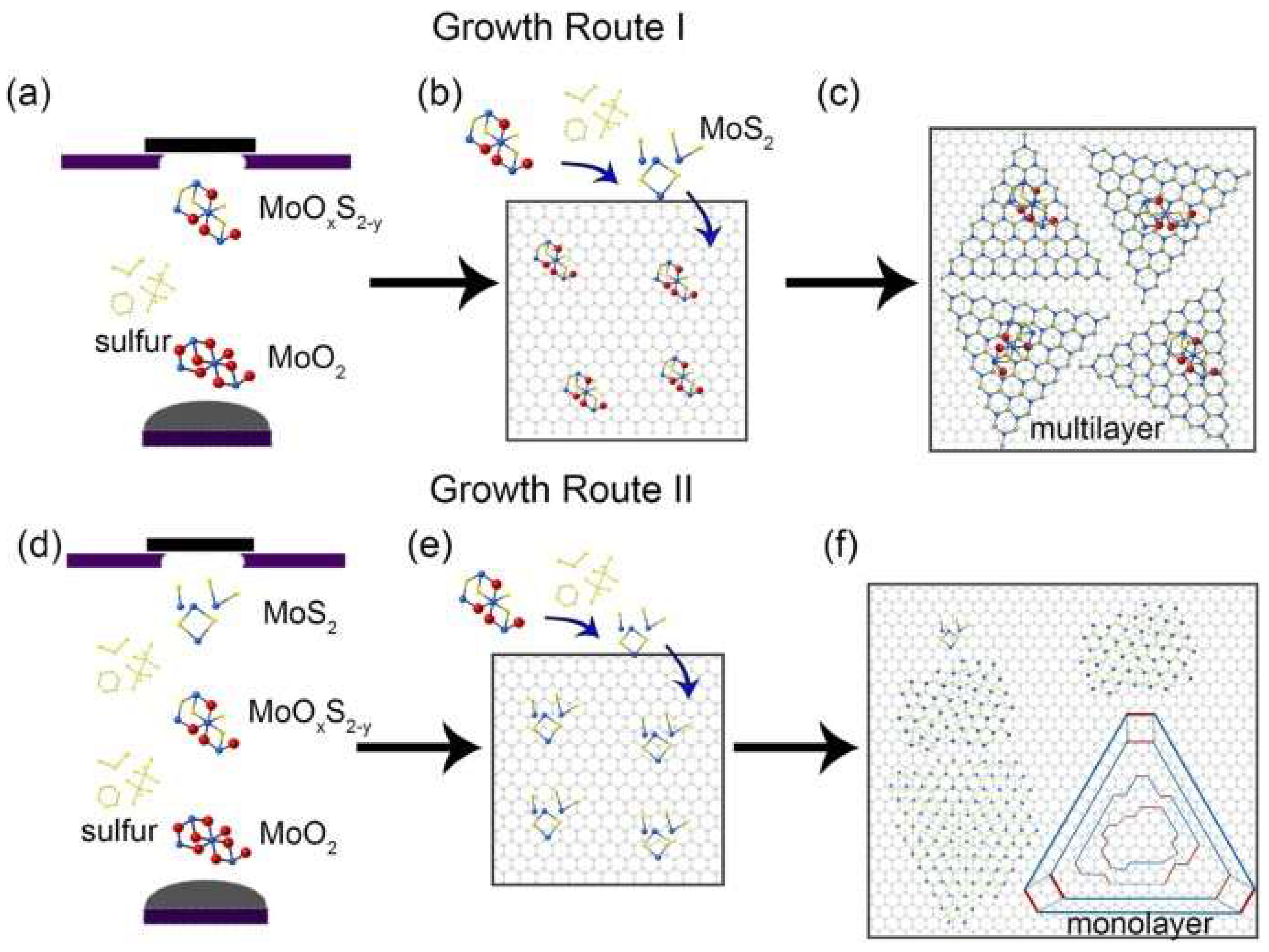
5.2. Chemical Vapor Deposition Growth Kinetics

Two-dimensional transition metal disulfide compounds (TMDs) have inspired modern technology with their unique and tunable electronic, optical, and chemical properties [137]. Therefore, it is important to study the control parameters of material preparation to obtain high-quality modern electronic films, since the performance of TMDs-based devices depends strongly on their number of layers, grain size, orientation, and morphology. Zhu et al. captured the growth mechanism of MoS2 and demonstrated agreement with the results of density functional theory calculations [138]. Figure 8a–c are schematic summaries of the microscopic processes of oligolayer MoS2 growth at low gas flow (200 sccm), and Figure 8d–f are schematic routes of MoS2 monolayer nucleation and growth kinetics. The growing MoS2 monolayer, under molybdenum-rich conditions, originates as an irregular polygonal cluster decorated with S-Mo and Mo-zz edges in a comparable ratio, forming a triangular shape with dominant Mo-zz edges as its size increases. An in-depth understanding of the CVD growth mechanisms of atomically thin MoS2 materials, as well as other related two-dimensional TMDs, will pave the way for precise control of specific functional and performance-oriented growth. Lu et al. delved into the mechanism of phase and shape evolution during MoTe2 growth [139], where low growth temperature and low Te concentration can induce small growth strain potentials leading to triangular and hexagonal 2H MoTe2 growth. Whereas higher growth temperatures and higher Te concentrations can induce larger strain potentials, which are favorable for the preparation of long, irregular 1T’ MoTe2, this exploration is an important guide for the controllable preparation of phases and shapes of other 2D materials.
Conformal control is also important for the scalable synthesis of high-quality TMDs, which further ensures high-quality and high-performance applications in terms of optoelectronic and electronic properties. Single-layer TMDs with different morphologies such as triangular, star, pentagonal, hexagonal, etc. have been synthesized by CVD [140]. Many studies have shown that the morphology of the TMDs layer is related to the growth conditions, including substrate, gas flow rate, temperature, precursor ratio, and concentration. For example, it has been found that hydrogen gas has a great influence on the morphology of TMDs during the growth process, and the shape of the monolayer triangular WS2 can be adjusted from a sawtooth shape to a straight edge shape by adding a small amount of H2 gas [141]. Similarly, with the increase of H2 concentration, more WO3 is reduced by H2 to volatile WO3−x by depositing W atoms at the Se edge, while appropriate fluxes of WO3−x and Se can be formed into W/Se-edge triangles or hexagonal shapes with high selectivity by controlling the H2 pressure [142]. In addition, the distance between the metal source and the substrate determines the concentration of the vapor metal precursor, which plays a crucial role in the morphological control of MoS2 [143]. With increasing distance from the MoO3 precursor, MoS2 transforms from medium-sized truncated triangles of ~6 μm to large triangles of ~50 μm and then increases to medium-sized truncated triangles, then small hexagons, and finally small triangles of ~2–3 μm. The parameters of this shape evolution strongly depend on the growth rates of the different edge ends.
When the Mo: S ratio is 1:2, the growth rates of the different side ends are equal, forming hexagons. When the Mo: S ratio is greater than 1:2, the zigzag (zz) end of S grows faster than the Mo-zz end due to the higher probability of the exposed S atoms combining with the free Mo atoms, so the final structure shifts to a triangle with Mo-zz end edges [144]. On the contrary, when the substrate is farther away from the Mo source, the Mo vapor concentration decreases while the S vapor gradient is smaller, then the Mo: S ratio is less than 1:2, and the S-zz triangle is obtained. It has also been suggested that the edges of Mo-zz triangles are sharper and straighter than those of S-zz triangles, which allows optical microscopy to recognize the orientation of the crystals [145].

6. Machine Learning Enables Growth Modulation of 2D Materials

6.1. Monitoring the Growth Process

Given the vast amount of experimental data, simulation results, and the accessibility of large materials databases, machine learning techniques have become more prevalent in materials science research applications [136,146]. These data resources provide a solid foundation for training statistical models, and in the field of chemical vapor deposition growth, machine learning has demonstrated a wide range of potential applications by being able to accurately predict the type of growth that may occur based on specific process conditions. Wang et al. constructed an ML Gaussian regression model to explore the growth mechanism of MoS2 materials prepared by the CVD method using machine learning to assist the large-area preparation of molybdenum disulfide materials [20]. The parameters of the regression model were evaluated by combining the index metrics of goodness-of-fit (r2), mean square error (MSE), and Pearson correlation coefficient (p). The optimal model was used to predict the synthesis particle size of molybdenum disulfide under 185,900 experimental conditions in the simulated dataset, to select the optimal range for the synthesis of large-sized molybdenum disulfide. Lu et al. utilized four machine learning algorithms [21], XGBoost, SVM, NB, and Multi-Layer Perceptron (MLP), to construct a prediction model to explore the growth mechanism of MoS2 material layers prepared by the CVD method. In addition, the models were evaluated using performance assessment metrics such as recall, specificity, accuracy, and ROC curve. Using 50% of the predicted results as a cut-off, the results were predicted and the range of each growth condition was circled using virtual data. Optimization of growth conditions by machine learning algorithms is expected to enhance control over the preparation of molybdenum disulfide layers, thereby facilitating the development of electronic and optoelectronic devices.
Krishnamoorthy et al. used a feed-forward neural network with three hidden layers to identify the different phases present during the computational synthesis of MoSe2 [147]. The goal is to perform tens of billions of quantum mechanical simulations using multi-million atom quantum dynamics simulations from the neural network and deep learning using small QMD simulations. Research on extracting optimal growth conditions from machine learning models has also been carried out. A crowdsourced database of synthesis routes and experimental results of graphene CVD growth has been developed by Schiller et al. Many parameters, including catalyst composition [148], ambient temperature, reactor specifications, spectroscopy, and microscopy results, are included in the database and processed by ML algorithms to predict actual synthesis routes. The database has the potential to accelerate the discovery of CVD routes for 2D material synthesis. Costine et al. developed an ML-based method to predict MoS2 growth, utilizing data from published growth experiments to predict growth properties in unexplored regions of parameter space. A database of MoS2 films was manually constructed from literature data on the growth of MoS2 films by chemical vapor deposition. Unsupervised multidimensional scaling (MDS) analyses were performed using growth variables such as Mo and S precursor temperatures, maximum growth temperature, growth time, and pressure. The significance of each feature was extracted from a random forest model, indicating that the Mo precursor temperature had the most significant effect on the growth process. Design rules for establishing phase boundaries that distinguish monolayers from other possible outcomes are revealed, guiding future CVD experiments [149].
Xu et al. used a trained ML model to optimize the growth parameters [150]. This work implements supervised ML on the CVD synthesis of a few-layered 1T’ WTe2, and the paradigm is schematically depicted in Figure 9. From the feature importance study, it was concluded that hydrogen flow rate and reaction temperature are the most critical parameters. It was observed that augmenting the experimental results with machine learning models can accelerate the development of nanoribbons. Tang et al. extended the application of machine learning to guide the material synthesis process through the establishment of model building [151], optimization, and progressive adaptive modeling (PAM). Two representative multivariate systems were studied. A classified ML model for the chemical vapor phase growth of molybdenum disulfide was established to optimize the synthesis conditions and improve the synthesis success rate. A regression model for the hydrothermal growth of carbon quantum dots was established to improve its process-related properties such as photoluminescence quantum yield. The importance of the synthesis parameters for the experimental results was extracted especially from the constructed ML model. Offline analyses show that the use of an effective feedback loop in PAM can enhance experimental results with a minimum number of trials, suggesting great potential for introducing ML to guide the synthesis of new materials at the beginning stages. PAM is used to enhance the results of experimental synthesis processes. The authors used a dataset containing the results of 300 experiments in which 183 growths were successfully observed, and a binary classification problem was naturally formed from the available data. Seven features with a complete dataset were considered in the feature importance study, including gas flow rate, reaction temperature and time, ramp time, distance to the sulfur precursor outside the furnace, and ship orientation. The mutual information between the features was quantified using Pearson’s coefficient. This work provides proof-of-concept for the use of ML to facilitate the synthesis of inorganic materials, thus revealing a new and promising window into the feasibility and remarkable ability of ML to accelerate materials development.
Machine learning-driven predictions are more convenient and faster than traditional computation, and can be effective in quickly obtaining the required information from large amounts of data. These studies are geared towards modeling, predicting, and understanding the growth of CVD to gain insights that can be utilized to guide experiments.

6.2. Predicting Growth Patterns

Traditional CVD process optimization relies on empirical trial and error and physical models, which are time-consuming and costly. With the development of machine learning techniques, researchers can utilize historical experimental data and simulation results to train statistical models that can predict CVD growth patterns. These models can predict material growth patterns based on input process parameters, thus guiding process optimization.
By analyzing a large amount of experimental data, the machine learning model can identify the key process parameters that have the greatest impact on the growth pattern and recommend the optimal process conditions. Moreover, based on historical data and physical models, the machine learning algorithm can predict the growth morphology of the material under different process conditions, reducing the number of experimental trials and errors. Zhang et al. emphasized the need for data-based approaches [152], including a combination of experimentation and modeling, to overcome the challenges of achieving controlled CVD growth of 2D materials. The authors elucidate how morphology maps can facilitate the validation of hypothesized synthetic mechanisms based on available data. Indeed, by invoking data analysis and ML methods, a wealth of data on various synthetic conditions and their respective growth outcomes can lead to an unbiased assessment of synthetic routes. Material databases and models can be used to create morphological maps that can be used to guide experiments, conveniently helping to reveal potential relationships between growth results and process parameters.
Experimental data can be added to the materials database to further optimize the ML model. However, in much of the existing work, 2D crystal shapes are mapped onto CVD process variables, as shown in Figure 10a, with implications that are dependent on individual devices and difficult to generalize. For the shape maps to be universally applicable, they need to be constructed in the space of intrinsic growth parameters associated with the CVD process. As shown in Figure 10b, these parameters include thermodynamic variables such as the partial pressure of the precursor and the reaction temperature. In Figure 10c, the correlation between growth conditions and molybdenum disulfide morphology is visualized utilizing an extensive survey of what has been published on the CVD growth of two-dimensional molybdenum disulfide. Since the limited information on the growth environment provided in the literature prevents us from identifying all relevant growth parameters, the MoS2 shape is plotted in a reduced 2D space spanned by the growth temperature and partial pressure ratio of the Mo and S precursors. However, a general trend in the variation of MoS2 morphology with growth conditions can be readily recognized: as the temperature or Mo/S precursor ratio increases, the densification of MoS2 increases, and the concavity decreases. We expect a clearer picture of regions with different growth morphologies in a more comprehensive growth parameter space where the partial pressures of Mo and S precursors vary independently. In the future, the adoption of the MGI approach, which emphasizes the close integration of experimentation and modeling, with data acquisition, synthesis, and analysis as the key components, will greatly facilitate the controlled CVD growth of 2D materials (Figure 10d).
There are relatively few studies on CVD growth pattern prediction, but the application of machine learning in this field is promising. With the continuous accumulation of data resources and the advancement of algorithmic technology, integrating multi-source data, the machine learning model can more accurately predict growth morphology under different process conditions, providing a scientific basis for process optimization. The hybrid model with high interpretability and generalization ability can be developed by combining the physically driven model and deep learning technology, which can better reveal the complex mechanisms in the CVD growth process.
Automated experimental platforms and real-time monitoring technologies are rapidly developing, machine learning technologies will realize dynamic regulation of the CVD growth process and improve the efficiency and consistency of material preparation. Interdisciplinary cooperation and data sharing will promote the establishment of a standardized database, further accelerating the application and innovation of machine learning in CVD. Machine learning is expected to become a core tool for CVD growth regulation, bringing breakthroughs in materials science research and industrial production.

7. Conclusions and Outlook

Although two-dimensional materials show great potential for development in many fields, there is still a long way to go from the laboratory to practical applications. Problems such as large-area preparation, delamination shedding, defects, and detection of two-dimensional single-crystal films are still bottlenecks that limit the application of two-dimensional materials. In the past decade, the optical properties of 2D materials have been extensively explored by various optical techniques, and representative methods include optical imaging, Raman spectroscopy, PL spectroscopy, nonlinear spectroscopy, and so on. These optical techniques have certain drawbacks and limitations for studying the optical properties of 2D materials. The introduction of the ML algorithm effectively improves the accuracy, reliability, and repeatability of 2D material identification. Meanwhile, the ML algorithm provides the possibility of combining two or more optical techniques to detect the optical properties of 2D materials, which will effectively reduce the ambiguities that may result from using a single technique [153].
Many other issues must be addressed in the face of large-scale production, processing, and application of 2D materials. In the preparation of TMD materials, experimental conditions have a critical impact on their growth quality and even growth shape. However, there is still a large gap in practical applications due to differences in calculation methods, testing instruments, and data location choices. Establishing uniform, fast, inexpensive, and non-destructive measurement methods, and testing standards from the data is key to driving the implementation of industrial applications.
At present, how to solve the contradiction between accurate recognition and fuzzy features is still a difficult problem. Due to disturbing factors such as noise and environment, the images and spectra obtained during the imaging process will be distorted or interfered with. It is difficult to find a stable and reliable reference standard for optical characteristics and growth patterns because the testing conditions of the detection system are susceptible to interference and there are some differences in the equipment of different laboratories. Although optical microscopy and Raman spectroscopy have been widely used to determine the labels of training set samples, it is difficult to meet the future needs of high-speed detection. Image processing and analysis techniques are a core part of ML recognition, and it is especially important to construct a good algorithm suitable for applications in related fields. The effective use of data should be continuously evaluated to determine the most effective algorithm and to assess the accuracy of the technique. While excellent algorithms continue to emerge, they are mainly based on existing algorithmic models and lack targeted improvement and optimization, resulting in a certain gap between accuracy and meeting the needs of practical applications. Due to the large amount of data, redundant information, and high dimensionality of feature space, some algorithms have insufficient ability to extract useful information, low real-time performance, and sometimes it is difficult to fully meet the high-throughput requirements of industrial processes.
The main problem with ML applications in the materials domain is the large amount of data required, and selecting the right model to ensure speed, fit, and accurate prediction is difficult. Therefore, the effective use of data should be continuously evaluated to determine the most efficient algorithms and to assess the accuracy of the techniques. In addition, there is a need to learn complex decision boundaries that are difficult to overcome with other methods. The ML algorithm predicts expected trends based on historical data, compensates for noise, simplifies the acquisition process, and effectively reduces external interference during signal acquisition. The expectation is to maintain the atomic-scale structural integrity and surface cleanliness of sensitive 2D materials without damage during the measurement process.
In conclusion, machine learning and data-supported approaches represent the emergence of a new paradigm in materials science, which will bring about profound changes in the traditional research methods and discovery approaches for 2D materials. Table 1 highlights the types, properties, and synthesis methods of 2D nanomaterials, and their applications in ML. Machine learning is helping to accelerate the field of research and soon expand the practical applications of 2D materials [16,31,153,154,155,156,157,158,159].

Author Contributions

Conceptualization, Z.H. (Zihan Hu) and X.Q.; methodology, Z.H. (Zihan Hu); software, J.L. and X.L.; validation, Z.H. (Zihan Hu) and J.L.; formal analysis, Z.H. (Zihan Hu) investigation, Z.H. (Zihan Hu); resources, Z.H. (Zihan Hu), X.Q. and Z.H. (Zongyu Huang); data curation, Z.H. (Zihan Hu); writing—original draft preparation, Z.H. (Zihan Hu); writing—review and editing, Z.H. (Zihan Hu), X.Q., Z.H. (Zongyu Huang) and W.D.; visualization, Z.H. (Zihan Hu); supervision, X.Q., Z.H. (Zongyu Huang), W.D.; project administration, X.Q.; funding acquisition, X.Q. All authors have read and agreed to the published version of the manuscript.

Funding

This research was supported by the Natural Science Fund for Distinguished Young Scholars of Hunan Province (No. 2023JJ10037).

Data Availability Statement

No new data were created or analyzed in this study. Data sharing is not applicable to this article.

Conflicts of Interest

All authors declared that there are no conflicts of interest.

References

  1. Yu, J.; Kuang, X.; Gao, Y.; Wang, Y.; Chen, K.; Ding, Z.; Liu, J.; Cong, C.; He, J.; Liu, Z.; et al. Direct Observation of the Linear Dichroism Transition in Two-Dimensional Palladium Diselenide. Nano Lett. 2020, 20, 1172–1182. [Google Scholar] [CrossRef]
  2. Lin, Z.; Tian, Z.; Cen, W.; Zeng, Q. Monolayer black phosphorus: Tunable band gap and optical properties. Phys. B Condens. Matter 2023, 657, 414780. [Google Scholar] [CrossRef]
  3. Shi, Z.; Ren, X.; Qiao, H.; Cao, R.; Zhang, Y.; Qi, X.; Zhang, H. Recent insights into the robustness of two-dimensional black phosphorous in optoelectronic applications. J.Photochem. Photobiol. C Photochem. Rev. 2020, 43, 100354. [Google Scholar] [CrossRef]
  4. Pogorielov, M.; Smyrnova, K.; Kyrylenko, S.; Gogotsi, O.; Zahorodna, V.; Pogrebnjak, A. MXenes—A New Class of Two-Dimensional Materials: Structure, Properties and Potential Applications. Nanomaterials 2021, 11, 3412. [Google Scholar] [CrossRef]
  5. Talipova, A.B.; Buranych, V.V.; Savitskaya, I.S.; Bondar, O.V.; Turlybekuly, A.; Pogrebnjak, A.D. Synthesis, Properties, and Applications of Nanocomposite Materials Based on Bacterial Cellulose and MXene. Polymers 2023, 15, 4067. [Google Scholar] [CrossRef] [PubMed]
  6. Alagarsamy, K.N.; Saleth, L.R.; Sekaran, S.; Fusco, L.; Delogu, L.G.; Pogorielov, M.; Yilmazer, A.; Dhingra, S. MXenes as emerging materials to repair electroactive tissues and organs. Bioact. Mater. 2025, 48, 583–608. [Google Scholar] [CrossRef] [PubMed]
  7. Rafique, M.; Anwar, S.; Irshad, M.; Rafique, M.S.; Assiri, M.A. Materials design to novel properties of MXenes: A comprehensive review on compositions, structures, characteristics, synthesis strategies and electrochemical properties. J. Energy Storage 2025, 121, 116470. [Google Scholar] [CrossRef]
  8. Wang, S.; Xia, J.; Yang, X.; Xie, Q.; Zhuang, Z.; Feng, H.; Xiang, H.; Chen, Z.; Li, H.; Zhang, L.; et al. Two-dimensional materials for NOx reduction to ammonia: From electrocatalyst to system. Coord. Chem. Rev. 2025, 535, 216610. [Google Scholar] [CrossRef]
  9. Lutomia, D.; Poria, R.; Kala, D.; Garg, P.; Nagraik, R.; Kaushal, A.; Gupta, S.; Kumar, D. 2D nanomaterials in biosensing: Synthesis, characterization, integration in biosensors and their applications. Biosens. Bioelectron. X 2025, 24, 100615. [Google Scholar] [CrossRef]
  10. Butler, K.T.; Davies, D.W.; Cartwright, H.; Isayev, O.; Walsh, A. Machine learning for molecular and materials science. Nature 2018, 559, 547–555. [Google Scholar] [CrossRef]
  11. Zhang, L.; He, M.; Shao, S. Machine learning for halide perovskite materials. Nano Energy 2020, 78, 105380. [Google Scholar] [CrossRef]
  12. Frey, N.C.; Akinwande, D.; Jariwala, D.; Shenoy, V.B. Machine Learning-Enabled Design of Point Defects in 2D Materials for Quantum and Neuromorphic Information Processing. ACS Nano 2020, 14, 13406–13417. [Google Scholar] [CrossRef]
  13. Schleder, G.R.; Focassio, B.; Fazzio, A. Machine learning for materials discovery: Two-dimensional topological insulators. Appl. Phys. Rev. 2021, 8, 031409. [Google Scholar] [CrossRef]
  14. Damewood, J.; Karaguesian, J.; Lunger, J.R.; Tan, A.R.; Xie, M.; Peng, J.; Gómez-Bombarelli, R. Representations of Materials for Machine Learning. Annu. Rev. Mater. Res. 2023, 53, 399–426. [Google Scholar] [CrossRef]
  15. Acosta, C.M.; Ogoshi, E.; Souza, J.A.; Dalpian, G.M. Machine Learning Study of the Magnetic Ordering in 2D Materials. ACS Appl. Mater. Interfaces 2022, 14, 9418–9432. [Google Scholar] [CrossRef]
  16. Zhong, X.; Gallagher, B.; Liu, S.; Kailkhura, B.; Hiszpanski, A.; Han, T.Y.-J. Explainable machine learning in materials science. npj Comput. Mater. 2022, 8, 204. [Google Scholar] [CrossRef]
  17. Schleder, G.R.; Acosta, C.M.; Fazzio, A. Exploring Two-Dimensional Materials Thermodynamic Stability via Machine Learning. ACS Appl. Mater. Interfaces 2020, 12, 20149–20157. [Google Scholar] [CrossRef]
  18. Li, Y.; Kong, Y.; Peng, J.; Yu, C.; Li, Z.; Li, P.; Liu, Y.; Gao, C.-F.; Wu, R. Rapid identification of two-dimensional materials via machine learning assisted optic microscopy. J. Mater. 2019, 5, 413–421. [Google Scholar] [CrossRef]
  19. Hu, X.; Qiu, C.; Liu, D. Rapid thin-layer WS2 detection based on monochromatic illumination photographs. Nano Res. 2021, 14, 840–845. [Google Scholar] [CrossRef]
  20. Wang, J.; Lu, M.; Chen, Y.; Hao, G.; Liu, B.; Tang, P.; Yu, L.; Wen, L.; Ji, H. Machine Learning-Assisted Large-Area Preparation of MoS2 Mater. Nanomaterials 2023, 13, 2283. [Google Scholar] [CrossRef]
  21. Lu, M.; Ji, H.; Chen, Y.; Gao, F.; Liu, B.; Long, P.; Deng, C.; Wang, Y.; Tao, J. Machine learning assisted layer-controlled synthesis of MoS2. J. Mater. Chem. C 2024, 12, 8893–8900. [Google Scholar] [CrossRef]
  22. Yin, H.; Sun, Z.; Wang, Z.; Tang, D.; Pang, C.H.; Yu, X.; Barnard, A.S.; Zhao, H.; Yin, Z. The data-intensive scientific revolution occurring where two-dimensional materials meet machine learning. Cell Rep. Phys. Sci. 2021, 2, 100482. [Google Scholar] [CrossRef]
  23. Mouzai, M.; Oukid, S.; Mustapha, A. Machine learning modeling for the prediction of materials energy. Neural Comput. Appl. 2022, 34, 17981–17998. [Google Scholar] [CrossRef]
  24. Zheng, S.; Ding, H.; Li, S.; Chen, D.; Pan, F. Application of topology-based structure features for machine learning in materials science. CJSC 2023, 42, 100120. [Google Scholar] [CrossRef]
  25. Bi, Q.; Goodman, K.E.; Kaminsky, J.; Lessler, J. What is Machine Learning? A Primer for the Epidemiologist. Am. J. Epidemiology 2019, 188, 2222–2239. [Google Scholar] [CrossRef]
  26. Mahesh, B. Machine Learning Algorithms—A Review. Int. J. Sci. Res. 2019, 9, 381–386. [Google Scholar] [CrossRef]
  27. Jordan, M.I.; Mitchell, T.M. Machine learning: Trends, perspectives, and prospects. Science 2015, 349, 255–260. [Google Scholar] [CrossRef]
  28. El Naqa, I.; Murphy, M.J. What Is Machine Learning? In Machine Learning in Radiation Oncology: Theory and Applications; El Naqa, I., Li, R., Murphy, M.J., Eds.; Springer International Publishing: Cham, Switzerland, 2015; pp. 3–11. [Google Scholar]
  29. Carleo, G.; Cirac, I.; Cranmer, K.; Daudet, L.; Schuld, M.; Tishby, N.; Vogt-Maranto, L.; Zdeborová, L. Machine learning and the physical sciences. Rev. Mod. Phys. 2019, 91, 045002. [Google Scholar] [CrossRef]
  30. Nasteski, V. An overview of the supervised machine learning methods. Horiz. B 2017, 4, 51–62. [Google Scholar] [CrossRef]
  31. Mao, Y.; Wang, L.; Chen, C.; Yang, Z.; Wang, J. Thickness Determination of Ultrathin 2D Materials Empowered by Machine Learning Algorithms. Laser Photonics Rev. 2023, 17, 2200357. [Google Scholar] [CrossRef]
  32. Haifeng, W.; Dejin, H. Comparison of SVM and LS-SVM for Regression. In Proceedings of the International Conference on Neural Networks and Brain, Beijing, China, 13–15 October 2005; pp. 279–283. [Google Scholar] [CrossRef]
  33. Chandra, M.A.; Bedi, S.S. Survey on SVM and their application in imageclassification. Int. J. Inform. Technol. 2021, 13, 1–11. [Google Scholar]
  34. Vishwanathan, S.V.M.; Murty, M.N. SSVM: A simple SVM algorithm. In Proceedings of the International Joint Conference on Neural Networks. IJCNN’02 (Cat. No.02CH37290), Honolulu, HI, USA, 12–17 May 2002; pp. 2393–2398. [Google Scholar] [CrossRef]
  35. Sha’abani, M.N.A.H.; Fuad, N.; Jamal, N.; Ismail, M.F. kNN and SVM Classification for EEG: A Review. In Proceedings of the 5th International Conference on Electrical, Control & Computer Engineering, Kuantan, Malaysia, 29 July 2019; pp. 555–565. [Google Scholar]
  36. Guo, G.; Wang, H.; Bell, D.; Bi, Y.; Greer, K. KNN Model-Based Approach in Classification. In On the Move to Meaningful Internet Systems 2003: CoopIS, DOA, and ODBASE; Springer: Berlin/Heidelberg, Germany, 2003; pp. 986–996. [Google Scholar]
  37. Zhang, S.; Li, X.; Zong, M.; Zhu, X.; Cheng, D. Learning k for kNN Classification. J ACM Trans. Intell. Syst. Technol. 2017, 8, 43. [Google Scholar] [CrossRef]
  38. Zhang, S. Challenges in KNN Classification. IEEE Trans. Knowl. Data Eng. 2022, 34, 4663–4675. [Google Scholar] [CrossRef]
  39. Zhang, S.; Li, X.; Zong, M.; Zhu, X.; Wang, R. Efficient kNN Classification with Different Numbers of Nearest Neighbors. IEEE Trans. Neural Netw. Learn. Syst. 2018, 29, 1774–1785. [Google Scholar] [CrossRef]
  40. Ji, Y.; Yu, S.; Zhang, Y. A novel Naive Bayes model: Packaged Hidden Naive Bayes. In Proceedings of the 2011 6th IEEE Joint International Information Technology and Artificial Intelligence Conference, Chongqing, China, 20–22 August 2011; Volume 2, pp. 484–487. [Google Scholar]
  41. Jiang, L.; Zhang, H.; Cai, Z. A Novel Bayes Model: Hidden Naive Bayes. IEEE Trans. Knowl. Data Eng. 2009, 21, 1361–1371. [Google Scholar] [CrossRef]
  42. Tang, B.; Kay, S.; He, H. Toward Optimal Feature Selection in Naive Bayes for Text Categorization. IEEE Trans. Knowl. Data Eng. 2016, 28, 2508–2521. [Google Scholar] [CrossRef]
  43. Frank, E.; Trigg, L.; Holmes, G.; Witten, I.H. Technical Note: Naive Bayes for Regression. Mach. Learn. 2000, 41, 5–25. [Google Scholar] [CrossRef]
  44. Kingsford, C.; Salzberg, S.L. What are decision trees? Nat. Biotechnol. 2008, 26, 1011–1013. [Google Scholar] [CrossRef]
  45. Podgorelec, V.; Kokol, P.; Stiglic, B.; Rozman, I. Decision Trees: An Overview and Their Use in Medicine. J. Med. Syst. 2002, 26, 445–463. [Google Scholar] [CrossRef]
  46. Kotsiantis, S.B. Decision trees: A recent overview. Artif. Intell. Rev. 2013, 39, 261–283. [Google Scholar] [CrossRef]
  47. Quinlan, J.R. Induction of decision trees. Mach. Learn. 1986, 1, 81–106. [Google Scholar] [CrossRef]
  48. Quinlan, J.R. Simplifying decision trees. Int. J.Man-Mach. Stud. 1987, 27, 221–234. [Google Scholar] [CrossRef]
  49. Breiman, L. Random Forests. Mach. Learn. 2001, 45, 5–32. [Google Scholar] [CrossRef]
  50. Biau, G. Analysis of a random forests model. J. Mach. Learn. Res. 2012, 13, 1063–1095. [Google Scholar]
  51. Fawagreh, K.; Medhat, G.M.; and Elyan, E. Random forests: From early developments to recent advancements. Syst. Sci. Control Eng. 2014, 2, 602–609. [Google Scholar] [CrossRef]
  52. Cutler, D.R.; Edwards, T.C., Jr.; Beard, K.H.; Cutler, A.; Hess, K.T.; Gibson, J.; Lawler, J.J. Random Forcasts for Classification in Ecology. Ecology 2007, 88, 2783–2792. [Google Scholar] [CrossRef]
  53. Li, Z.; Liu, F.; Yang, W.; Peng, S.; Zhou, J. A Survey of Convolutional Neural Networks: Analysis, Applications, and Prospects. IEEE Trans. Neural Netw. Learn. Syst. 2022, 33, 6999–7019. [Google Scholar] [CrossRef]
  54. Gu, J.; Wang, Z.; Kuen, J.; Ma, L.; Shahroudy, A.; Shuai, B.; Liu, T.; Wang, X.; Wang, G.; Cai, J.; et al. Recent advances in convolutional neural networks. Pattern Recognit. 2018, 77, 354–377. [Google Scholar] [CrossRef]
  55. Yamashita, R.; Nishio, M.; Do, R.K.G.; Togashi, K. Convolutional neural networks: An overview and application in radiology. Insights Imaging 2018, 9, 611–629. [Google Scholar] [CrossRef]
  56. Ajit, A.; Acharya, K.; Samanta, A. A Review of Convolutional Neural Networks. In Proceedings of the International Conference on Emerging Trends in Information Technology and Engineering (ic-ETITE), Vellore, India, 24–25 February 2020; pp. 1–5. [Google Scholar]
  57. Ketkar, N.; Moolayil, J. Convolutional Neural Networks. In Deep Learning with Python: Learn Best Practices of Deep Learning Models with PyTorch; Ketkar, N., Moolayil, J., Eds.; Apress: Berkeley, CA, USA, 2021; pp. 197–242. [Google Scholar]
  58. Vedaldi, A.; Lenc, K. MatConvNet: Convolutional Neural Networks for MATLAB. In Proceedings of the 23rd ACM International Conference on Multimedia, Association for Computing Machinery, Brisban, Australia, 26–30 October 2015; pp. 689–692. [Google Scholar]
  59. Liu, Y.; Kelley, K.P.; Vasudevan, R.K.; Funakubo, H.; Ziatdinov, M.A.; Kalinin, S.V. Experimental discovery of structure–property relationships in ferroelectric materials via active learning. Nat. Mach. Intell. 2022, 4, 341–350. [Google Scholar] [CrossRef]
  60. Zhang, F.; Tamura, R.; Zeng, F.; Kozawa, D.; Kitaura, R. Bayesian Optimization for Controlled Chemical Vapor Deposition Growth of WS2. ACS Appl. Mater. Interfaces 2024, 16, 59109–59115. [Google Scholar] [CrossRef]
  61. Harris, S.B.; Vasudevan, R.; Liu, Y. Active oversight and quality control in standard Bayesian optimization for autonomous experiments. npj Comput. Mater. 2025, 11, 23. [Google Scholar] [CrossRef]
  62. van Engelen, J.E.; Hoos, H.H. A survey on semi-supervised learning. Mach. Learn. 2020, 109, 373–440. [Google Scholar] [CrossRef]
  63. Zhou, Z.-H. Semi-Supervised Learning. In Machine Learning; Springer Singapore: Singapore, 2021; pp. 315–341. [Google Scholar]
  64. Yang, X.; Song, Z.; King, I.; Xu, Z. A Survey on Deep Semi-Supervised Learning. IEEE Trans. Knowl. Data Eng. 2023, 35, 8934–8954. [Google Scholar] [CrossRef]
  65. Mallapragada, P.K.; Jin, R.; Jain, A.K.; Liu, Y. SemiBoost: Boosting for Semi-Supervised Learning. TPAMI 2009, 31, 2000–2014. [Google Scholar] [CrossRef]
  66. Johnson, J.D.; Li, J.; Chen, Z. Reinforcement Learning: An Introduction: R.S., Sutton, A.G., Barto, MIT Press, Cambridge, MA 1998, 322 pp. ISBN 0-262-19398-1. Neurocomputing 2000, 35, 205–206. [Google Scholar] [CrossRef]
  67. François-Lavet, V.; Henderson, P.; Islam, R.; Bellemare, M.G.; Pineau, J. An Introduction to Deep Reinforcement Learning. Found. Trends Mach. Learn. 2018, 11, 219–354. [Google Scholar] [CrossRef]
  68. Thrun, S.; Littman, M.L. Reinforcement Learning: An Introduction. AI Mag. 2000, 21, 103. [Google Scholar] [CrossRef]
  69. Eng, J. Receiver Operating Characteristic Analysis: A Primer1. Acad. Radiol. 2005, 12, 909–916. [Google Scholar] [CrossRef]
  70. Zweig, M.H.; Campbell, G. Receiver-operating characteristic (ROC) plots: A fundamental evaluation tool in clinical medicine. Clin. Chem. 1993, 39, 561–577. [Google Scholar] [CrossRef]
  71. Bewick, V.; Cheek, L.; Ball, J. Statistics review 13: Receiver operating characteristic curves. Crit. Care 2004, 8, 508. [Google Scholar] [CrossRef]
  72. Altman, D.G.; Bland, J.M. Diagnostic tests 3: Receiver operating characteristic plots. BMJ 1994, 309, 188. [Google Scholar] [CrossRef]
  73. Akobeng, A.K. Understanding diagnostic tests 3: Receiver operating characteristic curves. Acta Paediatr. 2007, 96, 644–647. [Google Scholar] [CrossRef] [PubMed]
  74. Nahm, F.S. Receiver operating characteristic curve: Overview and practical use for clinicians. kja 2022, 75, 25–36. [Google Scholar] [CrossRef] [PubMed]
  75. Turner, J.R. Area Under the Curve (AUC). In Encyclopedia of Behavioral Medicine; Gellman, M.D., Ed.; Springer International Publishing: Cham, Switzerland, 2020; p. 146. [Google Scholar]
  76. Purves, R.D. Optimum numerical integration methods for estimation of area-under-the-curve (AUC) and area-under-the-moment-curve (AUMC). J. Pharmacokinet. Biopharm. 1992, 20, 211–226. [Google Scholar] [CrossRef] [PubMed]
  77. Köksoy, O. Multiresponse robust design: Mean square error (MSE) criterion. Appl. Math. Comput. 2006, 175, 1716–1729. [Google Scholar] [CrossRef]
  78. Shen, H.; Li, B.; Tao, M.; Wang, X. MSE-Based Transceiver Designs for the MIMO Interference Channel. IEEE Trans. Wirel. Commun. 2010, 9, 3480–3489. [Google Scholar] [CrossRef]
  79. Jorswieck, E.A.; Boche, H. Transmission strategies for the MIMO MAC with MMSE receiver: Average MSE optimization and achievable individual MSE region. TSP 2003, 51, 2872–2881. [Google Scholar] [CrossRef]
  80. Thompson, P.A. An MSE statistic for comparing forecast accuracy across series. Int. J. Forecast. 1990, 6, 219–227. [Google Scholar] [CrossRef]
  81. Marmolin, H. Subjective MSE Measures. ITSMCS 1986, 16, 486–489. [Google Scholar] [CrossRef]
  82. Zhang, G.; Huang, S.; Wang, F.; Yan, H. Layer-Dependent Electronic and Optical Properties of 2D Black Phosphorus: Fundamentals and Engineering. Laser Photon. Rev. 2021, 15, 2000399. [Google Scholar] [CrossRef]
  83. Chen, Z.-Y.; Qin, R. Strong-field nonlinear optical properties of monolayer black phosphorus. Nanoscale 2019, 11, 16377–16383. [Google Scholar] [CrossRef]
  84. Xia, F.; Wang, H.; Jia, Y. Rediscovering black phosphorus as an anisotropic layered material for optoelectronics and electronics. Nat. Commun. 2014, 5, 4458. [Google Scholar] [CrossRef]
  85. Wang, X.; Lan, S. Optical properties of black phosphorus. Adv. Opt. Photon. 2016, 8, 618–655. [Google Scholar] [CrossRef]
  86. Huang, H.; Jiang, B.; Zou, X.; Zhao, X.; Liao, L. Black phosphorus electronics. Sci. Bull. 2019, 64, 1067–1079. [Google Scholar] [CrossRef] [PubMed]
  87. Huang, S.; Ling, X. Black Phosphorus: Optical Characterization, Properties and Applications. Small 2017, 13, 1700823. [Google Scholar] [CrossRef] [PubMed]
  88. Xin, W.; Jiang, H.B.; Sun, T.Q.; Gao, X.G.; Chen, S.N.; Zhao, B.; Yang, J.J.; Liu, Z.B.; Tian, J.G.; Guo, C.L. Optical anisotropy of black phosphorus by total internal reflection. Nano Mater. Sci. 2019, 1, 304–309. [Google Scholar] [CrossRef]
  89. Shen, W.; Sun, Z.; Huo, S.; Hu, C. Directly Evaluating the Optical Anisotropy of Few-Layered Black Phosphorus during Ambient Oxidization. Adv. Opt. Mater. 2022, 10, 2102018. [Google Scholar] [CrossRef]
  90. Jiang, H.; Shi, H.; Sun, X.; Gao, B. Optical Anisotropy of Few-Layer Black Phosphorus Visualized by Scanning Polarization Modulation Microscopy. ACS Photonics 2018, 5, 2509–2515. [Google Scholar] [CrossRef]
  91. Shen, W.; Hu, C.; Tao, J.; Liu, J.; Fan, S.; Wei, Y.; An, C.; Chen, J.; Wu, S.; Li, Y.; et al. Resolving the optical anisotropy of low-symmetry 2D materials. Nanoscale 2018, 10, 8329–8337. [Google Scholar] [CrossRef]
  92. Ogilvie, S.P.; Large, M.J.; Fratta, G.; Meloni, M.; Canton-Vitoria, R.; Tagmatarchis, N.; Massuyeau, F.; Ewels, C.P.; King, A.A.K.; Dalton, A.B. Considerations for spectroscopy of liquid-exfoliated 2D materials: Emerging photoluminescence of N-methyl-2-pyrrolidone. Sci. Rep. 2017, 7, 16706. [Google Scholar] [CrossRef] [PubMed]
  93. Tebbe, D.; Schütte, M.; Kundu, B.; Beschoten, B.; Sahoo, P.K.; Waldecker, L. Hyperspectral photoluminescence and reflectance microscopy of 2D materials. Meas. Sci. Technol. 2024, 35, 035501. [Google Scholar] [CrossRef]
  94. Kaplan, D.; Gong, Y.; Mills, K.; Swaminathan, V.; Ajayan, P.M.; Shirodkar, S.; Kaxiras, E. Excitation intensity dependence of photoluminescence from monolayers of MoS2 and WS2/MoS2 heterostructures. 2D Mater. 2016, 3, 015005. [Google Scholar] [CrossRef]
  95. Wang, Q.; Wee, A.T.S. Photoluminescence upconversion of 2D materials and applications. J. Phys. Condens. Matter 2021, 33, 223001. [Google Scholar] [CrossRef] [PubMed]
  96. Biswas, S.; Tiwary, C.S.; Vinod, S.; Kole, A.K.; Chatterjee, U.; Kumbhakar, P.; Ajayan, P.M. Nonlinear Optical Properties and Temperature Dependent Photoluminescence in hBN-GO Heterostructure 2D Material. J. Phys. Chem. C 2017, 121, 8060–8069. [Google Scholar] [CrossRef]
  97. Zhang, J.; Yu, Y.; Wang, P.; Luo, C.; Wu, X.; Sun, Z.; Wang, J.; Hu, W.D.; Shen, G. Characterization of atomic defects on the photoluminescence in two-dimensional materials using transmission electron microscope. InfoMat 2019, 1, 85–97. [Google Scholar] [CrossRef]
  98. Tebyetekerwa, M.; Zhang, J.; Xu, Z.; Truong, T.N.; Yin, Z.; Lu, Y.; Ramakrishna, S.; Macdonald, D.; Nguyen, H.T. Mechanisms and Applications of Steady-State Photoluminescence Spectroscopy in Two-Dimensional Transition-Metal Dichalcogenides. ACS Nano 2020, 14, 14579–14604. [Google Scholar] [CrossRef] [PubMed]
  99. Liu, W.; Liu, M.; Liu, X.; Wang, X.; Deng, H.-X.; Lei, M.; Wei, Z.; Wei, Z. Recent Advances of 2D Materials in Nonlinear Photonics and Fiber Lasers. Adv. Opt. Mater. 2020, 8, 1901631. [Google Scholar] [CrossRef]
  100. Wang, C.; Zhang, G.; Huang, S.; Xie, Y.; Yan, H. The Optical Properties and Plasmonics of Anisotropic 2D Materials. Adv. Opt. Mater. 2020, 8, 1900996. [Google Scholar] [CrossRef]
  101. Ma, Q.; Ren, G.; Xu, K.; Ou, J.Z. Tunable Optical Properties of 2D Materials and Their Applications. Adv. Opt. Mater. 2021, 9, 2001313. [Google Scholar] [CrossRef]
  102. Yin, P.; Jiang, X.; Huang, R.; Wang, X.; Ge, Y.; Ma, C.; Zhang, H. 2D Materials for Nonlinear Photonics and Electro-Optical Applications. Adv. Mater. Interfaces 2021, 8, 2100367. [Google Scholar] [CrossRef]
  103. Shi, J.; Feng, S.; He, P.; Fu, Y.; Zhang, X. Nonlinear Optical Properties from Engineered 2D Materials. Molecules 2023, 28, 6737. [Google Scholar] [CrossRef] [PubMed]
  104. You, J.W.; Bongu, S.R.; Bao, Q.; Panoiu, N.C. Nonlinear optical properties and applications of 2D materials: Theoretical and experimental aspects. Nanophotonics 2019, 8, 63–97. [Google Scholar] [CrossRef]
  105. Xie, Z.; Zhao, T.; Yu, X.; Wang, J. Nonlinear Optical Properties of 2D Materials and their Applications. Small 2024, 20, 2311621. [Google Scholar] [CrossRef]
  106. Zhou, L.; Fu, H.; Lv, T.; Wang, C.; Gao, H.; Li, D.; Deng, L.; Xiong, W. Nonlinear Optical Characterization of 2D Materials. Nanomaterials 2020, 10, 2263. [Google Scholar] [CrossRef] [PubMed]
  107. Ahmed, S.; Jiang, X.; Wang, C.; Kalsoom, U.E.; Wang, B.; Khan, J.; Muhammad, Y.; Duan, Y.; Zhu, H.; Ren, X.; et al. An Insightful Picture of Nonlinear Photonics in 2D Materials and their Applications: Recent Advances and Future Prospects. Adv. Opt. Mater. 2021, 9, 2001671. [Google Scholar] [CrossRef]
  108. Miao, X.; Xuan, N.; Liu, Q.; Wu, W.; Liu, H.; Sun, Z.; Ji, M. Optimizing Nonlinear Optical Visibility of Two-Dimensional Materials. ACS Appl. Mater. Interfaces 2017, 9, 34448–34455. [Google Scholar] [CrossRef]
  109. Liu, H.; Li, Z.; Yu, Y.; Lin, J.; Liu, S.; Pang, F.; Wang, T. Nonlinear optical properties of anisotropic two-dimensional layered materials for ultrafast photonics. Nanophotonics 2020, 9, 1651–1673. [Google Scholar] [CrossRef]
  110. Guo, B.; Xiao, Q.L.; Wang, S.H.; Zhang, H. 2D Layered Materials: Synthesis, Nonlinear Optical Properties, and Device Applications. Laser Photon. Rev. 2019, 13, 1800327. [Google Scholar] [CrossRef]
  111. Yamashita, S. Nonlinear optics in carbon nanotube, graphene, and related 2D materials. APL Photonics 2018, 4, 034301. [Google Scholar] [CrossRef]
  112. Zaręba, J.K.; Nyk, M.; Samoć, M. Nonlinear Optical Properties of Emerging Nano- and Microcrystalline Materials. Adv. Opt. Mater. 2021, 9, 2100216. [Google Scholar] [CrossRef]
  113. Autere, A.; Jussila, H.; Dai, Y.; Wang, Y.; Lipsanen, H.; Sun, Z. Nonlinear Optics with 2D Layered Materials. Adv. Mater. 2018, 30, 1705963. [Google Scholar] [CrossRef]
  114. Jia, J.; Ban, Y.; Liu, K.; Mao, L.; Su, Y.; Lian, M.; Cao, T. Reconfigurable Full Color Display using Anisotropic Black Phosphorus. Adv. Opt. Mater. 2021, 9, 2100499. [Google Scholar] [CrossRef]
  115. Mao, N.; Tang, J.; Xie, L.; Wu, J.; Han, B.; Lin, J.; Deng, S.; Ji, W.; Xu, H.; Liu, K.; et al. Optical Anisotropy of Black Phosphorus in the Visible Regime. J. Am. Chem. Soc. 2016, 138, 300–305. [Google Scholar] [CrossRef]
  116. Joshi, P.P.; Li, R.; Spellberg, J.L.; Liang, L.; King, S.B. Nanoimaging of the Edge-Dependent Optical Polarization Anisotropy of Black Phosphorus. Nano Lett. 2022, 22, 3180–3186. [Google Scholar] [CrossRef] [PubMed]
  117. Empedocles, S.A.; Neuhauser, R.; Shimizu, K.; Bawendi, M.G. Photoluminescence from Single Semiconductor Nanostructures. Adv. Mater. 1999, 11, 1243–1256. [Google Scholar] [CrossRef]
  118. He, K.; Kumar, N.; Zhao, L.; Wang, Z.; Mak, K.F.; Zhao, H.; Shan, J. Tightly Bound Excitons in Monolayer WSe2. Phys. Rev. Lett. 2014, 113, 026803. [Google Scholar] [CrossRef]
  119. Chernikov, A.; Berkelbach, T.C.; Hill, H.M.; Rigosi, A.; Li, Y.; Aslan, B.; Reichman, D.R.; Hybertsen, M.S.; Heinz, T.F. Exciton Binding Energy and Nonhydrogenic Rydberg Series in Monolayer WS2. Phys. Rev. Lett. 2014, 113, 076802. [Google Scholar] [CrossRef]
  120. Tanaka, K.; Hachiya, K.; Zhang, W.; Matsuda, K.; Miyauchi, Y. Machine-Learning Analysis to Predict the Exciton Valley Polarization Landscape of 2D Semiconductors. ACS Nano 2019, 13, 12687–12693. [Google Scholar] [CrossRef]
  121. Pozo-Zamudio, O.D.; Schwarz, S.; Sich, M.; Akimov, I.A.; Bayer, M.; Schofield, R.C.; Chekhovich, E.A.; Robinson, B.J.; Kay, N.D.; Kolosov, O.V.; et al. Photoluminescence of two-dimensional GaTe and GaSe films. 2D Mater. 2015, 2, 035010. [Google Scholar] [CrossRef]
  122. Molas, M.R.; Macewicz, Ł.; Wieloszyńska, A.; Jakóbczyk, P.; Wysmołek, A.; Bogdanowicz, R.; Jasinski, J.B. Photoluminescence as a probe of phosphorene properties. npj 2D Mater. Appl. 2021, 5, 83. [Google Scholar] [CrossRef]
  123. Tsu, R.; Shen, H.; Dutta, M. Correlation of Raman and photoluminescence spectra of porous silicon. Appl. Phys. Lett. 1992, 60, 112–114. [Google Scholar] [CrossRef]
  124. Mortazavi, B.; Shahrokhi, M.; Shojaei, F.; Rabczuk, T.; Zhuang, X. A machine learning-assisted exploration of the structural stability, electronic, optical, heat conduction and mechanical properties of C3N4 graphitic carbon nitride monolayers. Comput. Mater. Today 2025, 5, 100024. [Google Scholar] [CrossRef]
  125. Mortazavi, B. Recent Advances in Machine Learning-Assisted Multiscale Design of Energy Materials. Adv. Energy Mater. 2025, 15, 57. [Google Scholar] [CrossRef]
  126. Dong, Y.; Wan, J.; Wang, X.; Xue, J.H.; Zou, J.; He, H.; Li, P.; Hou, A.; Ma, H. A Polarization-Imaging-Based Machine Learning Framework for Quantitative Pathological Diagnosis of Cervical Precancerous Lesions. IEEE Trans. Med. Imaging 2021, 40, 3728–3738. [Google Scholar] [CrossRef]
  127. Nolen, C.M.; Denina, G.; Teweldebrhan, D.; Bhanu, B.; Balandin, A.A. High-Throughput Large-Area Automated Identification and Quality Control of Graphene and Few-Layer Graphene Films. ACS Nano 2011, 5, 914–922. [Google Scholar] [CrossRef]
  128. Lin, X.; Si, Z.; Fu, W.; Yang, J.; Guo, S.; Cao, Y.; Zhang, J.; Wang, X.; Liu, P.; Jiang, K.; et al. Intelligent identification of two-dimensional nanostructures by machine-learning optical microscopy. Nano Res. 2018, 11, 6316–6324. [Google Scholar] [CrossRef]
  129. Solís-Fernández, P.; Ago, H. Machine Learning Determination of the Twist Angle of Bilayer Graphene by Raman Spectroscopy: Implications for van der Waals Heterostructures. ACS Appl. Nano Mater. 2022, 5, 1356–1366. [Google Scholar] [CrossRef]
  130. Yang, J.; Yao, H. Automated identification and characterization of two-dimensional materials via machine learning-based processing of optical microscope images. Extreme Mech. Lett. 2020, 39, 100771. [Google Scholar] [CrossRef]
  131. Han, B.; Lin, Y.; Yang, Y.; Mao, N.; Li, W.; Fatemi, V.; Zhou, L.; Wang, J.; Ma, Q.; Cao, Y.; et al. Deep Learning Enabled Fast Optical Characterization of Two-Dimensional Materials. Adv. Mater. 2019, 32, 2000953. [Google Scholar] [CrossRef]
  132. Hu, Z.; Chen, W.; Qiao, H.; Huang, Z.; Qi, X. Machine Learning for Optical Anisotropy Identification of Few-Layer Black Phosphorus Based on Polarized Microscopic Images. ACS Appl. Nano Mater. 2024, 7, 27418–27425. [Google Scholar] [CrossRef]
  133. Liu, H.; Zhang, T.; Wu, P.; Lee, H.W.; Liu, Z.; Tang, T.W.; Tang, S.-Y.; Kang, T.; Park, J.-H.; Wang, J.; et al. Boosting Monolayer Transition Metal Dichalcogenides Growth by Hydrogen-Free Ramping during Chemical Vapor Deposition. Nano Lett. 2024, 24, 8277–8286. [Google Scholar] [CrossRef] [PubMed]
  134. Lara Saenz, G.A.; Biswas, C.; Yamaguchi, H.; Narvaez Villarrubia, C.; Mohite, A.D.; Kaul, A.B. Effects of Synthesis Parameters on CVD Molybdenum Disulfide Growth. MRS Adv. 2016, 1, 2291–2296. [Google Scholar] [CrossRef]
  135. Zhang, Z.; Lagally, M.G. Atomistic Processes in the Early Stages of Thin-Film Growth. Science 1997, 276, 377–383. [Google Scholar] [CrossRef] [PubMed]
  136. Bhowmik, S.; Govind Rajan, A. Chemical vapor deposition of 2D materials: A review of modeling, simulation, and machine learning studies. iScience 2022, 25, 103832. [Google Scholar] [CrossRef]
  137. You, J.; Hossain, M.D.; Luo, Z. Synthesis of 2D transition metal dichalcogenides by chemical vapor deposition with controlled layer number and morphology. Nano Converg. 2018, 5, 26. [Google Scholar] [CrossRef]
  138. Zhu, D.; Shu, H.; Jiang, F.; Lv, D.; Asokan, V.; Omar, O.; Yuan, J.; Zhang, Z.; Jin, C. Capture the growth kinetics of CVD growth of two-dimensional MoS2. npj 2D Mater. Appl. 2017, 1, 8. [Google Scholar] [CrossRef]
  139. Lu, D.; Luo, C.; Qi, X.; Zhong, J. Robust temperature–strain coupling in phase and shape evolution of MoTe2 nanosheets. Appl. Phys. Lett. 2023, 122, 171902. [Google Scholar] [CrossRef]
  140. Zhang, G.; Wang, J.; Wu, Z.; Shi, R.; Ouyang, W.; Amini, A.; Chandrashekar, B.N.; Wang, N.; Cheng, C. Shape-Dependent Defect Structures of Monolayer MoS2 Crystals Grown by Chemical Vapor Deposition. ACS Appl. Mater. Interfaces 2017, 9, 763–770. [Google Scholar] [CrossRef]
  141. Zhang, Y.; Zhang, Y.; Ji, Q.; Ju, J.; Yuan, H.; Shi, J.; Gao, T.; Ma, D.; Liu, M.; Chen, Y.; et al. Controlled Growth of High-Quality Monolayer WS2 Layers on Sapphire and Imaging Its Grain Boundary. ACS Nano 2013, 7, 8963–8971. [Google Scholar] [CrossRef]
  142. Chen, J.; Liu, B.; Liu, Y.; Tang, W.; Nai, C.T.; Li, L.; Zheng, J.; Gao, L.; Zheng, Y.; Shin, H.S.; et al. Chemical Vapor Deposition of Large-Sized Hexagonal WSe2 Crystals on Dielectric Substrates. Adv. Mater. 2015, 27, 6722–6727. [Google Scholar] [CrossRef] [PubMed]
  143. Wang, S.; Rong, Y.; Fan, Y.; Pacios, M.; Bhaskaran, H.; He, K.; Warner, J.H. Shape Evolution of Monolayer MoS2 Crystals Grown by Chemical Vapor Deposition. Chem. Mater. 2014, 26, 6371–6379. [Google Scholar] [CrossRef]
  144. Govind Rajan, A.; Warner, J.H.; Blankschtein, D.; Strano, M.S. Generalized Mechanistic Model for the Chemical Vapor Deposition of 2D Transition Metal Dichalcogenide Monolayers. ACS Nano 2016, 10, 4330–4344. [Google Scholar] [CrossRef] [PubMed]
  145. van der Zande, A.M.; Huang, P.Y.; Chenet, D.A.; Berkelbach, T.C.; You, Y.; Lee, G.-H.; Heinz, T.F.; Reichman, D.R.; Muller, D.A.; Hone, J.C. Grains and grain boundaries in highly crystalline monolayer molybdenum disulphide. Nat. Mater. 2013, 12, 554–561. [Google Scholar] [CrossRef] [PubMed]
  146. Yoshihara, N.; Tahara, Y.; Noda, M. Machine learning method for determining chemical vapor deposition conditions for large-area graphene growth. Asia-Pac. J. Chem. Eng. 2023, 18, e2911. [Google Scholar] [CrossRef]
  147. Krishnamoorthy, A.; Rajak, P.; Hong, S.; Nomura, K.-i.; Tiwari, S.; Kalia, R.K.; Nakano, A.; Vashishta, P. Reactive molecular dynamics simulations and machine learning. J. Phys. Conf. Ser. 2020, 1461, 012182. [Google Scholar] [CrossRef]
  148. Schiller, J.A.; Toro, R.; Shah, A.; Surana, M.; Zhang, K.; Robertson, M.; Miller, K.; Cruse, K.; Liu, K.; Seong, B.; et al. Crowd-Sourced Data and Analysis Tools for Advancing the Chemical Vapor Deposition of Graphene: Implications for Manufacturing. ACS Appl. Nano Mater. 2020, 3, 10144–10155. [Google Scholar] [CrossRef]
  149. Costine, A.; Delsa, P.; Li, T.; Reinke, P.; Balachandran, P.V. Data-driven assessment of chemical vapor deposition grown MoS2 monolayer thin films. J. Appl. Phys. 2020, 128, 235303. [Google Scholar] [CrossRef]
  150. Xu, M.; Tang, B.; Lu, Y.; Zhu, C.; Lu, Q.; Zhu, C.; Zheng, L.; Zhang, J.; Han, N.; Fang, W.; et al. Machine Learning Driven Synthesis of Few-Layered WTe2 with Geometrical Control. J. Am. Chem. Soc. 2021, 143, 18103–18113. [Google Scholar] [CrossRef]
  151. Tang, B.; Lu, Y.; Zhou, J.; Chouhan, T.; Wang, H.; Golani, P.; Xu, M.; Xu, Q.; Guan, C.; Liu, Z. Machine learning-guided synthesis of advanced inorganic materials. Mater. Today 2020, 41, 72–80. [Google Scholar] [CrossRef]
  152. Zhang, J.; Wang, F.; Shenoy, V.B.; Tang, M.; Lou, J. Towards controlled synthesis of 2D crystals by chemical vapor deposition (CVD). Mater. Today 2020, 40, 132–139. [Google Scholar] [CrossRef]
  153. He, H.; Wang, Y.; Qi, Y.; Xu, Z.; Li, Y.; Wang, Y. From prediction to design: Recent advances in machine learning for the study of 2D materials. Nano Energy 2023, 118, 108965. [Google Scholar] [CrossRef]
  154. Das, S.; Mazumdar, H.; Khondakar, K.R.; Kaushik, A. Machine Learning Assisted Enhancement in a Two-Dimensional Material’s Sensing Performance. ACS Appl. Nano Mater. 2024, 7, 13893–13918. [Google Scholar] [CrossRef]
  155. Liu, Y.; Lin, L.; Sun, H.-B. Optical Modification of Two-Dimensional Materials: From Atomic to Electronic Scale. J. Phys. Chem. C 2024, 128, 2271–2290. [Google Scholar] [CrossRef]
  156. Wu, P.; He, T.; Zhu, H.; Wang, Y.; Li, Q.; Wang, Z.; Fu, X.; Wang, F.; Wang, P.; Shan, C.; et al. Next-generation machine vision systems incorporating two-dimensional materials: Progress and perspectives. InfoMat 2022, 4, e12275. [Google Scholar] [CrossRef]
  157. Gaultois, M.W.; Sparks, T.D.; Borg, C.K.H.; Seshadri, R.; Bonificio, W.D.; Clarke, D.R. Data-Driven Review of Thermoelectric Materials: Performance and Resource Considerations. Chem. Mater. 2013, 25, 2911–2920. [Google Scholar] [CrossRef]
  158. Das, S.; Pegu, H.; Sahu, K.K.; Nayak, A.K.; Ramakrishna, S.; Datta, D.; Swayamjyoti, S. 19—Machine learning in materials modeling—Fundamentals and the opportunities in 2D materials. In Synthesis, Modeling, and Characterization of 2D Materials, and Their Heterostructures; Yang, E.-H., Datta, D., Ding, J., Hader, G., Eds.; Elsevier: Amsterdam, The Netherlands, 2020; pp. 445–468. [Google Scholar]
  159. Wang, Z.; Yang, M.; Xie, X.; Yu, C.; Jiang, Q.; Huang, M.; Algadi, H.; Guo, Z.; Zhang, H. Applications of machine learning in perovskite materials. Adv. Compos. Hybrid Mater. 2022, 5, 2700–2720. [Google Scholar] [CrossRef]
  160. Beckham, J.L.; Wyss, K.M.; Xie, Y.C.; McHugh, E.A.; Li, J.T.; Advincula, P.A.; Chen, W.Y.; Lin, J.; Tour, J.M. Machine Learning Guided Synthesis of Flash Graphene. Adv. Mater. 2022, 34, 11. [Google Scholar] [CrossRef]
  161. Park, J.-H.; Lu, A.-Y.; Tavakoli, M.M.; Kim, N.Y.; Chiu, M.-H.; Liu, H.; Zhang, T.; Wang, Z.; Wang, J.; Martins, L.G.P.; et al. Revealing Variable Dependences in Hexagonal Boron Nitride Synthesis via Machine Learning. Nano Lett. 2023, 23, 4741–4748. [Google Scholar] [CrossRef]
  162. Rajan, A.C.; Mishra, A.; Satsangi, S.; Vaish, R.; Mizuseki, H.; Lee, K.-R.; Singh, A.K. Machine-Learning-Assisted Accurate Band Gap Predictions of Functionalized MXene. Chem. Mater. 2018, 30, 4031–4038. [Google Scholar] [CrossRef]
Figure 1. The framework of this synthesis.
Chemistry 07 00080 g001
Figure 2. Overview of ML methods. Includes four main categories: supervised learning, unsupervised learning, semi-supervised learning, and reinforcement learning. Ref. [31] with permission from Wiley, copyright 2023.
Chemistry 07 00080 g002
Figure 3. The general process of machine learning. Ref. [20] with permission from MDPI, copyright 2023.
Chemistry 07 00080 g003
Figure 4. (a) Schematic of the optical contrast calculation. Ref. [115] with permission from American Chemical Society, copyright 2016. (b) Optical contrast of the few-layer BP measured in the RGB channel as a function of rotation angle. Ref. [115] with permission from American Chemical Society, copyright 2016. (c) Schematic of NNI PEEM. Ref. [116] with permission from American Chemical Society, copyright 2022. (d) Average phase shift ⟨δβ⟩ as a function of edge orientation γ, shown schematically in the inset, for five different black phosphorus flakes (use different colors to differentiate). Ref. [116] with permission from American Chemical Society, copyright 2022.
Chemistry 07 00080 g004
Figure 5. Crystalline orientation identification using angle-dependent optical contrast. (a) Optical image of a few-layer BP on a 300 nm SiO2/Si substrate. The dashed double arrows indicate the identified AC and ZZ directions by using the angle-dependent optical contrast of this sample. (Scale bar: 50 μm) Ref. [84] with permission from Springer Nature, copyright 2014. (b) Raman spectra of the BP sample with different rotation angles (Scale bar: 50 μm, ϕ is the angle between the x direction and the 0° reference). Ref. [84] with permission from Springer Nature, copyright 2014. Polar plot of (c) A g 2 Raman band and (d) optical contrast of the few-layer BP in G channel as a function of rotation angle. Ref. [115] with permission from American Chemical Society, copyright 2016. Ref. [115] with permission from American Chemical Society, copyright 2016.
Chemistry 07 00080 g005
Figure 6. The schematic illustration of the machine learning-assisted identification. In the training process, from optical image (a) of 2D material, the RGB values and coordinates of every pixel are obtained; analyzing RGB values by K-mean clustering, 4 clusters (b) are deduced; combining corresponding AFM results (c) of the sample with the reconstructed optical image based on the clustered data, the training processes of 2D material (d) is completed. For the testing process, using the optical image (e) of 2D material and the above-produced database, the layer-identified image (f) is obtained. Ref. [18] with permission from Elsevier, copyright 2019.
Chemistry 07 00080 g006
Figure 7. Sample image processing. (a) Variation of the RGB value of the area marked by the red box of the optical image for the rotation angle. (b) Variation relationship of gray value with rotation angle for the blue box-marked region of the grayscale image. The inset shows a single-channel separated grayscale image (40 μm in scale). (c) Feature importance analysis based on RF and decision tree models. (d) Comparison of the performance of RF, SVM, KNN, and NB models (The closer to 1 means better performance). Ref. [132] with permission from American Chemical Society, copyright 2024.
Chemistry 07 00080 g007
Figure 8. (ac) Schematic sketches explaining the possible route for the nucleation and growth kinetics of few-layer MoS2 bound with a thick core, and (df) for the nucleation and growth kinetics of MoS2 monolayers. Ref. [138] with permission from Springer Nature, copyright 2017.
Chemistry 07 00080 g008
Figure 9. Design framework for the realization of geometry-controlled CVD synthesis of WTe2 based on machine learning and experiments. Five CVD parameters were identified as significant input features (x): source ratio (RTe/W, the molar ratio of tellurium power and tungsten power), reaction temperature (T, in °C), ramp time (tR, in min), deposition time (tD, in min), and H2 gas flow rate (FH2, sccm). (scale bar, 20 μm). Ref. [150] with permission from American Chemical Society, copyright 2021.
Chemistry 07 00080 g009
Figure 10. (a) Nakaya pattern sketches of monolayers of molybdenum disulfide grown in the space spanned by process variables for CVD experiments. (b) Schematic illustration of a complete morphology diagram. The intrinsic growth parameters in this case are partial pressures of Mo (PMo) and S (PS) precursors and reaction temperature (T). (c) Summary of reported CVD growth of monolayer MoS2 on SiO2/Si substrate using MoO3 and S as precursors. MoS2 prefers to form a more ‘dendritic’ shape at lower Mo/S ratio and temperature (bottom-left region) and a more ‘compact’ shape athigher Mo/S ratio and temperature (top-right region). (d) An MGI approach to establish the morphology diagrams of 2D crystals through integrated crystal growth experiments, modeling, and database development [152]. Ref. [152] with permission from Elsevier, copyright 2020.
Chemistry 07 00080 g010
Table 1. Types, properties, synthesis methods of 2D materials, and their applications in ML.
2D NanomaterialChemical CompositionPropertiesSynthesis MethodsApplications in MLReference
GrapheneC60, C60H10, C70, etc.High Conductivity, High Strength, High Thermal Conductivity, High Light TransmissionMechanical stripping, CVD growth, chemical redox methodML Analyzes Complex Nanofabrication Processes for Guided Flash Graphene SynthesisBeckham et al. [160]
(2022)
Transition Metal Dichalcogenides (TMDs)MoS2, WS2, MoSe2, WSe2, etc.Strong exciton effect, tunable electronic structure, superconductivityCVD growth, mechanical stripping, and liquid phase strippingML optimization of growth conditions and enhanced control of molybdenum disulfide layer preparationLu et al. [21]
(2024)
Boron Nitride (BN)BNInsulating, high thermal conductivity, chemically inert, atomically flatCVD growth, high temperature and high pressure synthesis, stripping methodAnalysis of growth mechanisms by machine learning reveals variable dependence in hexagonal boron nitride synthesisPark et al. [161]
(2023)
Black Phosphorus (BP)PnTunable Bandgap, High Carrier Mobility, Optical/Electrical AnisotropyMechanical Stripping, Liquid Phase StrippingML predicts optical anisotropy characteristics of BP samples by analyzing RGB valuesPark et al. [132]
(2024)
MXeneTi3C2, V2C, Nb2C, etc.High conductivity, hydrophilic surfaceHF etching MAX phase, molten salt method, liquid phase strippingML-Assisted Functionalization of MXene for Accurate Bandgap PredictionRajan et al. [162]
(2018)
Disclaimer/Publisher’s Note: The statements, opinions and data contained in all publications are solely those of the individual author(s) and contributor(s) and not of MDPI and/or the editor(s). MDPI and/or the editor(s) disclaim responsibility for any injury to people or property resulting from any ideas, methods, instructions or products referred to in the content.

