1. Introduction
The photonic spin Hall effect refers to the phenomenon that when linearly polarized light propagates in a medium with an inhomogeneous refractive index, the left-spinning and right-spinning photons separate in opposite directions under the action of the external field played by the refractive index gradient of the medium, resulting in the splitting of the beam into two beams of circularly polarized light [
1,
2]. These two beams of light are separated on both sides of the cross section perpendicular to the plane of incidence [
3], which is essentially a physical phenomenon related to the spin trajectory of the photon caused by spin–orbit interaction [
4,
5]. Usually, the PSHE is a weak effect, and the spin transverse shift is generally only a fraction of the wavelength, which is difficult to observe directly, so how to amplify and modulate it is an urgent problem at present. Current research on the amplification and modulation of the PSHE primarily focuses on constructing refractive index gradients by tailoring the material composition and structural design of transmission media. However, once the material and structure are determined, they become fixed, making dynamic control of the PSHE challenging. To address this limitation, external fields such as electric or magnetic fields have been introduced to enable flexible PSHE modulation. As another common external stimulus, thermal effects can induce temperature-dependent refractive index changes (thermo-optic effect), suggesting their potential for actively tuning and enhancing the PSHE.
A metasurface is an ultrathin two-dimensional plane consisting of a periodic arrangement of artificial electromagnetic units, the thickness of which is much less than the operating wavelength. In the field of artificial electromagnetic materials, metasurfaces have attracted much attention and become one of the hot spots of research. Compared with traditional metamaterials, metasurfaces have several advantages, including low loss and thin thickness, etc., and have undergone extensive research in the fields of superlenses [
6,
7], ultra-high resolution imaging [
8,
9], waveplates [
10,
11], vortex beam generators [
11,
12], and beam deflection [
13,
14]. In the field of the PSHE, the research on metasurfaces has also achieved certain results [
15,
16,
17]. In 2019, Li et al. proposed a new method of multidimensional spin-correlation splitting on a single-layer dielectric metasurface, which can simultaneously achieve the longitudinal focusing and transverse shift of photons in different spin states [
11,
18]. In 2023, Sun et al. proposed a 2D PSHE based on a broadband dielectric metasurface operation in a new method with a refractive index efficiency of more than 80% [
19]. By cleverly designing the structure and parameters of the metasurface, the precise manipulation of light waves can be achieved, which can be applied in the fields of optical communication and optical sensing, bringing new opportunities and challenges for the development of these fields.
MIM structures, as typical reflective metasurface structures, are of great importance for optical applications. Such structures make full use of the geometrical configuration freedom of artificial atoms to achieve precise tuning of the local polarization state and wavefront by accurately modulating the anisotropy of the local position and the reflection phase. These structures achieve a variety of wave manipulation effects, including polarization control [
19,
20], reflection phase modulation [
21,
22], complete absorption [
23,
24], anomalous light reflection [
25,
26], focusing [
27,
28], and holograms [
29]. This kind of modulation not only enables optimization in the local range but also creates the desired vector light field in the far-field range, which provides new ideas for the design of optical functions. However, the realization of the thermo-photonic photonic spin Hall effect (TOPSHE) using MIM metasurfaces has not been reported.
The PSHE originates from photonic spin–orbit interactions, where a vortex beam, because it carries an endowed orbital angular momentum, will inevitably switch between the endowed and externally endowed orbital angular momentum when it intersects with an interface, allowing orbital–orbital interactions. In this case, the orbital–orbital interaction may then lead to asymmetric spin splitting. Therefore, the PSHE shift of the vortex beam is produced by the spin–orbit interaction together with the orbit–orbit interaction, which will inevitably make the spin transverse splitting larger. Therefore, it is of great significance to study the optical spin Hall effect generated in the vortex beam mode.
Based on the electromagnetic simulation design, this paper integrates the properties of the thermal phase change material VO2 into the MIM metasurface to construct a thermo-optical tunable composite structure. This simulation structure significantly improves the light field regulation ability through the coupling enhancement effect of phase change materials and local strong fields. The thermal and optical dynamic modulation mechanism of the PSHE is studied: Using a vortex beam carrying orbital angular momentum (OAM) as the excitation source, numerical simulation confirms that this structure can efficiently excite the synergistic coupling of the oscillation mode and the OAM beam, thereby enhancing the PSHE response. The simulation results show that such thermo-optical reconfigurable metasurfaces demonstrate significant application potential in the fields of optical signal processing and optoelectronic integrated devices.
2. Materials and Methods
The fluctuating light field can be expressed as a set of plane waves superposed in the form of angular spectral components, that is, the set of these plane waves, which describe the distribution of the fluctuating field in the frequency domain. From the perspective of fluctuating optics, when light waves propagate in a medium or are reflected or refracted at the interface of a medium, due to factors such as different refractive indices of the medium, changes in the thickness of the medium, or non-uniformity in the medium, different angular spectral components may be affected to varying degrees, with small changes in the phase and polarization state, leading to their propagation in different directions and the occurrence of coherent superposition and interference effects. This phenomenon causes the Left-Hand Circular Polarization (LHCP) and Right-Hand Circular Polarization (RHCP) in the beam to split in opposite directions, giving rise to the PSHE. The PSHE shift can be calculated analytically by angular spectral analysis, and the angular spectral components of the linearly polarized vortex beam are [
30].
where
denotes the orbital angular momentum of the incident light,
denotes the sign function of l with the values of ‘
’ and ‘
’,
is the radius of the beam waist, and
and
denote the transverse wave numbers, respectively. According to the Jones matrix, the angular–spectral relationship between the reflected beam and the incident beam can be expressed as.
where
and
denote the horizontally and vertically polarized components of the light field,
and
represent the incident and reflected beams, respectively,
denotes the wavevector component of the reflected light along the y-axis,
,
denotes the co-polarized Fresnel reflection coefficient, and
and
represent the cross-polarization coefficient.
Linearly polarized light is formed by the superposition of two left-rotated circularly polarized components with the same amplitude and right-rotated circularly polarized components, and the following relationship exists between linearly polarized light and circularly polarized light:
where
and
represent the angular spectra of left-spinning and right-spinning circularly polarized light, respectively. Integrating the angular spectral components of the reflected light and performing the Fourier transform can obtain the expression of the electric field distribution of the reflected beam. Using the principle of geometrical optics, the center of gravity of the light field can be solved by Equation (5) to obtain the transverse shift of the spin component in the reflected light, which is called spin splitting:
where
denotes the conjugate form of
.
The MIM structure consists of a metallic sub-wavelength resonator, a thin dielectric layer and a continuous metal layer. The metal film prevents transmitted wave transmission, so only reflection needs to be considered. The near-field coupling creates a series of resonances between the two metal layers, each with current flow in the opposite direction, and when these resonances are well separated in frequency, the MIM structure can be described by a single-mode, single-port resonator model [
31]:
where
and
denote the resonance lifetime due to absorption within the structure and radiation to the far field, respectively. Two dimensionless parameters
and
are defined, which describe the absorption and radiation quality factors of the MIM structure, respectively, where
is the resonance frequency.
Equation (6) shows that the physical properties of the model are completely determined by
and Q
r.
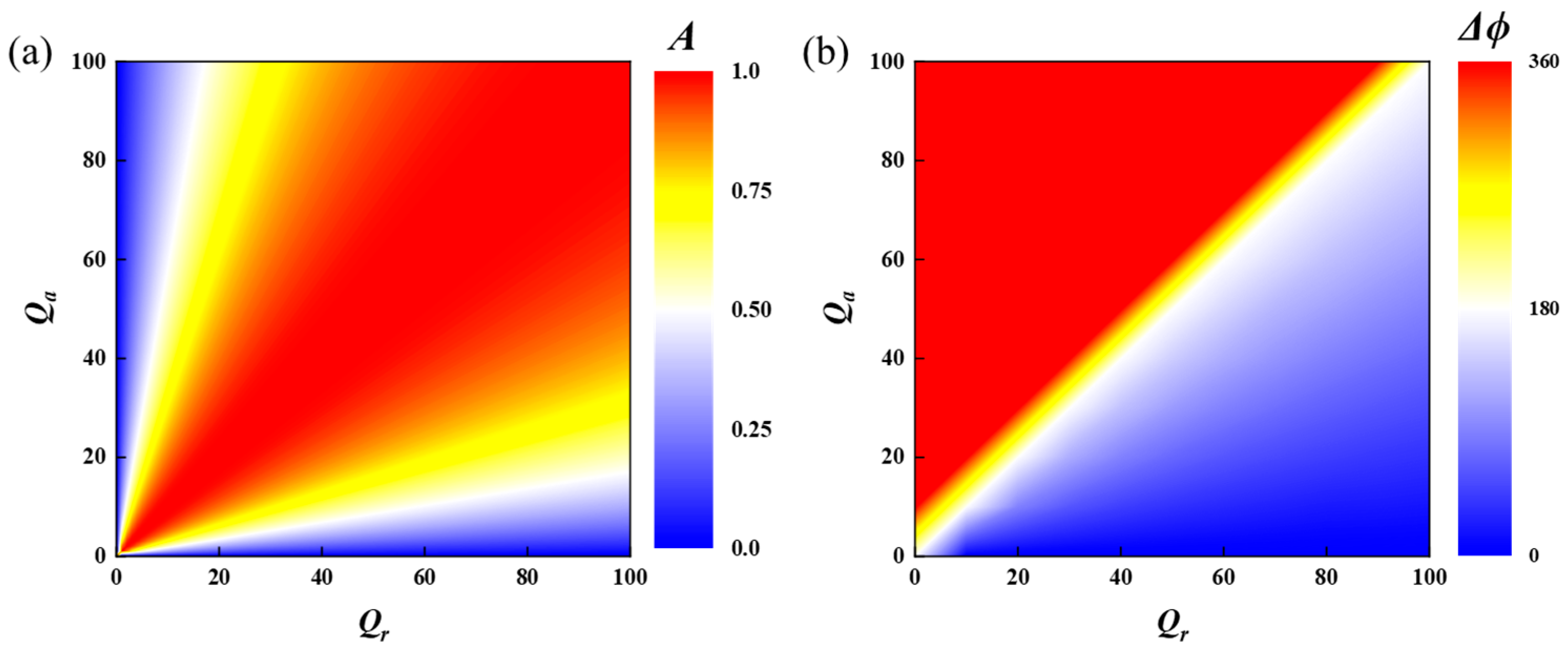
Figure 1a depicts a schematic of the variation of the model’s absorbance
2 with
and
at the resonance frequency. At that time, perfect absorption occurs, i.e.,
, and the absorbance decreases significantly when leaving this phase boundary. Meanwhile, we can distinguish between these two regions by comparing the range of variation of the reflection phase (ϕ) in different frequency domains, as shown in
Figure 1b. In the region where
>
, ϕ undergoes a continuous change from −80° to 180° as the frequency passes through the resonance due to the excessively small damping of the resonator and the weak internal absorption. On the contrary, in the region
<
, the variation of ϕ is small and less than 180° due to the excessive damping of the resonator.
Thus, the competition between the two Q-factors endows the MIM structure with a variety of physical properties suitable for different applications. For example, devices located in the > region can achieve phase modulation-related effects including polarization control and anomalous reflections, whereas the system with = behaves as a perfect absorber, and the resonator located in the < region is a simple electrical reflector.
A schematic of a typical MIM system is shown in
Figure 2, where the top metal layer consists of air slits (of width a) arranged with period d. The thicknesses of the metal and dielectric layers are hm and h. Simple analytical formulas for the radiative Q-factor can be derived for the structure under sub-wavelength (d ≪ λ, h < λ) and thin slit (a ≪ d) conditions:
where
is a dimensionless parameter measuring the contribution of the mth mode in the cavity,
is the permittivity of the spacer, and
describes the coupling between the external field and the mth internal mode. Based on the field distribution calculated by the MET (Method of Equivalent Transmission), the rigorously computed ratio of the total energy stored in the resonator to the energy radiated outside the resonator per oscillation cycle yields the Equation (7).
is defined as the ratio of the total energy U stored in the cavity to the energy absorbed by the dielectric spacer Pd and the metal Pm during the time oscillation period. Assuming that the field is uniformly distributed inside the cavity, U is proportional to the total volume of the cavity, hence
. Also, since
is a non-zero value, Pd is proportional to
. The field is proportional to the total volume of the cavity. Finally, considering the exponential decay of the electric field within the metal layer, i.e., the skinning depth, the metal absorption is proportional to the effective field decay length. Taking all factors into account, the final derivation can be made:
where α and β are the two parameters defining the relative contributions of dielectric and metallic media, respectively.
Through Equations (7) and (8), the MIM system performance can be effectively tuned by changing certain geometrical or material parameters of the metasurface. For example, decreasing the thickness of the spacer to reduce h can cause the system to transition from an underdamped region ( > ) to an overdamped region ( < ), each of which have different electromagnetic functions, and thus, we can understand that adjusting h can significantly change the properties of the metasurface.
In summary, transmitted surface plasma waves can be generated by excitation at the interface between the metal and the dielectric; however, their electromagnetic field decays rapidly near this interface. In layered MIM structures, when the thickness of the dielectric layer is small, surface plasma waves couple between the two interfaces of the metal and the dielectric, leading to the formation of symmetric and antisymmetric modes. Among these modes, the antisymmetric mode is not cut off at the limit where the thickness of the dielectric layer tends to zero, and this mode remains even when the dielectric layer almost disappears. This phenomenon shows that even small changes in the dielectric layer can have an important effect on the transmission of surface plasma waves, and therefore the effect of the thickness of the dielectric layer on the mode coupling and the transmission of surface plasma waves needs to be taken into account when designing layered MIM structures.
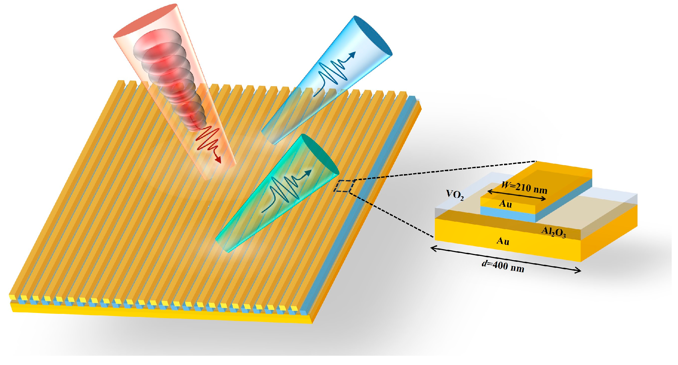
The MIM structure used in this paper is shown in
Figure 3, and the optimal structural parameters are determined according to the simulation results, which are in order from the top to the bottom, as follows: A gold (Au) stripe with a thickness of 40 nm is used as the metal coupling layer, and a 40 nm stripe of VO
2 is added to the second layer—and the complex refractive index of the VO
2 can be drastically changed with the temperature, which can realize the insulator–metal phase transition—the third layer is an Al
2O
3 dielectric layer with a thickness of h = 50 nm, and the last layer is a gold backing plate substrate with a thickness of 150 nm, which can play a role in stopping the light energy leakage from the bottom. The width of the metal stripes is w = 210 nm, and the minimum width of the periodic array is d = 400 nm. Incorporating the active substance (VO
2) directly into the MIM structure enhances the interaction between the active dielectric and the strong confinement field, and the induced phase transition of the VO
2 thin film produces a strong perturbation to the magnetic dipole resonance of the metasurface support.
Defining the reflectivity , the resonance absorption peak can be obtained through numerical calculation, and the coupling efficiency reaches the highest at the resonance absorption peak, where the reflected light part of the incident light and the leakage part of the waveguide guiding mode just reach the coherent phase cancellation, so that the reflectivity reaches the lowest, and the larger PSHE shift can be achieved here.
In this paper, the vortex beam carrying OAM is used as the incident light. Compared with the conventional Gaussian beam, the vortex beam is characterized by a constantly changing intensity distribution in its cross-section in the propagation direction and a complex phase structure. Due to the special nature of its phase and amplitude distributions, the angular momentum carried by the photons can interact with the structures in the medium during the propagation process, resulting in a change in the spin angular momentum of the photons and making the PSHE more significant.
3. Results
The PSHE on the metasurface of a VO2-based MIM structure in the near-infrared wavelength band is modeled by simulation. Firstly, a detailed model of the MIM structure is established and key structural parameters, such as layer thickness and geometry, are determined. Secondly, the material parameters of the different layer media are introduced, and the corresponding material dispersion models are established to more accurately describe the propagation behavior of light in the structure. By using an electromagnetic simulation calculation tool, we can obtain the reflection coefficients of the designed structure at different incident frequencies. These reflection coefficients provide an exhaustive understanding of the performance of the structure, including its optical response at different frequencies. Finally, in combination with the PSHE shift formula, we can calculate the surface PSHE shift of the MIM structure.
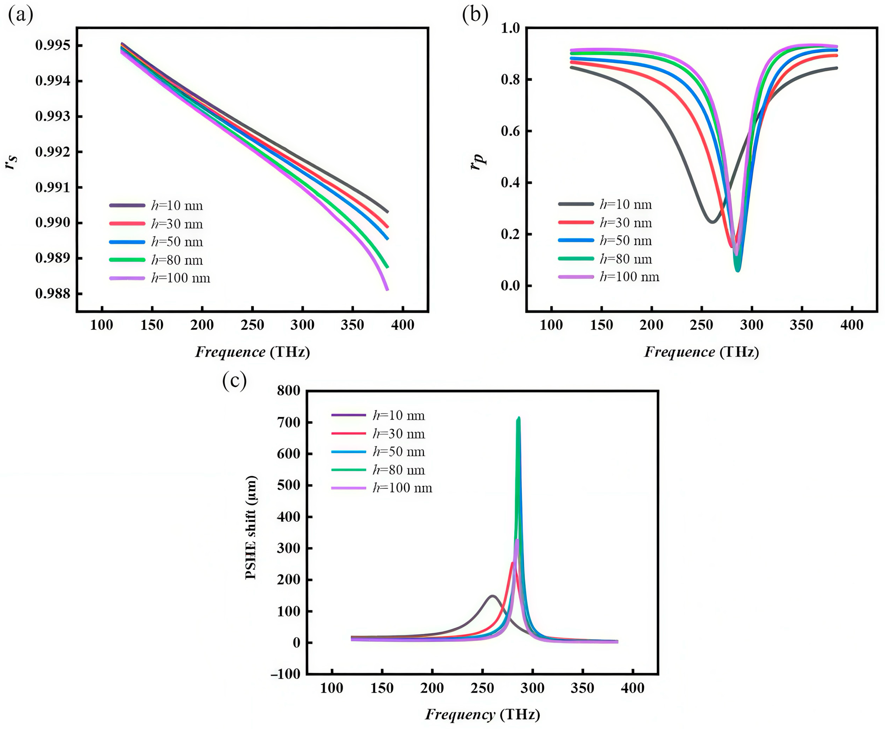
Adjusting the structural parameters of MIM metasurfaces directly affects their properties, such as reflection coefficients. In the structure of MIM metasurfaces, the thickness of the dielectric layer, h, and the width of the metal stripes, w, are two crucial parameters. Firstly, the propagation mode of electromagnetic waves in the metasurface can be changed by appropriately adjusting the thickness h of the dielectric layer, which in turn affects the reflection and transmission effects. By increasing or decreasing the thickness of the dielectric layer, we can adjust the phase delay of the metasurface, which changes the phase and amplitude of the reflected light and thus affects the manifestation of the PSHE. Secondly, the width of the metal stripe w is also one of the important parameters regulating the performance of the metasurface. The width of the metal stripe determines the local equivalent dielectric constant of the metasurface, which affects its reflection properties. By varying the width of the metal stripe, we can regulate the response of the metasurface to different wavelengths of light and optimize its reflection efficiency and the performance of the PSHE in specific wavelength bands.
Figure 4 shows the simulation results for varying the thickness h of the dielectric layer. In the case of metal stripe width w = 200 nm, h = 10, 30, 50, 80, 100 nm, the reflection coefficient
and
with the incident frequency change spectra are shown in
Figure 4a and
Figure 4b, respectively, the trend is relatively smooth in the whole range of change, the change is not obvious with the increase of h, and the valley of the value first increases and then decreases with the increase of h. The peak value of the PSHE shift curve, corresponding to that shown in
Figure 4c, also shows the increase and then decrease trend. Corresponding to the PSHE shift spectrum curve shown in
Figure 4c, the peak value also shows a trend of increasing and then decreasing, and the PSHE shift can reach 730
at h = 50 nm, which is much larger than 150
corresponding to h = 10 nm. It is verified that the thickness of the dielectric layer affects the performance of the MIM metasurface structure, which further has a modulating effect on the PSHE.
The explanation of this phenomenon can be derived from the working principle of MIM metasurfaces. Changes in the thickness of the dielectric layer change the distribution of the electromagnetic field in the metasurface, thus affecting its reflection characteristics. When the dielectric layer is thin, the electromagnetic field is more likely to couple between the dielectric layer and the metal layer, resulting in insignificant changes in the reflection coefficient. With the increase of the thickness of the dielectric layer, the electromagnetic field propagation path in the dielectric layer becomes longer, and the coupling effect is weakened, so that the reflection coefficient rp in the frequency change shows a more obvious trend. When the thickness of the dielectric layer continues to become larger and reaches an order of magnitude of the incident wavelength, the absorption of the p-polarized light by the metasurface is weakened, making the reflection coefficient larger.
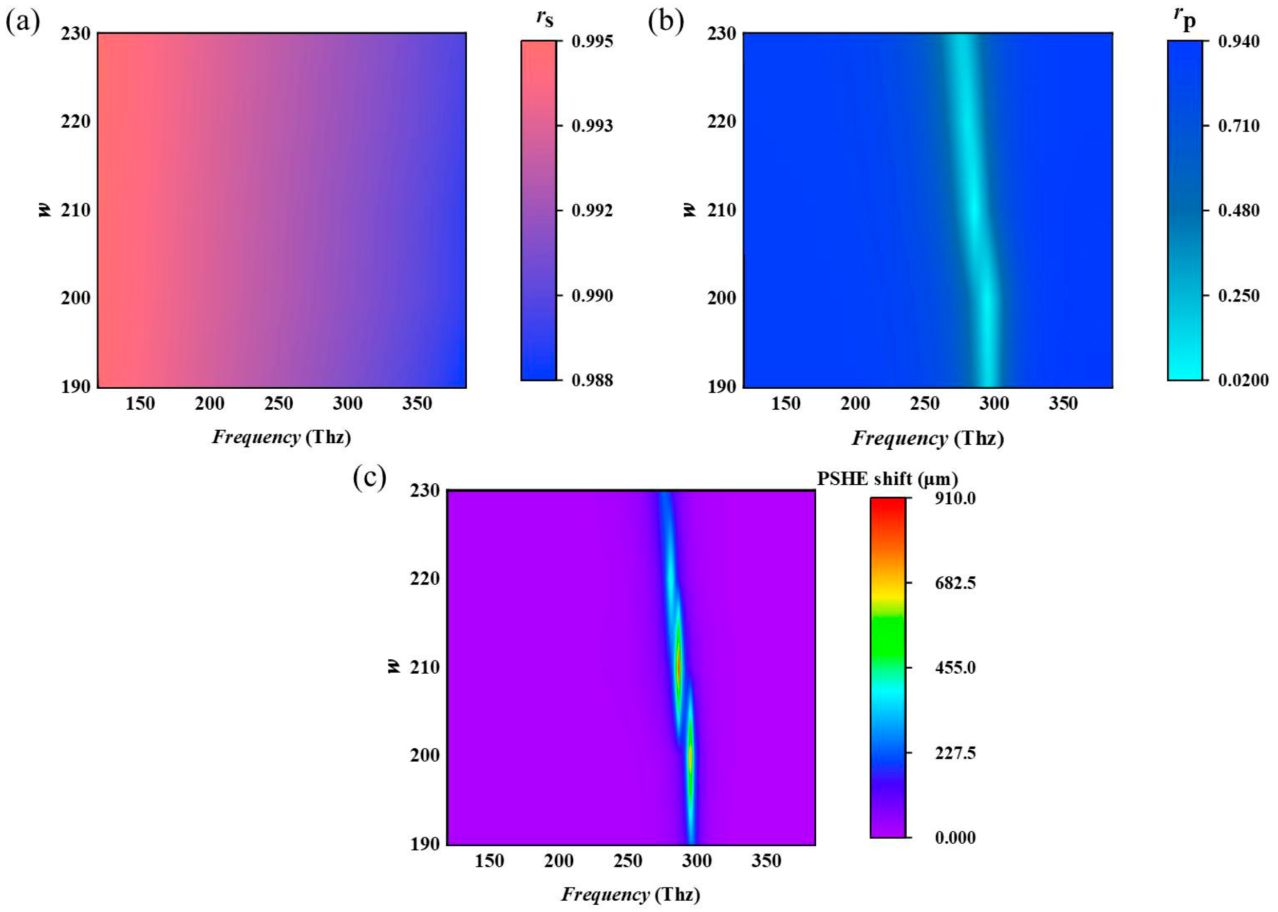
Next, another parameter affecting the structural properties is scanned, and
Figure 5 shows the simulation results of varying the width of the metal stripe w. The same steps are taken as before, the thickness of the dielectric layer is set to h = 50 nm, and w = 190, and 200, 210, 220, 230 nm is chosen. It is worth noting that the width of the VO
2 stripes is always the same as the width of the metal stripes, and the spectra of the reflection coefficients of the metasurface structure,
and
, concerning the change of the incidence frequency are shown in
Figure 5a and
Figure 5b, respectively. Similarly, the valley of the
exhibits a trend of increasing first and then decreasing. The peak value of its PSHE shift spectrum curve also shows a trend of increasing and then decreasing, and the PSHE shift reaches a maximum value of nearly 1000 μm at w = 210 nm, which is much larger than that of w = 190 nm, which is improved by nearly one order of magnitude. At w = 210 nm, this metasurface structure exhibits the strongest resonance for p-polarized light. This strongest resonance produces the largest phase gradient, which in turn induces the largest photonic spin Hall effect displacement.
When the width of the metal stripe is narrow, the local equivalent dielectric constant of the metasurface may be small, resulting in the electromagnetic wave propagation in the metasurface being restricted and the coupling effect being weak, and thus the absorption of the p-polarized light by the metasurface is relatively low and the reflection coefficient is slightly larger. As the width of the metal stripe increases, the local equivalent dielectric constant of the metasurface may increase, and the propagation path of the electromagnetic wave in the metasurface becomes wider, and the coupling effect is enhanced, leading to a decrease in the reflection coefficient. However, when the metal stripe width continues to increase, a certain critical width may be reached, beyond which the propagation path of the electromagnetic wave in the metasurface becomes too wide, leading to a weakening of the local effect, a limitation of the coupling effect, a weakening of the absorption, and a slight increase in the reflection coefficient valley again. Corresponding to the PSHE occurring on the surface of the structure also shows a corresponding trend.
In summary, the thickness of the dielectric layer and the width of the metal stripes jointly regulate the reflective properties of the MIM metasurface, and this process is also the process of determining the final optimal structural parameters that we mentioned earlier, i.e., the thickness of the dielectric layer is selected to be d = 50 nm, and the width of the metal stripes is selected to be w = 210 nm. Under this structural parameter, the designed MIM metasurface achieves the thermo-photonic modulation of the PSHE.
To verify the behavior of thermo-photonic modulation of the PSHE in MIM metasurface structures, the complex refractive index of VO
2 before and after the phase transition is measured by ellipsometry, and the structural parameter models are established when VO
2 is in different states, respectively. Before the phase transition, the lattice structure of VO
2 is a monoclinic phase, and at this time, the conductivity of VO
2 is extremely low, which is manifested as an insulating state; after the phase transition, the VO
2 is transformed from a monoclinic phase to a tetragonal rutile phase, and the conductivity increases by several orders of magnitude and behaves as a metallic state [
32,
33]. Since VO
2 is in between the metallic streak and the Al
2O
3 dielectric layer, it interacts with the Al
2O
3 below when it is in the insulating state and they act as a dielectric layer together; when VO
2 transforms to the metallic state, it is coupled with the gold layer. In this transformation process, the structural parameters change, and the reflection coefficient is bound to change accordingly.
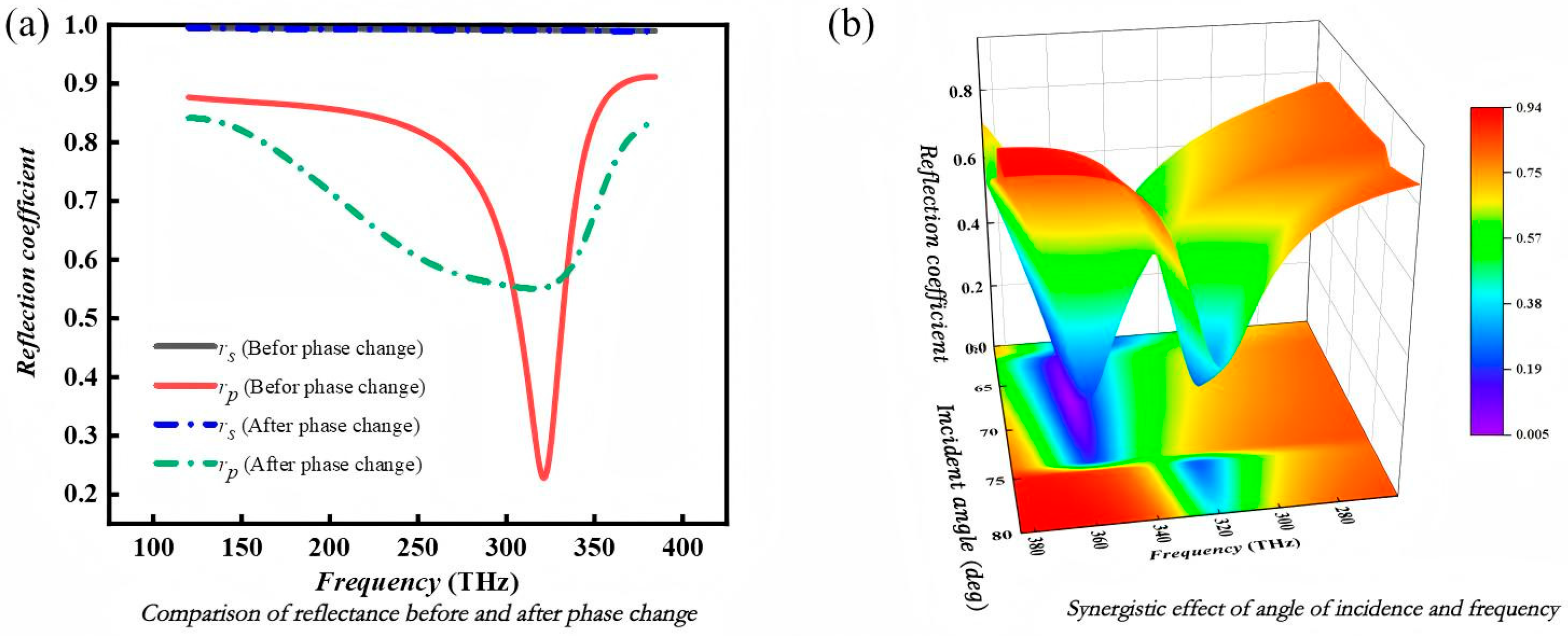
Figure 6a shows the spectra of the structural reflection coefficients of VO
2 before and after the phase transition with temperature change, from which it can be seen that before and after the phase transition of VO
2 occurs,
shows a valley value, while
is basically unchanged, but the difference between
and
before the phase transition |
| is obviously larger than that after the phase transition, i.e., the beam produces a larger shift of the PSHE on the surface of the MIM structure where VO
2 is in the insulating state than in the metallic state.
Figure 6b shows the three-dimensional schematic diagram of the variation of the reflection coefficient
of the MIM super-surface with the incident frequency and the incident angle before the phase transition of VO
2. The
shows an increasing tendency with the incident frequency (2.8 × 10
14–3.8 × 10
14 Hz) and the incident angle (60°–80°). From increasing and then decreasing trends and an overall perspective, two peaks appear near the incident frequency
, the incident angle
, incident frequency
, and incident angle
, and the former peak is significantly higher than that of the latter, which indicates that the MIM structure reflects the p-polarized light more lowly at the incident frequency and the incident angle corresponding to the former, where the PSHE is more obvious here.
Based on the above analysis, the incident wavelength
, corresponding to the incident frequency
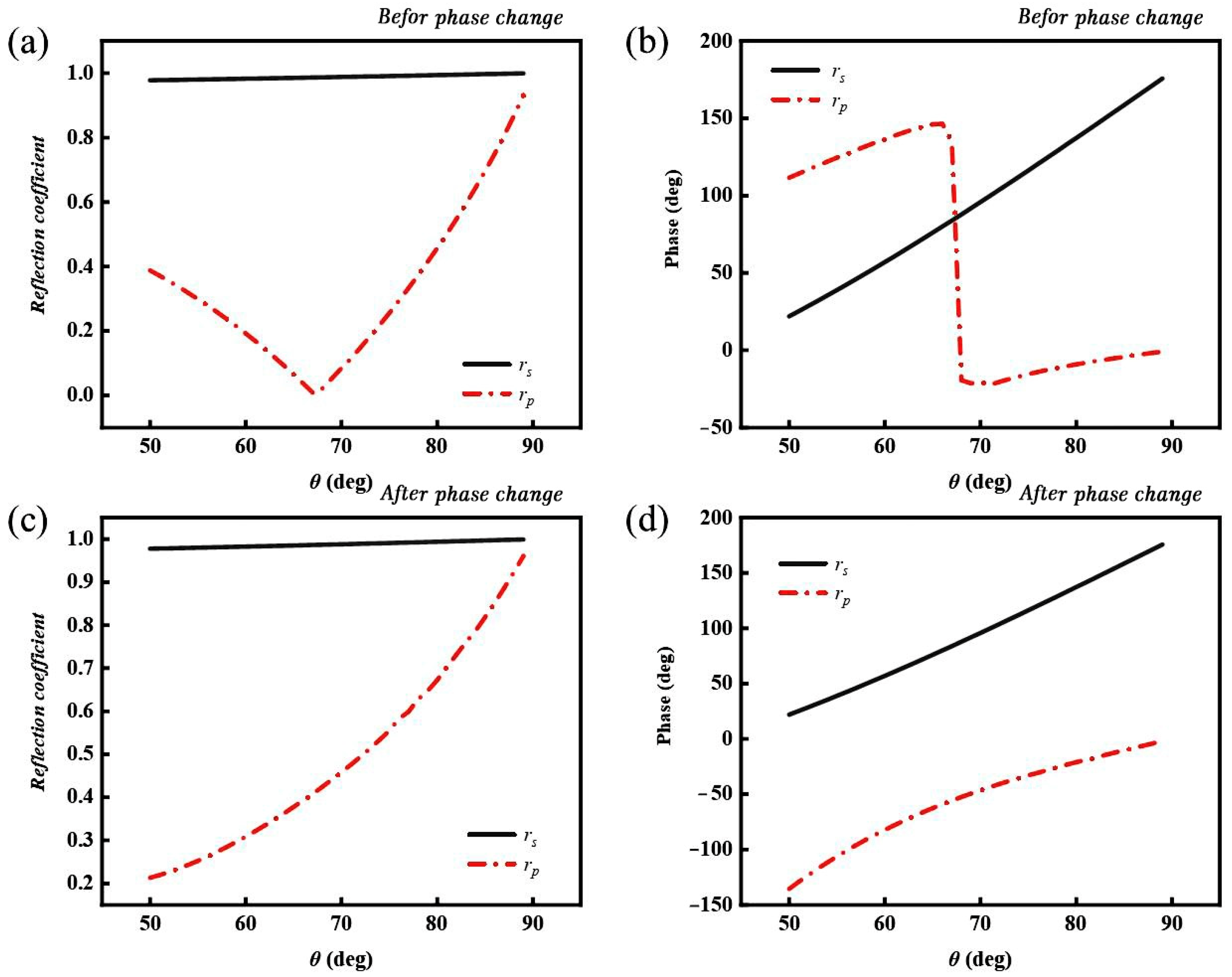
, was selected, and the incident angle θ was scanned for further analysis.
Figure 7 shows the spectral lines of the structural reflection coefficient amplitude and phase variation with the incident angle before and after the phase transition. When VO
2 does not undergo a phase transition, as in
Figure 7a,b, the p-polarized light is reflected and a reflection valley appears, and the phase changes abruptly at the same position, while the s-polarized light does not show any obvious change and, accordingly,
also peaks here. When VO
2 undergoes a phase transition and is in the metallic state, as in
Figure 7c,d, the reflection coefficient and phase as a whole show nearly linear changes.
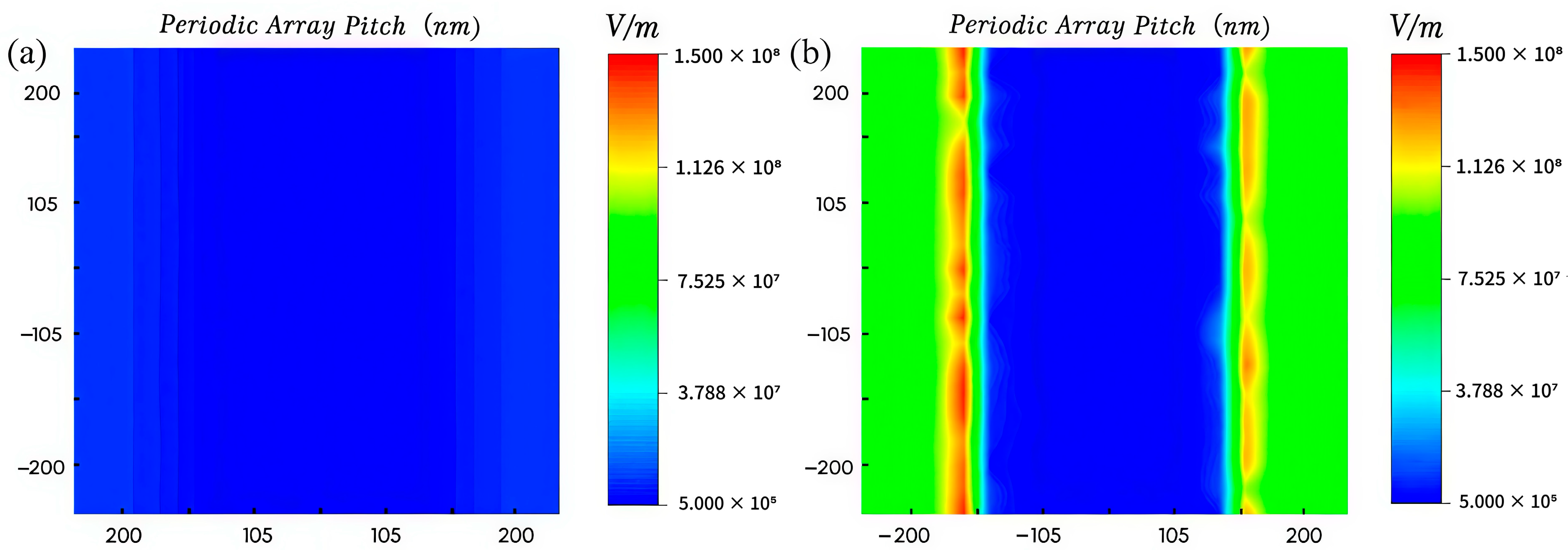
To further explain the reason for the trends presented in the reflection coefficient
and
curves, an electric field monitor is added during the simulation to observe the electric field distribution on the surface of the MIM structure, as shown in
Figure 8.
Figure 8a,b show the distribution of the electric field strengths in the TE and TM modes, i.e., in the s-polarized and p-polarized modes, respectively, and it can be seen that the electric field strengths of the surface in the p-polarized mode are much higher than those in the s-polarized mode. This indicates that the surface of the structure absorbs the p-polarized light more strongly, which results in lower reflectivity. This is due to the fact that the TM mode generates surface plasmon polariton (SPP) resonance on the surface of the structure. Surface-isotropic excitation is an electromagnetic phenomenon in which electrons and photons interact in the interface region between the metal and the medium, and when the intrinsic resonance frequency of free electrons in the metal is the same as the frequency of the electromagnetic wave incident on the metal surface, the two will be coupled to produce a resonance oscillation, forming a swift wave. In the MIM structure mentioned in this paper, when the incident light irradiates the surface of the metal grating, diffraction occurs due to scattering and interference, and the surface equipartition excitation effect is excited by using the diffraction of the surface metal stripes to satisfy the wavevector matching condition. The surface equipartition excitation resonance will have a great absorption effect on the incident light, thus generating a strong electric field on the metal surface.
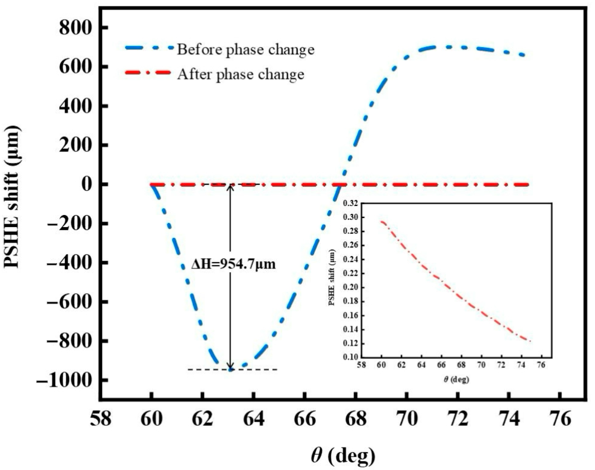
Figure 9 shows a schematic diagram of the PSHE shift on the surface of the MIM structure before and after the VO
2 phase transition. The solid line indicates the PSHE shift of the VO
2 structure in the insulating state, which corresponds to the reflection valley of the
curve, where the optical spin splitting reaches a great value, with to consecutive peaks, the valley value of 955
and the peak value of 705
, whereas the value of spin splitting of the surface of the VO
2 structure in the metallic state is very small, only a few micrometers. The phase transition of VO
2 with the change of temperature changes the whole structural parameter and the optical response. After the phase transition of VO
2 with temperature change, all the structural parameters are changed, and the optical response is changed, resulting in the rapid change of the PSHE shift, which plays a role in regulating the PSHE. The value of the PSHE shift before and after the phase transition, ΔH, reaches 954.7
, which is nearly eight times higher than the previous results of the simple layer structure, indicating that the thermo-photonic modulation of the PSHE by the MIM superstructure is more significant.
In the MIM metasurface structure, when VO2 is in the insulating state, it forms a dielectric layer together with the Al2O3 layer. In this state, incident light can trigger a magnetic dipole resonance, leading to a concentration of the electromagnetic field between the metal backplate and the top metal strip. In this case, the dielectric nature of the VO2 layer allows the electromagnetic field to be distributed within the structure. However, when the vanadium oxide is transformed to a metallic state, the effective thickness of the dielectric layer decreases, leading to a change in the distribution characteristics of the electromagnetic field. At this point, the dominant electromagnetic field is confined to the Al2O3 layer, as the conductivity of the VO2 layer increases, making it a barrier to the electromagnetic field. This transition leads to a significant change in the electromagnetic properties of the structure, which is manifested as a change in the distribution of the electromagnetic field within the dielectric layer, thus affecting the overall performance of the metasurface structure.


 ,
, 