Article

Induced Effects of Nano-Patterned Substrates on the Electrical and Photo-Electrical Properties of PTB7-Th:ICBA (1:1, wt.%) Bulk-Heterojunction Solar Cells

1
Faculty of Physics, University of Bucharest, 405 Atomistilor Street, 077125 Bucharest-Magurele, Romania
2
Institute of Condensed Matter and Nanosciences (IMCN), Universite Catholique de Louvain (UCLouvain), Place Croix du Sud 1, B-1348 Louvain-la-Neuve, Belgium
3
Academy of Romanian Scientists (AOSR), Ilfov Street 3, 050045 Bucharest, Romania
4
National Institute of Material Physics, 405A Atomistilor Street, 077125 Magurele, Romania
5
National Institute for Lasers, Plasma and Radiation Physics, 409 Atomistilor Street, 077125 Magurele, Romania
*
Authors to whom correspondence should be addressed.
Surfaces 2025, 8(2), 30; https://doi.org/10.3390/surfaces8020030
Submission received: 20 February 2025 / Revised: 1 April 2025 / Accepted: 16 April 2025 / Published: 1 May 2025
(This article belongs to the Collection Featured Articles for Surfaces)

Abstract

In this study, we detailed the fabrication and characterization of photovoltaic structures based on PTB7:ICBA (1:1, wt.%) bulk-heterojunction on optical glass substrates by spin-coating. Some samples were deposited on a flat substrate, and others were placed on a patterned substrate obtained by nano-imprinting lithography; the induced effects were analyzed. We demonstrated that using a patterned substrate enhanced the maximum output power, primarily because the short-circuit current density increased. This can be considered a direct consequence of reduced optical reflection and improved optical absorption. The topological parameters evaluated by atomic force microscopy, namely, the root mean square, Skewness, and Kurtosis, had small values of around 2 nm and 1 nm, respectively. This proves that the mixture of a conductive polymer and a fullerene derivative creates a thin film network with a high flatness degree. The samples discussed in this paper were fabricated and characterized in air; we can admit that the results are encouraging, but further optimization is needed.

Graphical Abstract

1. Introduction

The tendency to replace solar devices based on silicon technology with other similar but eco-friendly materials and production techniques has advanced enormously during the last twenty years. The search for alternate materials and configurations led to the optimization of the CdTe/CdS heterojunction and power conversion efficiencies (PCEs) of almost 17% being reached [1], but efficiencies of around 24% are expected [2]. In 2022, S. Dursun et al. reported an efficiency of 22% [3]. Another route was the development of perovskite-based architectures, with remarkable features such as high PCE values (around 25%) and improved time stability compared to organic photovoltaic cells (OPVs) [4]. On the other hand, OPV technology offers several advantages such as relatively reduced financial costs derived from using common deposition techniques and the large possibility of building customized materials in a straightforward manner. Moreover, different processes can be used to improve light harvesting in OPVs and thus increase their efficiency; one of these processes, which was recently investigated, is electrode nano-structuring [5].
Generally, as the active layer, OPVs have a bulk-heterojunction blend between a regio-regular polymer, the donor material, and a fullerene derivative, the acceptor [6]. One of the most studied mixtures involves P3HT:PC60BM (or PC70BM, PC71B), poly(3-hexylthiophene-2,5-diyl), and [6,6]-phenyl C60 (C70, C71) butyric acid methyl ester [6,7]. Recently, special attention was paid to PTB7-Th, poly [4,8-bis(5-(2-ethylhexyl)thiophen-2-yl)benzo [1,2-b;4,5-b′]dithiophene-2,6-diyl-alt-(4-(2-ethylhexyl)-3-fluorothieno [3,4-b]thiophene-)-2-carboxylate-2-6-diyl], which has a narrow LUMO–HOMO difference compared to P3HT, namely 1.58 eV, and is more stable in ambient atmospheres (LUMO—Lowest Unoccupied Molecular Orbital; HOMO—Highest Occupied Molecular Orbital) [8]. ICBA, indene-C60 Bissaduct, has a LUMO energy level 0.17 eV higher than that of the PCBM family, and this provides superior open-circuit photovoltage and an increase in the PCE [9]. The enhanced photovoltaic performances of PTB7-Th and ICBA were recognized by their usage in different architectures. Thus, A.R. Tetreault reviewed the PTB7 polymer class and demonstrated its potential in different OPV architectures (with various buffer/injection layers) [10]. Also, blends of this polymer and ICBA were studied for printable solar windows [11] or for other optoelectronic applications [12]. Despite the achievements, the number of references about the PTB7-Th: ICBA mixture is low [13,14], and heterojunctions built with such materials on nano-patterned substrates are few [15,16]. The use of a customized substrate, in the highly ordered sense, has only been exploited in recent years, and the results obtained are truly encouraging [17,18,19]. Among the technologies available for the micro-/nano-patterning of deposition substrates, the most used are photolithography and electron beam lithography (EBL) [20]. However, these techniques have some disadvantages: one cannot be applied to create nano-patterns, and the other one is not suitable for large surfaces. Instead, the UV nano-imprint lithography (UV-NIL) technique is a low-cost, high-throughput method for patterning substrates, including plastic ones [21]. Practically, UV-NIL can be used on rigid/flexible substrates to produce (even on large surfaces) patterns with different shapes or sizes [19]. Reports on the involvement of the UV-NIL technique in the nano-structuring of OPV electrodes are available in the literature [19,22,23].
In this context, this paper discusses the PTB7-Th:ICBA bulk-heterojunction blend’s performance on two different optical glass substrates, one flat and the other highly ordered. The nano-patterned substrate was developed by nano-imprint lithography. Our assumption that arranged substrates can affect the photovoltaic performances were confirmed by the increased determined values of their specific parameters.

2. Materials and Methods

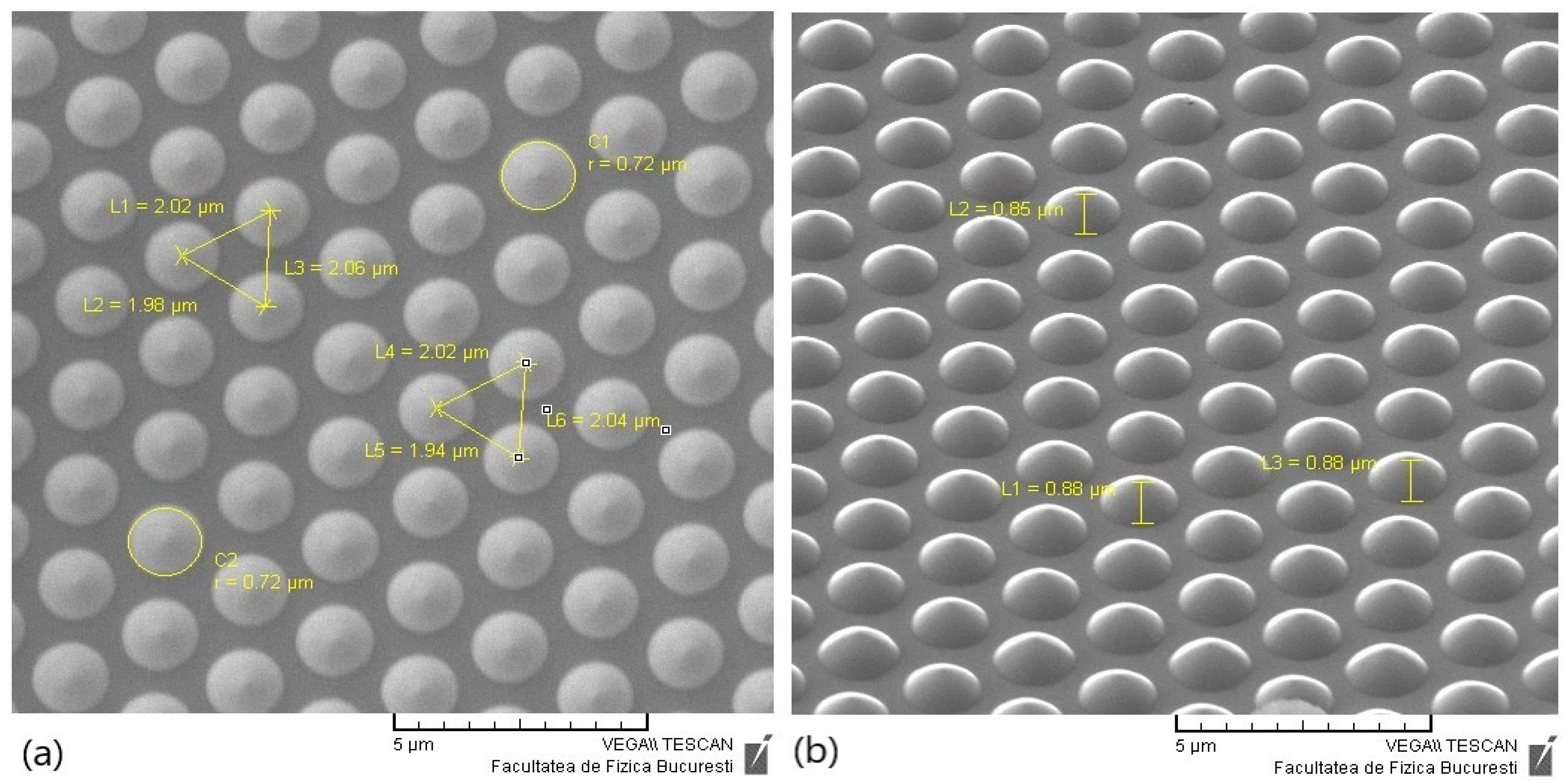
2.1. Sample Preparation

Photovoltaic devices based on poly [4,8-bis(5-(2-ethylhexyl)thiophen-2-yl)benzo [1,2-b;4,5-b’]dithiophene-2,6-diyl-alt-(4-(2-ethylhexyl)-3-fluorothieno [3,4-b]thiophene-)-2-carboxylate-2-6-diyl] (Ossila Ltd., Sheffield, UK), CAS number: 1469791-66-9, denoted here as PTB7-Th, as the donor material, and indene-C60 Bissaduct (Merck SA, Darmstadt, Germany), CAS number: 1207461-57-1, denoted here as ICBA, as the acceptor material, were fabricated onto optical glass substrates (microscope slides). Prior to any deposition, the optical glass substrates were subsequently cleaned in acetone (Merck SA, Darmstadt, Germany), with a CAS number of 67-64-1, in isopropanol (Merck SA, Darmstadt, Germany), with a CAS number of 67-63-0, and in deionized water. The samples were dried under nitrogen flow. The general architecture of the photovoltaic structures obtained was glass/ITO/PEDOT:PSS + GO (1 mL:1 mL)/PTB7-Th:ICBA (1:1, wt.%)/LiF/Al, but the glass/ITO anode was customized as flat or nano-patterned. The patterned positive electrode was obtained by nano-imprinting lithography (NIL). The process consists of pressing a stamp with the inverted copy of the desired patterns onto the substrate, covered with a negative photoresist. This is then solidified by applying UV radiation. In our case, an EVG UV-A2 (EVG Group, St. Florian am Inn, Austria), 200 nm resist was deposited at 2000 rpm for 60 s onto glass substrate by spin-coating. The nano-imprint process was performed onto a mask aligner EVG 620 NT (EVG Group, St. Florian am Inn, Austria) with an NIL module used for resist curing 22 mW/cm2 for 60 s. The geometrical features of micro hillocks were chosen in such a way as to avoid capillarity effects. A Scanning Electron Microscopy (TESCAN Group, a.s., Brno-Kohoutovice, Czech Republic) (SEM) micrograph is shown in Figure 1 together with the geometrical features of the fabricated micro hillocks. The glass/ITO flat anode was obtained by directly growing ITO onto an optical glass substrate, following the procedure described below.
The ITO films were deposited by the Pulsed Laser Deposition technique using an excimer laser source with KrF* (Coherent Corp., PA, USA, CompexPro 205, 248 nm wavelength, τFWHM~25 ns), operating at a 10 Hz repetition rate. A solid ITO target (SCI Engineered Materials, OH, USA, In2O3:SnO2 = 90%:10% weight) was ablated with 8000 laser pulses. The laser beam was directed on the surface of the target at an incidence angle of 45° with a MgF2 lens (300 mm focal length) located outside of the deposition chamber. The distance between the target and the substrate was fixed at 7 cm. In order to prevent local damage, the target was continuously rotated during the deposition process. Oxygen was used as a reactive gas, with the oxygen pressure being 1.5 Pa. The laser fluence was 1.2 J/cm2.
The PEDOT:PSS (poly(3,4-ethylenedioxythiophene) polystyrene sulfonate (Ossila Ltd., Sheffield, UK, CAS number: 155090-83-8) material is a heavily doped p-type semiconductor, acting as Hole Transport Layer (HTL) in electronic and optoelectronic devices, such as photovoltaic cells [24], electrochemical transistors [25], and sensors [26]. Its special properties are related to the compensation of holes on the PEDOT+ chains by the sulfonate anions on the PSS-; PSS- acts as a dopant [27]. On the other hand, graphene oxide (GO) is a 2D structure, manifesting as a single layer of carbon atoms covalently functionalized with oxygen [28]. These functional groups allow GO to disperse easily in water [29]. Because both PEDOT:PSS and GO are aqueous solutions, the HTL was prepared as a mixture between 1 mL of PEDOT:PSS and 1 mL of GO. The PEDOT:PSS + GO layer was deposited onto the glass/ITO front electrode by spin-coating at 2000 rpm for 40 s. First, the PEDOT:PSS solution was filtered through a 0.45 µm PFTE filter. The fabricated films were subjected to thermal treatment in an oven in air conditions at 100 °C for 30 min to eliminate the water traces. Graphene oxide was purchased from Merck SA, Darmstadt, Germany.
The active layer was prepared as a (1:1, wt.%) mixture between PTB7-Th and ICBA; 10 mg of PTB7-Th and 10 mg of ICBA were dissolved in 1 mL of 1,2-dichlorobenzene (Merck SA, Darmstadt, Germany), Beilstein number: 606078. The stirring time of this solution before deposition was 5 h. The fabrication of the active layer was a two-step spin-coating process performed at 1500 rpm for 40 s, followed by 2000 rpm for 20 s. Thermal treatment was performed immediately after deposition in an oven, in air conditions, at 90 °C for 30 min. Thermal treatment removes the solvent traces and, for some polymers, initiates a pre-crystallization process, leading to an elementary arrangement of polymeric chains [30]. The spin coater machine is a Brewer Science CEE 2000 (MO, USA) with a maximum spin speed of 6000 rpm.
The lithium fluoride (LiF, Merck SA, Darmstadt, Germany, CAS number: 7789-24-4) and the aluminum (Al) cathode were prepared by thermal evaporation at a working pressure of 8 × 10⁻⁵ bar, a substrate temperature of 30 °C, and a source temperature of 425 °C.
All chemicals were used without further purification and are commercially available.
The thickness of deposited layers was determined, either by profilometry (P) or by quartz crystal microbalance (QCM), and the values are presented in Table 1.
The evaluation of thickness by profilometry consists of taking several measurements in different parts of the sample; the indicated value is an average of collected data.

2.2. Sample Characterization

The atomic force microscopy (AFM) images of the active blend PTB7-Th:ICBA (1:1, wt.%) were acquired using an A.P.E Research s.r.l. (Trieste, Italy) machine working in a non-contact mode, in air, at room temperature.
For the Scanning Electron Microscopy (SEM) analyses, a Tescan Vega XMU-II (Brno-Kohoutovice, Czech Republic) machine was used, working at an accelerating voltage of 30 kV.
The optical characterization was performed by a UV-Vis 750 Lambda PerkinElmer (CT, USA) device, in air, at room temperature.
The quartz crystal microbalance system is a Tectra GmbH device (Frankfurt, Germany).
The thickness was measured using an Ambios XP-100 Stylus Surface Profiler (MT, USA), which is now part of KLA-Tencor Corp. (AZ, USA). This profiler has a stylus with a 2.5 µm radius and a force range of 0.03–10 mg. It can create surface profiles and measure soft films and substrates without damaging the surface, with step heights that can range from less than 50 Ångströms to as much as 1.2 mm.
The electrical and photo-electrical measurements were performed in dark and AM 1.5 conditions (incident power of 100 mW/cm2) using a Keithley 2400 Sourcemeter (Tektronix Ltd., Oldbury, UK) and a Newport Oriel (Artisan Technology Group, Champaign, IL, USA) solar simulator. To evaluate the generated photocurrent of fabricated photovoltaic structures at a certain incident wavelength, a Newport Oriel monochromator was used too.

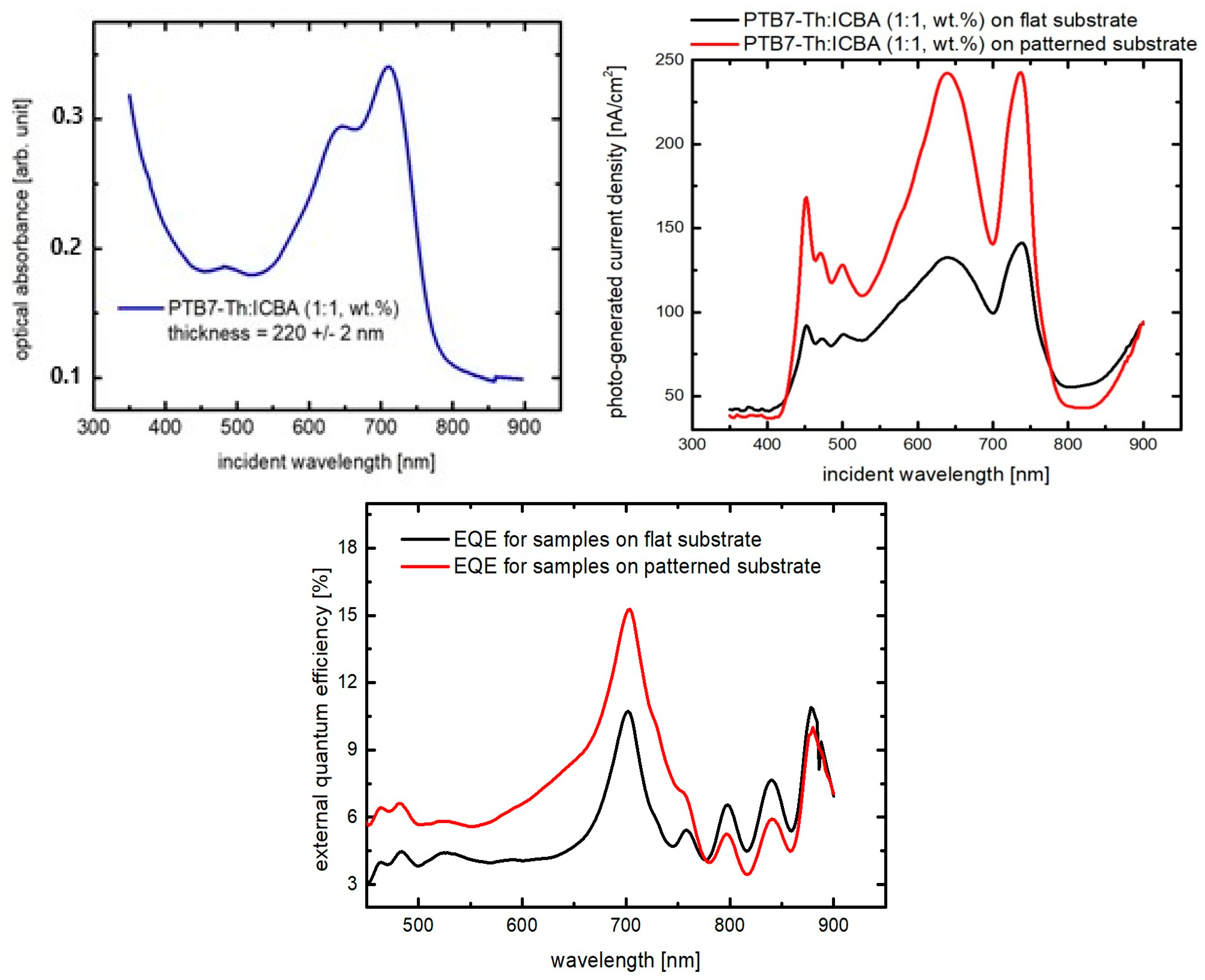
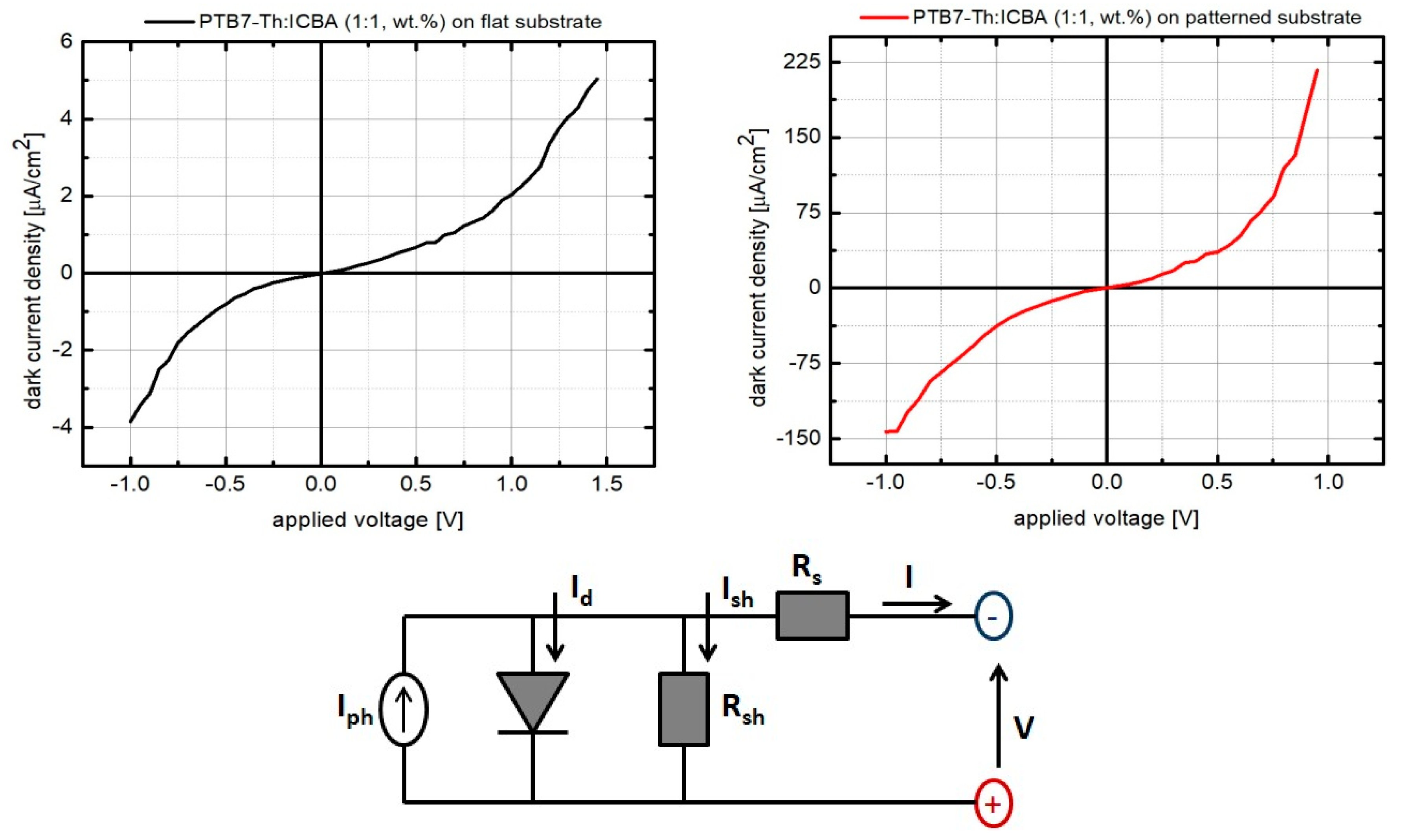
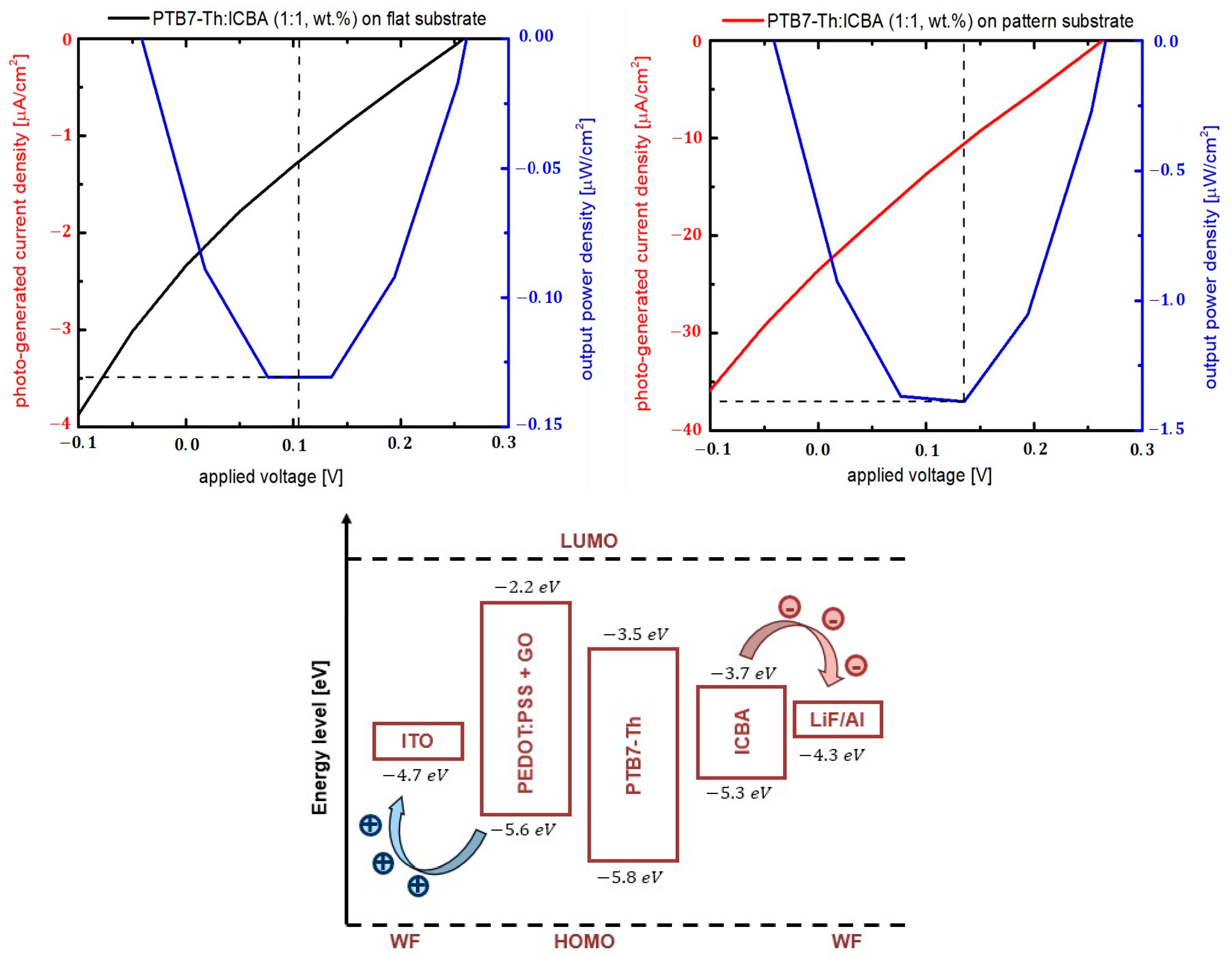
3. Results and Discussions

The AFM images of the PTB7-Th: ICBA (1:1, wt.%) active layer are shown in Figure 2. The scanned areas were 5 µm × 5 µm and 1 µm × 1 µm. The metrological parameters such as root mean square roughness, Skewness, and Kurtosis were assessed for the 25 µm2 scanned area, and the 1 µm2 zone was analyzed more in the context of a preliminary crystallization process; upon careful examination, an alignment of the majority of peaks over an imaginary 45° line in the (x, y) plane of an arbitrary Cartesian reference system seems to appear. Unfortunately, the X-ray diffraction measurements did not confirm this hypothesis; the results obtained were not included in this paper.
For the flat substrate, the surface topography showed a root mean square roughness of 2 nm, and Skewness and Kurtosis values of less than 1 nm. These parameters’ small values indicate the very good miscibility of the conductive polymer (PTB7-Th) and fullerene derivative (ICBA), which leads to smooth and uniform films. The Skewness parameter shows the asperity of the film’s surface [31], and its slightly positive value suggests the very good planarity of the surface and the predominance of not-high peaks over valleys. The confirmation that the PTB7-Th:ICBA (1:1, wt.%) active layer is smooth and flat is given by Kurtosis values; a value of 0.3 describes a surface with almost no extremes.
The patterned substrate’s highly arranged architecture and uniform coverage with the active layer are confirmed by the Skewness and Kurtosis parameters, 0.56 and −0.8, respectively.
The absorbance spectroscopy spectrum of the active layer is presented in Figure 3, together with the measured density photo-generated current, for both the patterned and non-patterned samples. The active area of the obtained samples was 0.4 cm2.
The PTB7-Th polymer has a broad absorption between 600 and 800 nm and the peak close to 500 nm is assigned to the ICBA fullerene derivative. The use of such blends composed of conductive polymers and fullerene derivatives offers the enlargement of the absorption domain compared to individual layers [32]. The correspondence between the absorption peaks and the photo-generated current maxima can be observed in the right-side graph. The photo-generated current for the samples deposited onto the patterned glass substrate is two times larger than that obtained for the flat samples. We assume this increase in the photo-generated current may be related to an increase in optical absorption due to the reduction in reflection. Similar results were reported by Liu et al. for nano-patterned Si substrates. Also, Clampory et al. showed similar results, focusing on the influence of patterned transparent conductive oxide on some electrical and photo-electrical parameters such as the series resistance and fill factor [33,34]. To support our assumption, we calculated the external quantum efficiency and obtained a value of around 15% for the devices on the patterned substrate and one of around 11% for the devices on the flat substrate. The indicated values were considered for a wavelength of 702 nm, the same wavelength for which the maximum optical absorption was obtained. The EQE is the ratio between the number of electron–hole pairs generated and the number of incident photons. The obtained results indicate that an increased number of electron–hole pairs is created, enhancing the maximum output power for patterned samples.
The architecture of any photovoltaic cell contains two parasitic resistances, the series and shunt resistances. Figure 4, together with the appropriate circuit diagram, displays the diode-like response of our fabricated devices in the dark. Table 2 summarizes the determined electrical parameters for the prepared samples. The forward bias was considered for glass/ITO as the anode and LiF/Al as the cathode.
The series resistance (Rs) is affected by several factors, such as the electrical mobility of component layers, cell dimensions, especially the thickness of the whole architecture, and charge carrier concentration, and the shunt resistance (Rsh) offers information about the photocurrent losses due to the existence of alternate paths for the photo-generated charge carriers, particularly the recombination of electron–hole pairs. The ideality factor of a diode (n) is a measure of how well the device is working by evaluating the deviation from the ideal diode equation. For the photovoltaic devices fabricated on a flat substrate, the Rs and Rsh have close values. The MΏ range of the series resistance indicates a low-recombination process, and we presume it takes place at the interfaces, mainly at the active layer/back contact juncture. This information was supported by the dark current–voltage curves, which do have not a high degree of asymmetry. Even if the value of the series resistance is significantly smaller, the current–voltage dependence of nano-patterned devices in the dark has a similar shape, characterized by low asymmetry. This behavior can be a direct consequence of a smaller concentration of point-like defects at interfaces. On the other hand, if we compare the evaluated R s h values for both types of devices, one may consider it as contradictory behavior. However, we should notice that the good performance of a photo-element implies small values of the series resistance and large values of the shunt resistance. For the nano-patterned photovoltaic cells, the shunt resistance is one order of magnitude higher than the series resistance and this is sustained by its better photo-electrical operation.
An ideality factor close to 1 implies reduced recombination compared to non-patterned samples, which means a better working diode, and thus a better conversion of solar radiation into direct electrical current.
The photo-electrical behavior of the obtained samples, namely the current–voltage characteristics in AM 1.5 conditions (incident power of 100 mW/cm2) together with the energy band diagram of component materials, is displayed in Figure 5. The same bias was maintained as for the electrical measurements. The calculated photo-electrical parameters are displayed in Table 3 for nano-patterned and flat developed devices.
One may observe that enhanced photovoltaic performances were obtained for devices on nano-patterned substrates. The calculated power conversion efficiency (PCE) was 0.08 × 10 3 % for the samples developed on a flat substrate and 1.03 × 10 3 % for those on a patterned substrate. Although we report small values of PCE, one may observe a significant increase in it for those devices on patterned substrates. Such small values are the direct consequence of fabrication in an ambient atmosphere. This reinforces the initial assumption of this study—a highly ordered substrate leads to an increase in the photo-generated current. We consider this behavior to be related to the creation of well-defined percolation paths for the charge carriers; together with a reduced recombination process, these can raise the output power. The difference in maximum output power of one magnitude degree is due to the ten times larger photo-generated current, and this is a direct consequence of the better collection of photo-generated charge carriers at the electrodes. The overall photovoltaic achievements can be improved by creating patterns and following their shape, even if such materials have a poor crystalline arrangement. Of course, there is plenty of room to optimize not only the properties of component materials but, also, the geometrical features of nano-patterns.
Moreover, one of the issues photovoltaic devices based on organic materials face is their time stability, which is poor if non-encapsulated samples are exposed to moisture and oxygen. The pristine fabricated devices were stored in the dark, in an ambient atmosphere, and at room temperature and tested in AM 1.5 conditions six months after preparation. The obtained results indicated no photovoltaic response, while the dark current–voltage characteristics showed the diode’s specific shape.

4. Conclusions

Photovoltaic devices based on the PTB7-Th:ICBA (1:1, wt.%) were fabricated onto optical glass substrates. These were flat or patterned and were obtained by nano-imprinting lithography. Their electrical and photo-electrical performances were analyzed by current–voltage measurements in the dark and AM 1.5 conditions. The photo-generated current density of the devices fabricated onto the nano-patterned substrate was one order of magnitude higher, J s c = 26.3   μ A / c m 2 compared to 2.35   μ A / c m 2 , and this led to a similar increased in the maximum output power, P m a x = 1.03   μ W / c m 2 , compared to P m a x = 0.08   μ W / c m 2 . This behavior may be due to a reduction in optical reflection and an increase in optical absorption. Despite this improved photo-electrical performance, the current–voltage characteristics in the dark showed poor asymmetry for both types of devices, but with significantly smaller value of the series resistance for nano-patterned samples. This can be assumed to be a direct consequence of lower activity in terms of recombination processes due to a lower concentration of point-like defects at the interfaces.
The small values of the topological parameters evaluated using the atomic force microscopy demonstrate that the nano-patterned substrates of such geometry can be used for these types of optoelectronic applications.
As a general conclusion, we may consider that the overall photovoltaic performances of the nano-patterned devices were enhanced, but future studies are needed to develop a direct relationship between the geometrical features of patterns and the photovoltaic structures’ performances.

Author Contributions

Conceptualization, S.I. and O.R.; methodology, T.S. and S.A.; software, V.-A.A.; validation, S.I., M.S. and O.R.; formal analysis, T.S. and M.C.B.; investigation, T.S., I.S. and G.S.; resources, T.S. and M.C.B.; data curation, S.I.; writing—original draft preparation, S.I., T.S. and S.A.; writing—review and editing, S.I. and O.R.; visualization, S.I., O.R. and M.S.; supervision, S.I. and O.R.; project administration, S.I. and O.R.; funding acquisition, O.R. and M.S. All authors have read and agreed to the published version of the manuscript.

Funding

This research was funded by the Romanian Ministry of Research, Innovation and Digitalization, CNCS-UEFISCDI by project number PN-III-P4-ID-PCE-2020-1691, contract no. 66/2021, and by project number PN-IV-P7-7.1-PED2024-0884.

Data Availability Statement

Data is contained within the article. Part of the new data generated for this article can be accessed at https://drive.google.com/drive/folders/10jFq32E8DZ_QSrhvwy_4o3_DwkFnYBYd.

Conflicts of Interest

The authors declare no conflicts of interest.

References

  1. Wu, X.; Keane, J.C.; Dhere, R.G.; DeHart, C.; Albin, D.S.; Duda, A.; Gessert, T.A.; Asher, S.; Levi, D.H.; Sheldon, P. 16.5% Efficient CdS/CdTe polycrystalline thin film solar cell. In Proceedings of the 17th Conference IEEE European Photovoltaic Solar Energy, Munich, Germany, 22–26 October 2001; pp. 995–1000. [Google Scholar]
  2. Seck, S.M.; Ndiaye, E.N.; Fall, M.; Charvet, S. Study of efficiencies CdTe/CdS photovoltaic solar cell according to electrical properties by SCAPS Simulation. Nat. Resour. 2020, 11, 147–155. [Google Scholar] [CrossRef]
  3. Dursun, S.; Gezgin, S.Y.; Kilic, H.S. J-V and C-V characteristic of CdS/CdTe solar cell modeled by SCAPS-1D program. J. Mater. Manuf. 2022, 2, 41–52. [Google Scholar]
  4. Jeong, M.; Choi, I.W.; Go, E.M.; Cho, Y.; Kim, M.; Lee, B.; Jeong, S.; Jo, Y.; Choi, H.W.; Lee, J.; et al. Stable perovskite solar cells with efficiency exceeding 24.8% and 0.3-V voltage loss. Science 2020, 369, 1615–1620. [Google Scholar] [CrossRef] [PubMed]
  5. Bai, P.; Abdelkhalik, M.S.; Castanheira, D.G.A.; Rivas, J.G. Evolutionary optimization of the short-circuit current enhancement in organic solar cells by nanostructured electrodes. J. Appl. Phys. 2022, 132, 153103. [Google Scholar] [CrossRef]
  6. Mumyatov, A.V.; Troshin, P.A. A review on fullerene derivatives with reduced electron affinity as acceptor materials for organic solar cells. Energies 2023, 16, 1924. [Google Scholar] [CrossRef]
  7. Zhang, F.; Inganas, O.; Zhou, Y.; Vandewal, K. Development of polymer-fullerene solar cells. Natl. Sci. Rev. 2016, 3, 222–239. [Google Scholar] [CrossRef]
  8. Zhang, S.; Ye, L.; Zhao, W.; Liu, D.; Yao, H.; Hou, J. Side chain selection for designing highly efficient photovoltaic polymers with 2D-conjugated structures. Macromolecules 2014, 47, 4653–4659. [Google Scholar] [CrossRef]
  9. He, Y.; Chen, H.-Y.; Hou, J.; Li, Y. Indene-C60 Bisadduct: A new acceptor for high-performance polymer solar cells. J. Am. Chem. Soc. 2010, 132, 1377–1382. [Google Scholar] [CrossRef]
  10. Tetreault, A.R.; Dang, M.-T.; Bender, T.P. PTB7 and PTB7-Th as universal polymers to evaluate materials development aspects of organic solar cells including interfacial layers, new fullerenes, and non-fullerene electron acceptors. Synth. Met. 2022, 287, 117088. [Google Scholar] [CrossRef]
  11. Liu, S.; Li, H.; Wu, X.; Chen, D.; Zhang, L.; Meng, X.; Tan, L.; Hu, X.; Chen, Y. Pseudo-planar heterojunction organic photovoltaics with optimized light utilization for printable solar window. Adv. Mater. 2022, 34, 2201604. [Google Scholar] [CrossRef]
  12. Sharma, M.; Negi, C.M.S.; Alvi, P.A.; Gupta, S.K. Bulk heterojunction PTB7-Th: ICBA-based optoelectronic devices. In Proceedings of the 2022 5th International Conference on Multimedia, Signal Processing and Communication Technologies (IMPACT), Aligarh, India, 26–27 November 2022. [Google Scholar]
  13. Huang, W.; Gann, E.; Chandrasekaran, N.; Prasad, S.K.K.; Chang, S.-Y.; Thomsen, L.; Kabra, D.; Hodgkiss, J.M.; Cheng, Y.-B.; Yang, Y.; et al. Influence of fullerene acceptor on the performance, microstructure, and photophysics of low bandgap polymer solar cells. Adv. Energy Mater. 2017, 7, 1602197. [Google Scholar] [CrossRef]
  14. Castro-Chacón, A.; Castro-Carranza, A.; Amargós-Reyes, O.; Maldonado, J.-L.; Hernández-Cristóbal, O.; Guzmán-Caballero, D.; Mejía, I.; Vázquez, A.; Gutowski, J.; Nolasco, J.C. Relationship between the VOC Tuning Effect and the Interface Activation Energy Due to the Third Component Concentration in Ternary Organic Solar Cells. ACS Appl. Energy Mater. 2022, 5, 4288–4295. [Google Scholar] [CrossRef]
  15. Borse, K.; Sharma, R.; Sagar, H.P.; Reddy, P.A.; Gupta, D.; Yella, A. Efficient light trapping and interface engineering for performance enhancement in PTB7-Th: PC70BM organic solar cells. Org. Electron. 2017, 41, 280–286. [Google Scholar] [CrossRef]
  16. Sharma, R.; Lee, H.; Gupta, V.; Kim, H.; Kumar, M.; Sharma, C.; Chand, S.; Yoo, S.; Gupta, D. Photo-physics of PTB7, PCBM and ICBA based ternary solar cells. Org. Electron. 2016, 34, 111–117. [Google Scholar] [CrossRef]
  17. Balling, P.; Christiansen, J.; Christiansen, R.E.; Eriksen, E.; Lakhotiya, H.; Mirsafaei, M.; Møller, S.H.; Nazir, A.; Vester-Petersen, J.; Jeppesen, B.R.; et al. Improving the efficiency of solar cells by upconverting sunlight using field enhancement from optimized nano structures. Opt. Mater. 2018, 83, 279–289. [Google Scholar] [CrossRef]
  18. Hong, S.H.; Hwang, J.Y.; Lee, H.; Lee, H.C.; Choi, K.W. UV nanoimprint using flexible polymer template and substrate. Microelectron. Eng. 2009, 86, 295–298. [Google Scholar] [CrossRef]
  19. Socol, M.; Preda, N.; Breazu, C.; Petre, G.; Stanculescu, A.; Stavarache, I.; Popescu-Pelin, G.; Stochioiu, A.; Socol, G.; Iftimie, S.; et al. Effects of Solvent Additive and Micro-Patterned Substrate on the Properties of Thin Films Based on P3HT:PC70BM Blends Deposited by MAPLE. Materials 2023, 16, 144. [Google Scholar] [CrossRef]
  20. Baracu, A.M.; Avram, M.A.; Breazu, C.; Bunea, M.-C.; Socol, M.; Stanculescu, A.; Matei, E.; Thrane, P.C.V.; Dirdal, C.A.; Dinescu, A.; et al. Silicon Metalens Fabrication from Electron Beam to UV-Nanoimprint Lithography. Nanomaterials 2021, 11, 2329. [Google Scholar] [CrossRef]
  21. Li, K.; Morton, K.; Veres, T.; Cui, B. 5.11—Nanoimprint Lithography and Its Application in Tissue Engineering and Biosensing. In Comprehensive Biotechnology, 2nd ed.; Moo-Young, M., Ed.; Academic Press: Cambridge, MA, USA, 2011; pp. 125–139. [Google Scholar]
  22. Kang, M.-G.; Kim, M.-S.; Kim, J.; Guo, L.J. Organic Solar Cells Using Nanoimprinted Transparent Metal Electrodes. Adv. Mater. 2008, 20, 4408–4413. [Google Scholar] [CrossRef]
  23. Yakoob, M.A.; Lamminaho, J.; Petersons, K.; Prajapati, A.; Destouesse, E.; Patil, B.R.; Rubahn, H.-G.; Shalev, G.; Stensborg, J.; Madsen, M. Efficiency-enhanced scalable organic photovoltaics using roll-to-roll nanoimprint lithography. ChemSusChem 2022, 15, e202101611. [Google Scholar] [CrossRef]
  24. Brincoveanu, O.; Ioanid, A.; Iftimie, S.; Antohe, S. Influence of the PEDOT: PSS layer on the performance of the photovoltaic devices. Rom. Rep. Phys. 2016, 68, 1097–1107. [Google Scholar]
  25. Zhang, S.; Kumar, P.; Nouas, A.S.; Fontaine, L.; Tang, H.; Cicoira, F. Solvent-induced changes. APL Mater. 2015, 3, 014911. [Google Scholar] [CrossRef]
  26. Zhang, X.; Yang, W.; Zhang, H.; Xie, M.; Duan, X. PEDOT: PSS: From conductive polymers to sensors. Nanotechnol. Precis. Eng. 2021, 4, 045004. [Google Scholar] [CrossRef]
  27. Khodagholy, D.; Rivnay, J.; Sessolo, M.; Gurfinkel, M.; Leleux, P.; Jimison, L.H.; Stanivridou, E.; Herve, T.; Sanaur, S.; Owens, R.M.; et al. High transconductance organic electrochemical transistors. Nat. Commun. 2013, 4, 2133. [Google Scholar] [CrossRef]
  28. Mohan, V.B.; Brown, R.; Jayaraman, K.; Bhattacharyya, D. Characterisation of reduced grapheme oxide: Effects of reduction variables on electrical conductivity. Mater. Sci. Eng. B 2015, 193, 49–60. [Google Scholar] [CrossRef]
  29. Tarcan, R.; Todor-Boer, O.; Petrovai, I.; Leordean, C.; Astilean, S.; Botiz, I. Reduced grapheme oxide today. J. Mater. Chem. C 2020, 8, 1198–1224. [Google Scholar] [CrossRef]
  30. Brinkmann, M. Structure and morphology control in thin films of regioregular poly(3-hexylthiophene). J. Polym. Sci. Part B Polym. Phys. 2011, 49, 1218–1233. [Google Scholar] [CrossRef]
  31. Radu, A.; Locovei, C.; Antohe, V.A.; Socol, M.; Coman, D.; Manica, M.; Dumitru, A.; Dan, L.; Radu, C.; Raduta, A.M.; et al. Effects of annealing on the physical properties of ITO thin films grown by radio frequency magnetron sputtering. Dig. J. Nanomater. Biostruct. 2020, 15, 679–687. [Google Scholar] [CrossRef]
  32. Magherusan, L.; Skraba, P.; Besleaga, C.; Iftimie, S.; Dina, N.; Bulgariu, M.; Bostan, C.G.; Tazlaoanu, C.; Radu, A.; Ion, L.; et al. Electrical and photoelectrical properties of organic photovoltaic cells based on polymer blends ITO/PEDOT/P3HT:PCBM (1:1). J. Optoelectron. Adv. Mater. 2010, 12, 212–218. [Google Scholar]
  33. Champory, R.; Mandorlo, F.; Seassal, C.; Fave, A. Influence of patterning the TCO layer on series resistance of thin film HIT solar cells. EPJ Photovolt. 2017, 8, 80101. [Google Scholar] [CrossRef]
  34. Liu, Y.; Sun, S.H.; Xu, J.; Zhao, L.; Sun, H.C.; Li, J.; Mu, W.W.; Xu, L.; Chen, K.J. Broadband antireflection and absorption enhancement by forming nano-patterned Si structures for solar cells. Opt. Express 2011, 19, A1051–A1056. [Google Scholar] [CrossRef] [PubMed]
  35. Radu, A.I.; Antohe, V.A.; Iftimie, S.; Antohe, I.; Filipescu, M.; Radu, A.; Coman, D.; Stingescu, M.L.; Dinescu, M.; Antohe, S. Study of a new composite based on SnO2 nanoparticles—P3HT:PC71BM co-polymer blend, used as potential absorber in bulk heterojunction photovoltaic cells. Mater. Today Commun. 2022, 33, 104757. [Google Scholar] [CrossRef]
  36. Auger, A.; Mullera, A.J.; Swarts, J.C. Remarkable isolation, structural characterisation and electrochemistry of unexpected scrambling analogues of 5-ferrocenyl-10,20-diphenylporphyrin. Dalton Trans. 2007, 33, 3623–3633. [Google Scholar] [CrossRef] [PubMed]
Figure 1. An SEM micrograph of nano-imprinted hillocks on a glass substrate: (a) top-view and (b) 45° tilted. The height of micro hillocks is 0.88 ± 0.3 μm, their area 0.72 ± 0.1 μm, and their pitch is 2.0 ± 0.3 μm.
Surfaces 08 00030 g001
Figure 2. AFM images of the PTB7-Th: ICBA (1:1, wt.%) active layer on a flat substrate—left side, 25 µm2; right side, 1 µm2 scanned area—and on a patterned substrate, middle. The substrate used was non-structured flat optical glass.
Surfaces 08 00030 g002
Figure 3. The optical absorbance of PTB7-Th:ICBA (1:1, wt.%) active layer—left side; the photo-generated current density of fabricated photovoltaic cells on flat and patterned substrate—right side. The illumination of samples was performed through the glass/ITO electrode. The external quantum efficiency (EQE) evaluated for samples fabricated on flat and patterned substrates—middle.
Surfaces 08 00030 g003
Figure 4. The current–voltage curves of glass/ITO/PEDOT:PSS + GO/PTB7-Th:ICBA (1:1, wt.%)/LiF/Al photovoltaic devices, drawn in dark, for samples grown on flat substrates, left side, and on nano-patterned substrates, right side. The bottom image shows the common circuit diagram of a photovoltaic device; Iph is the photo-generated current, Id is the current through the diode, Ish and Is are the current through shunt and series resistances, and V is the applied voltage, respectively.
Surfaces 08 00030 g004
Figure 5. The photo-generated current density and the output density power of fabricated glass/ITO/PEDOT:PSS + GO/PTB7-Th:ICBA (1:1, wt.%)/LiF/Al photovoltaic devices, measured in AM 1.5 conditions; left side, on flat substrates, and right side, on nano-patterned substrates. The bottom image presents the energy diagram of the component materials. The values of the work function (WF) of the electrodes were obtained from [35], and the HOMO and LUMO of the organic materials were obtained from [9,16,36] for PEDOT:PSS + GO, PTB7-Th, and ICBA, respectively.
Surfaces 08 00030 g005
Table 1. The thickness of fabricated layers.
SampleThickness [nm]Evaluation Method
ITO350 ± 4 nmP
PEDOT:PSS + GO33 ± 0.5 nmP
PTB7-Th:ICBA (1:1, wt.%)220 ± 2 nmP
LiF10 ± 2 nmQCM
Al250 ± 3 nmP
Table 2. The calculated electrical parameters.
PTB7-Th:ICBA (1:1, wt.%) on flat substrateRs (MΏ)
13
Rsh (MΏ)
2.2
n
2.1
PTB7-Th:ICBA (1:1, wt.%) on patterned substrateRs (Ώ)
270
Rsh (kΏ)
50
n
1.2
Table 3. The calculated photo-electrical parameters.
PTB7-Th:ICBA (1:1, wt.%) on flat substrateJsc (µA/cm2)
2.35
Voc (V)
0.26
Pmax (µW/cm2)
0.08
FF (%)
13
PTB7-Th:ICBA (1:1, wt.%) on patterned substrateJsc (µA/cm2)
26.3
Voc (V)
0.26
Pmax (µW/cm2)
1.03
FF (%)
15
Disclaimer/Publisher’s Note: The statements, opinions and data contained in all publications are solely those of the individual author(s) and contributor(s) and not of MDPI and/or the editor(s). MDPI and/or the editor(s) disclaim responsibility for any injury to people or property resulting from any ideas, methods, instructions or products referred to in the content.

