
Substrate Doping and Defect Influence on P-Rich InP(001):H Surface Properties


Abstract
1. Introduction
2. Method
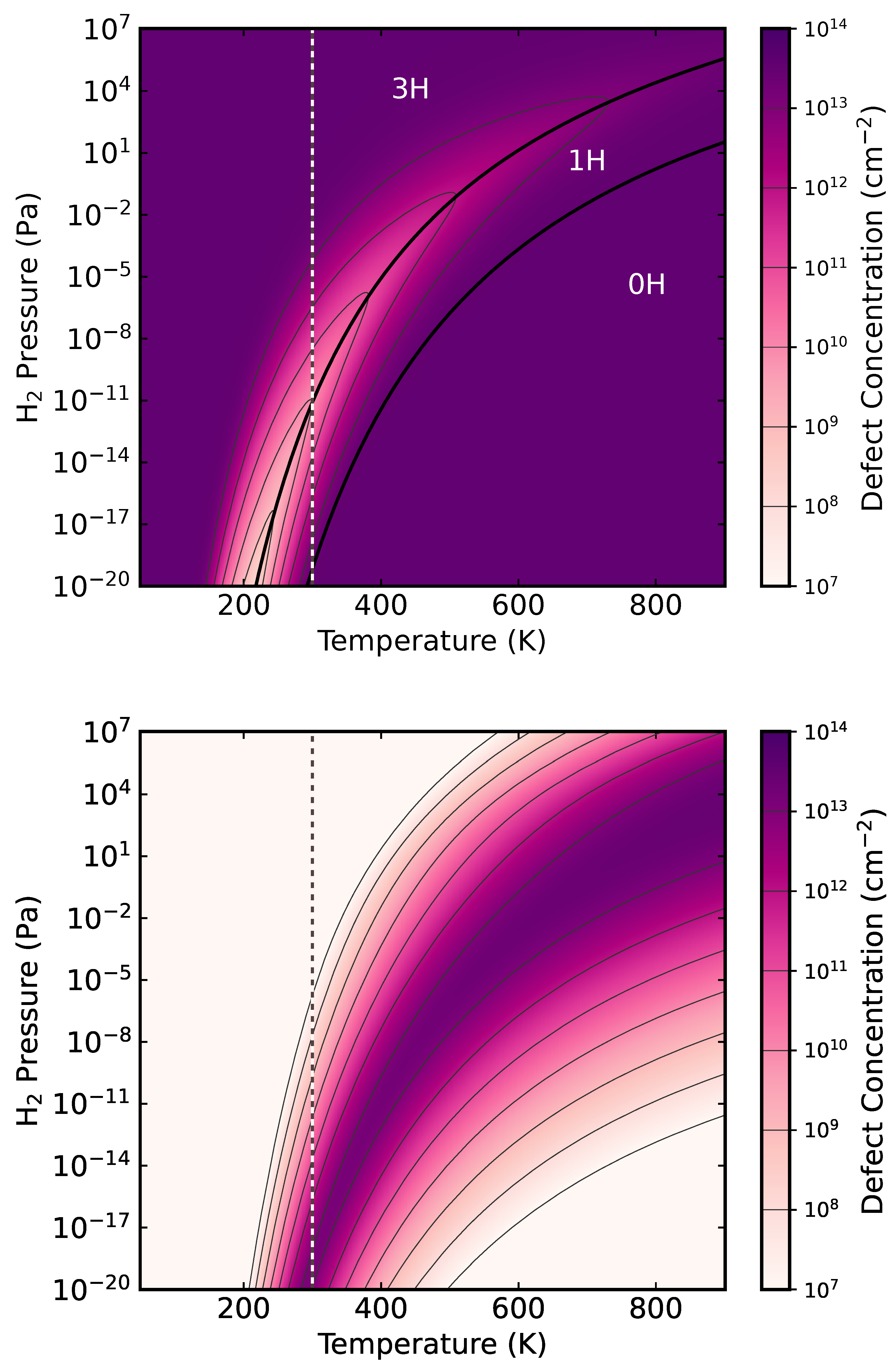
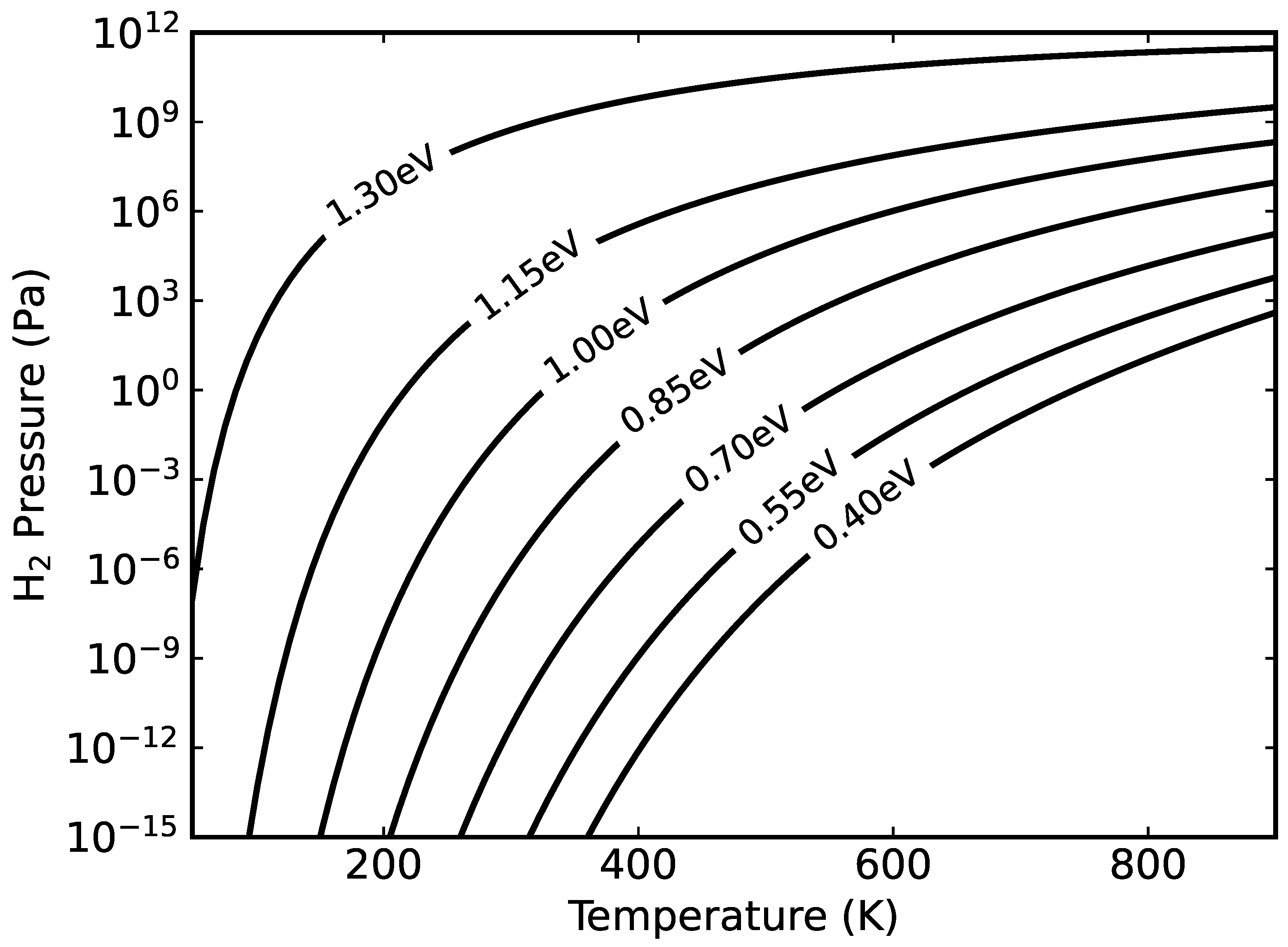
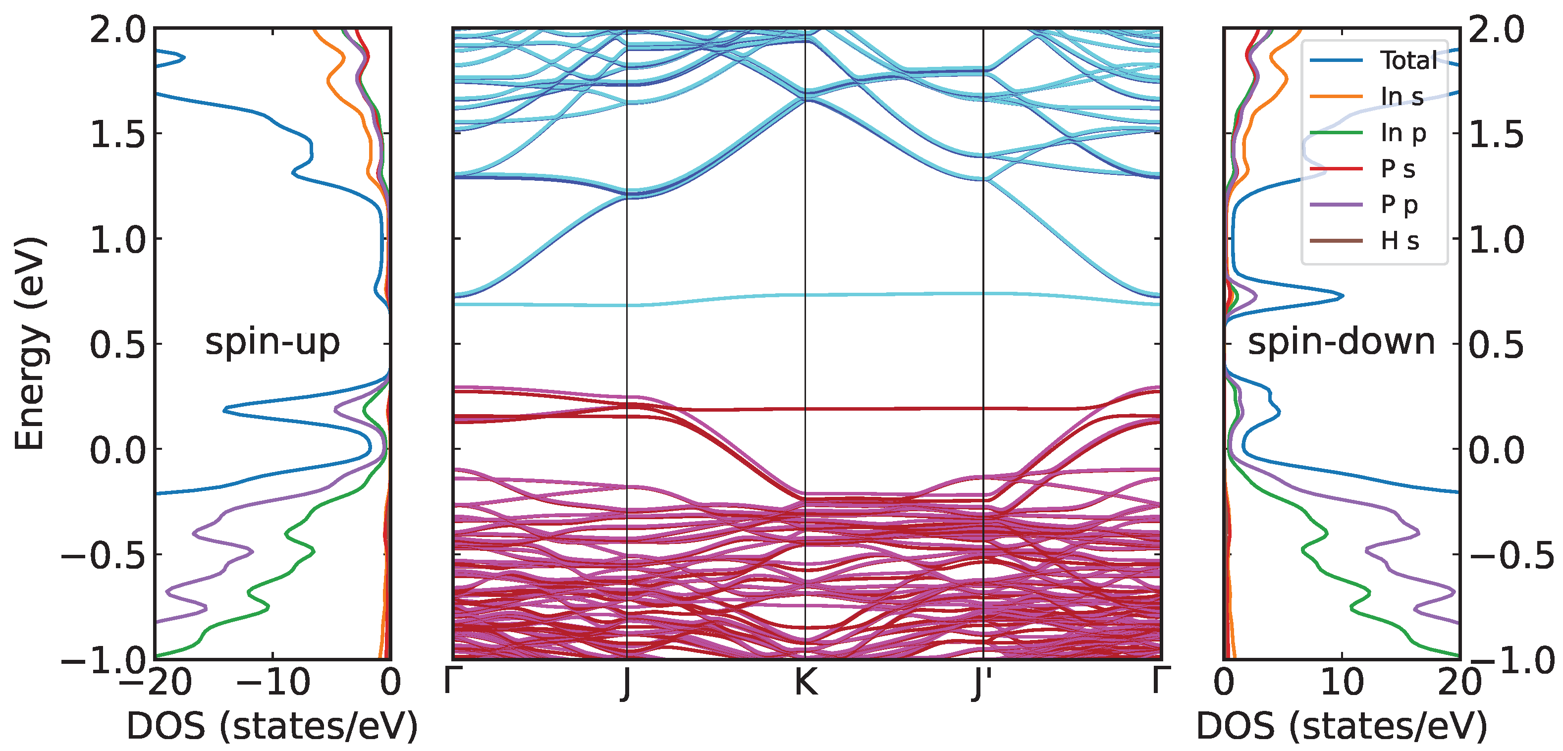
3. Results
4. Discussion
5. Conclusions
Author Contributions
Funding
Institutional Review Board Statement
Informed Consent Statement
Data Availability Statement
Conflicts of Interest
References
- Yan, Z.; Han, Y.; Lin, L.; Xue, Y.; Ma, C.; Ng, W.K.; Wong, K.S.; Lau, K.M. A monolithic InP/SOI platform for integrated photonics. Light Sci. Appl. 2021, 10, 200. [Google Scholar] [CrossRef]
- Mukherjee, C.; Deng, M.; Nodjiadjim, V.; Riet, M.; Mismer, C.; Guendouz, D.; Caillaud, C.; Bertin, H.; Vaissiere, N.; Luisier, M.; et al. Towards Monolithic Indium Phosphide (InP)-Based Electronic Photonic Technologies for beyond 5G Communication Systems. Appl. Sci. 2021, 11, 2393. [Google Scholar] [CrossRef]
- Raj, V.; dos Santos, T.S.; Rougieux, F.; Vora, K.; Lysevych, M.; Fu, L.; Mokkapati, S.; Tan, H.H.; Jagadish, C. Indium phosphide based solar cell using ultra-thin ZnO as an electron selective layer. J. Phys. D Appl. Phys. 2018, 51, 395301. [Google Scholar] [CrossRef]
- Cheng, W.H.; Richter, M.H.; May, M.M.; Ohlmann, J.; Lackner, D.; Dimroth, F.; Hannappel, T.; Atwater, H.A.; Lewerenz, H.J. Monolithic Photoelectrochemical Device for Direct Water Splitting with 19% Efficiency. ACS Energy Lett. 2018, 3, 1795–1800. [Google Scholar] [CrossRef]
- Gao, L.; Cui, Y.; Vervuurt, R.H.J.; van Dam, D.; van Veldhoven, R.P.J.; Hofmann, J.P.; Bol, A.A.; Haverkort, J.E.M.; Notten, P.H.L.; Bakkers, E.P.A.M.; et al. High-Efficiency InP-Based Photocathode for Hydrogen Production by Interface Energetics Design and Photon Management. Adv. Funct. Mater. 2016, 26, 679–686. [Google Scholar] [CrossRef]
- Schmidt, W.G. III–V compound semiconductor (001) surfaces. Appl. Phys. A 2002, 75, 89. [Google Scholar] [CrossRef]
- Pashley, M.D. Electron counting model and its application to island structures on molecular-beam epitaxy grown GaAs(001) and ZnSe(001). Phys. Rev. B 1989, 40, 10481–10487. [Google Scholar] [CrossRef]
- Schmidt, W.G.; Hahn, P.H.; Bechstedt, F.; Esser, N.; Vogt, P.; Wange, A.; Richter, W. InP(001)-(2 × 1) Surface: A Hydrogen Stabilized Structure. Phys. Rev. Lett. 2003, 90, 126101. [Google Scholar] [CrossRef]
- Chen, G.; Cheng, S.F.; Tobin, D.J.; Li, L.; Raghavachari, K.; Hicks, R.F. Indium phosphide (001)-(2 × 1): Direct evidence for a hydrogen-stabilized surface reconstruction. Phys. Rev. B 2003, 68, 121303(R). [Google Scholar] [CrossRef]
- Hannappel, T.; Visbeck, S.; Töben, L.; Willig, F. Apparatus for investigating metalorganic chemical vapor deposition-grown semiconductors with ultrahigh-vacuum based techniques. Rev. Sci. Instruments 2004, 75, 1297. [Google Scholar] [CrossRef]
- Letzig, T.; Schimper, H.-J.; Hannappel, T.; Willig, F. P-H bonds in the surface unit cell of P-rich ordered InP(001) grown by metalorganic chemical vapor deposition. Phys. Rev. B 2005, 71, 033308. [Google Scholar] [CrossRef]
- Vogt, P.; Hannappel, T.; Visbeck, S.; Knorr, K.; Esser, N.; Richter, W. Atomic surface structure of the phosphorous-terminated InP(001) grown by MOVPE. Phys. Rev. B 1999, 60, R5117. [Google Scholar] [CrossRef]
- Hahn, P.H.; Schmidt, W.G. Surface Ordering of P-rich InP(001): Hydrogen Stabilization vs Electron Correlation. Surf. Rev. Lett. 2003, 10, 163–167. [Google Scholar] [CrossRef]
- Moritz, D.C.; Ruiz Alvarado, I.A.; Zare Pour, M.A.; Paszuk, A.; Frieß, T.; Runge, E.; Hofmann, J.P.; Hannappel, T.; Schmidt, W.G.; Jaegermann, W. P-Terminated InP (001) Surfaces: Surface Band Bending and Reactivity to Water. ACS Appl. Mater. Interfaces 2022, 14, 47255–47261. [Google Scholar] [CrossRef]
- Ebert, P.; Urban, K.; Aballe, L.; Chen, C.H.; Horn, K.; Schwarz, G.; Neugebauer, J.; Scheffler, M. Symmetric Versus Nonsymmetric Structure of the Phosphorus Vacancy on InP(110). Phys. Rev. Lett. 2000, 84, 5816–5819. [Google Scholar] [CrossRef] [PubMed]
- Qian, M.C.; Göthelid, M.; Johansson, B.; Mirbt, S. Atomic and electronic properties of anion vacancies on the (110) surfaces of InP, InAs, and InSb. Phys. Rev. B 2002, 66, 155326. [Google Scholar] [CrossRef]
- Hedström, M.; Schindlmayr, A.; Schwarz, G.; Scheffler, M. Quasiparticle Corrections to the Electronic Properties of Anion Vacancies at GaAs(110) and InP(110). Phys. Rev. Lett. 2006, 97, 226401. [Google Scholar] [CrossRef]
- Rosenzweig, D.S.; Hansemann, M.N.L.; Schnedler, M.; Ebert, P.; Eisele, H. Atomically resolved study of initial stages of hydrogen etching and adsorption on GaAs(110). Phys. Rev. Mater. 2022, 6, 124603. [Google Scholar] [CrossRef]
- Rosenzweig, D.S.; Schnedler, M.; Dunin-Borkowski, R.E.; Ebert, P.; Eisele, H. Morphologic and electronic changes induced by thermally supported hydrogen cleaning of GaAs (110) facets. J. Vac. Sci. Technol. B 2023, 41, 044202. [Google Scholar] [CrossRef]
- Kresse, G.; Furthmüller, J. Efficiency of ab-initio total energy calculations for metals and semiconductors using a plane-wave basis set. Comp. Mat. Sci. 1996, 6, 15–50. [Google Scholar] [CrossRef]
- Perdew, J.P.; Burke, K.; Ernzerhof, M. Generalized Gradient Approximation Made Simple. Phys. Rev. Lett. 1996, 77, 3865–3868. [Google Scholar] [CrossRef] [PubMed]
- Krukau, A.V.; Vydrov, O.A.; Izmaylov, A.F.; Scuseria, G.E. Influence of the Exchange Screening Parameter on the Performance of Screened Hybrid Functionals. J. Chem. Phys. 2006, 125, 224106. [Google Scholar] [CrossRef] [PubMed]
- Blöchl, P.E. Projector augmented-wave method. Phys. Rev. B 1994, 50, 17953–17979. [Google Scholar] [CrossRef]
- Kresse, G.; Joubert, D. From ultrasoft pseudopotentials to the projector augmented-wave method. Phys. Rev. B 1999, 59, 1758–1775. [Google Scholar] [CrossRef]
- Freysoldt, C.; Grabowski, B.; Hickel, T.; Neugebauer, J.; Kresse, G.; Janotti, A.; Van de Walle, C.G. First-principles calculations for point defects in solids. Rev. Mod. Phys. 2014, 86, 253–305. [Google Scholar] [CrossRef]
- Valtiner, M.; Todorova, M.; Grundmeier, G.; Neugebauer, J. Temperature Stabilized Surface Reconstructions at Polar ZnO(0001). Phys. Rev. Lett. 2009, 103, 065502(R). [Google Scholar] [CrossRef]
- Zhang, X.; Grabowski, B.; Körmann, F.; Freysoldt, C.; Neugebauer, J. Accurate electronic free energies of the 3d,4d, and 5d transition metals at high temperatures. Phys. Rev. B 2017, 95, 165126. [Google Scholar] [CrossRef]
- Janak, J.F. Proof that = ϵ in density-functional theory. Phys. Rev. B 1978, 18, 7165–7168. [Google Scholar] [CrossRef]
- Sanna, S.; Frauenheim, T.; Gerstmann, U. Validity of the Slater-Janak transition-state model within the LDA+U approach. Phys. Rev. B 2008, 78, 085201. [Google Scholar] [CrossRef]
- Gallino, F.; Pacchioni, G.; Di Valentin, C. Transition levels of defect centers in ZnO by hybrid functionals and localized basis set approach. J. Chem. Phys. 2010, 133, 144512. [Google Scholar] [CrossRef]
- Madelung, O. Semiconductors: Group IV Elements and III-V Compounds (Data in Science and Technology); Springer: Berlin, Germany, 2013. [Google Scholar]
- Kim, Y.S.; Hummer, K.; Kresse, G. Accurate band structures and effective masses for InP, InAs, and InSb using hybrid functionals. Phys. Rev. B 2009, 80, 035203. [Google Scholar] [CrossRef]
- Schmidt, W.G.; Esser, N.; Frisch, A.M.; Vogt, P.; Bernholc, J.; Bechstedt, F.; Zorn, M.; Hannappel, T.; Visbeck, S.; Willig, F.; et al. Understanding reflectance anisotropy: Surface-state signatures and bulk-related features in the optical spectrum of InP(001)(2 × 4). Phys. Rev. B 2000, 61, R16335. [Google Scholar] [CrossRef]
- Chantis, A.N.; van Schilfgaarde, M.; Kotani, T. Ab Initio Prediction of Conduction Band Spin Splitting in Zinc Blende Semiconductors. Phys. Rev. B 2006, 96, 086405. [Google Scholar] [CrossRef]
- Hannappel, T.; Töben, L.; Möller, K.; Willig, F. In-Situ Monitoring of InP(100) and GaP(100) Interfaces and Characterization with RDS at 20 K. J. Electron. Mater. 2001, 30, 1425. [Google Scholar] [CrossRef]


Disclaimer/Publisher’s Note: The statements, opinions and data contained in all publications are solely those of the individual author(s) and contributor(s) and not of MDPI and/or the editor(s). MDPI and/or the editor(s) disclaim responsibility for any injury to people or property resulting from any ideas, methods, instructions or products referred to in the content. |
© 2024 by the authors. Licensee MDPI, Basel, Switzerland. This article is an open access article distributed under the terms and conditions of the Creative Commons Attribution (CC BY) license (https://creativecommons.org/licenses/by/4.0/).
Share and Cite
Sciotto, R.; Ruiz Alvarado, I.A.; Schmidt, W.G. Substrate Doping and Defect Influence on P-Rich InP(001):H Surface Properties. Surfaces 2024, 7, 79-87. https://doi.org/10.3390/surfaces7010006
Sciotto R, Ruiz Alvarado IA, Schmidt WG. Substrate Doping and Defect Influence on P-Rich InP(001):H Surface Properties. Surfaces. 2024; 7(1):79-87. https://doi.org/10.3390/surfaces7010006
Chicago/Turabian StyleSciotto, Rachele, Isaac Azahel Ruiz Alvarado, and Wolf Gero Schmidt. 2024. "Substrate Doping and Defect Influence on P-Rich InP(001):H Surface Properties" Surfaces 7, no. 1: 79-87. https://doi.org/10.3390/surfaces7010006
APA StyleSciotto, R., Ruiz Alvarado, I. A., & Schmidt, W. G. (2024). Substrate Doping and Defect Influence on P-Rich InP(001):H Surface Properties. Surfaces, 7(1), 79-87. https://doi.org/10.3390/surfaces7010006