Article

The Effects of Substrate Temperature on the Growth, Microstructural and Magnetic Properties of Gadolinium-Containing Films on Aluminum Nitride

by
Craig A. Ekstrum
1,
Ragavendran Venkatesan
2,
Chito Kendrick
1,
Moshe Einav
1,
Paramasivam Sivaprakash
3,
Jeyanthinath Mayandi
2,*,
Sonachalam Arumugam
3 and
Joshua M. Pearce
4,*
1
Department of Materials Science & Engineering, Michigan Technological University, Houghton, MI 49931, USA
2
Department of Materials Science, School of Chemistry, Madurai Kamaraj University, Madurai 625021, India
3
Center for High and Ressure Research, School of Physics, Bharathidasan University, Tiruchirappalli 620024, India
4
Department of Electrical & Computer Engineering, Ivey Business School, Western University, 1151 Richmond St. N., London, ON N6A 3K7, Canada
*
Authors to whom correspondence should be addressed.
Surfaces 2022, 5(2), 321-333; https://doi.org/10.3390/surfaces5020024
Submission received: 8 March 2022 / Revised: 4 June 2022 / Accepted: 6 June 2022 / Published: 9 June 2022
(This article belongs to the Collection Featured Articles for Surfaces)

Abstract

:
To facilitate future novel devices incorporating rare earth metal films and III-V semiconductors on Si substrates, this study investigates the mechanisms of growth via molecular beam epitaxy of gadolinium (Gd) on aluminum nitride (AlN) by determining the impact of substrate temperature on microstructure. The Gd films underwent extensive surface analysis via in situ reflective high energy electron diffraction (RHEED) and ex-situ SEM and AFM. Characterization of the surface features of rare earth metal films is important, as surface geometry has been shown to strongly impact magnetic properties. SEM and AFM imaging determined that Gd films grown on AlN (0001) from 80 °C to 400 °C transition from wetting, nodular films to island–trench growth mode to reduce in-plane lattice strain. XRD and Raman spectroscopy of the films revealed that they were primarily comprised of GdN, Gd and Gd2O3. The samples were also analyzed by a vibrating sample magnetometer (VSM) at room temperature. From the room temperature magnetic studies, the thick films showed superparamagnetic behavior, with samples grown between 240 °C and 270 °C showing high magnetic susceptibility. Increasing GdN (111) 2θ peak position and single-crystal growth modes correlated with increasing peak magnetization of the thin films, suggesting that lattice strain in single-crystal films was the primary driver of enhanced magnetic susceptibility.

1. Introduction

Gadolinium (Gd) is a ferromagnetic material with a bulk Curie temperature (TC) of 293 K, which is the highest TC of the rare earth metals. Of additional interest is the ability to further increase the Tc of Gd by altering crystalline morphology and strain in thin films. Given that the magnetic heating and cooling of a material is greatest near its TC, Gd has interesting applications of its magnetocaloric effect, which occurs strongest near the temperature of many worldly processes such as magnetic heating, refrigeration and sensing. Thin films of Gd have been shown to have enhanced magnetocaloric effect [1,2], and Gd thick films for energy conversion applications are a current area of research [3] providing additional research interest in the magnetic properties of Gd films.
The nitride of Gd is also of interest to magnetocaloric and semiconductor devices. GdN is a semiconducting ferromagnetic material, which has potential applications in semiconductor and spintronics devices. Khazen et al. [4] prepared two types of gadolinium nitride (GdN) thin films by thermal evaporation of Gd in an N2 atmosphere and by ion beam assisted deposition with a typical thickness of 200 nm deposited on (100) oriented Si substrates at room temperature. Natali et al. [5] have grown epitaxial films of the ferromagnetic semiconductor GdN on Si (111), preventing problematic silicide formation with a wurtzite (0001) AlN buffer layer. This paves the way for the future integration of this intrinsic ferromagnetic semiconductor on silicon that has potential roles in spintronics.
There has also been considerable debate on the nature of the TC of Gd. Michels et al. [6] experimentally studied the dependence of TC on the average crystallite size of nanostructured Gd prepared by the inert-gas condensation method. Measurements of heat capacity and AC magnetic susceptibility indicate that TC shifts to lower temperatures and the Curie transition takes on an increasingly broadened and rounded appearance with decreasing crystallite size. The latter was inconsistent with the finite-size effect observed in Gd films. Rather, the shift in Tc could best be understood as a consequence of the significant internal pressure induced by the interface stress of high-angle grain boundaries in Gd. For example, Gd films have been found to have an enhanced TC up to 315 K when grown on W (110) [7]. Other studies have reported that the surface of Gd films can exhibit an extraordinary transition with a separate high TC relative to the bulk Tc (ranging from 288 K to 358 K) [8,9,10,11,12,13,14,15,16,17,18], while other studies [19,20,21,22,23,24,25,26] indicate the surface transition is only ordinary with identical surface and bulk TC. The Gd surface has been classified experimentally as an ordinary 3-D Heisenberg ferromagnet and showed conclusively that the surface and bulk have the same TC [27]. The debate lasted for nearly two decades because of the experimental challenges of preparing structurally and magnetically ordered Gd surfaces, which demanded ultrahigh vacuum evaporation on a lattice-matched substrate.
Three primary methods have found to be successful for studying magnetic properties of crystalline Gd films. These are: (1) deposition on W (110) at room temperature with a subsequent anneal between 420–875 K [19,23,27]; (2) deposition on Y (0001) single crystals at high temperature with an anneal [25]; and (3) deposition between relatively inert metallic films followed by an anneal between 420–875 K, for which Ta films have been used [2], as have Cr [27]. The W, Ta and Cr-substrate methods provide substrates which do not readily alloy with Gd. Growth on W (110) substrates causes signification lattice strain at the atomic interface, which causes differences between surface and bulk properties, while growth on Y (0001) substrates results in an unstrained Gd. Growth on sputtered Ta substrates has required subsequent annealing of the deposited Gd films to achieve high magnetization, as amorphous deposition is leveraged to keep the underlying film smooth [2]. These methods rely on expensive and relatively rare substrates, which limit the applications of Gd films grown on them, while also typically requiring subsequent annealing steps to increase the magnetization of the film. In addition, many of the studies involving Gd films have only characterized thin films in the order of a few to several monolayers [7,8,28,29], with others not characterizing films beyond tens of nanometers [2,27].
Strain relief in Gd films grown on lattice-strained substrates such as W (110) has been found to drive film morphology and impact the magnetic susceptibility of films. At ambient temperatures, Gd films deposited on W (110) have been found to deposit in layer-by-layer growth [30,31,32]. However, deposition of Gd on W (110) at elevated temperatures (723 K and 773 K) has shown that films exhibit Stranski–Krastanov growth morphology (island structure), indicating film strain relief as impacting growth morphology [7]. Tober et al. [7] and Farle et al. [31,32] have also shown that annealing Gd thin films grown at room temperature causes a transition from a two-dimensional structure to a 3-D island system atop a few monolayers. These studies have shown that the development of 3-D islands reduces the TC towards bulk [31,32], and reduces the magnetic susceptibility of the films after the structural transition to island structures during the anneal at high temperature (near 700 K) [7,31,32]. More recently, however, multiple studies have reported annealing to increase the magnetic susceptibility of Gd films at annealing temperatures up to 875 K [2,27].
The magnetic behavior of thick films (>100 nm) of Gd on lattice-mismatched substrates has not been widely studied. Additionally, given that much of the literature focuses on room-temperature or elevated-temperature deposition of Gd films, there is a gap in understanding Gd film structural development as growth temperature is gradually increased. Strain in Gd films impacts the growth regime, which ultimately impacts magnetic characteristics. Therefore, understanding the mechanisms by which Gd films develop their morphologies on different substrates and under different growth temperatures in the thicker regimes (>100 nm) is important.
To overcome these limitations, this study investigates thick Gd films (~200 nm) grown by molecular beam epitaxy (MBE) on a relatively inexpensive and common substrate of aluminum nitride (AlN) (0001). Growth of these films was performed over a range of temperatures from 80 to 400 °C. The Gd films underwent extensive surface analysis in situ reflective high energy electron diffraction (RHEED) and ex-situ SEM and AFM as the characterization of surface features are important for magnetic properties of rare earth metal films, which are strongly affected by surface geometry [7,29].

2. Materials and Methods

The Gd films were grown in an ISA Riber 32 MBE system (Riber, Santa Barbara, CA, USA), with base pressures in the 10−9 Torr range. Growth temperatures were at 80 °C, 210 °C, 240 °C, 255 °C, 270 °C, 330 °C and 400 °C. Films were grown on 2-inch Si (111) wafers coated with 230 nm AlN (0001), which had been preprocessed by MTI Corporation (Richmond, CA, USA). The Si/AlN wafers were cleaned ultrasonically in acetone, then methanol, followed by a deionized water ultrasonic rinse. After drying the clean wafers with compressed N2, they were mounted on graphite plates and transferred into a load lock chamber and subsequently the growth chamber after pressures equalized within 10−3 Torr. During deposition, wafers were heated from the rear with radiative W heating elements, with the graphite plates providing improved thermal homogeneity. Thermal uniformity was also improved by constant rotation of the substrates during growth. Substrate temperature was monitored by a thermocouple contacting the back of the graphite plates at the center of the samples. It should be noted that a thermal gradient existed from center to edge of the wafers; this effect was minimized by characterizing the films near the center of the wafer, to reduce growth temperature error relative to thermocouple measurements.
The substrates were outgassed at 800 °C before each growth. Gd fluxes were introduced to the substrate from a Knudsen effusion cell centered on the rotating substrate. Effusion rates were measured with a quartz crystal rate monitor. The depositions were timed to allow the ideal thickness of 200 nm, except for the 255 °C sample, which was timed to produce a film 400 nm thick, assuming the Gd source rate held at 1 Å/s. Fluxes centered at 1 Å/s, with a variance of +/− 0.05 Å/s. During each growth, the rate dropped approximately 0.1 Å/s by the growth’s completion. It can be noted in Figure 1h that the thicknesses of the 330 °C sample is indeed less than the target thickness of 200 nm. The 330 °C thickness (150 nm) is representative of the thickness of samples grown at other temperatures except for 255 °C (thickness of 300 nm) and 400 °C (thickness of 200–210 nm). Higher film thickness at 255 °C is due to this sample being deposited for twice as long as other lower-temperature samples, and higher thickness at 400 °C is due to island–trench formation causing a difference in film thickness. Thermal history of the 255 °C sample was also distinct from the others in that it was annealed at its growth temperature for 30 min after film deposition was completed. Different thermal history was imparted on this sample to study the effect of annealing on magnetic susceptibility of the sample, as annealing has been a common method in the literature for enhancing magnetic properties [7,31,32]. This was achieved by shielding the Gd effusion cell from the sample and maintaining 255 °C while the sample was rotated for 30 min. After growth, all samples were allowed to cool to below 100 °C before transfer to the higher-vacuum load lock cell.
The samples were imaged with a Hitachi S-4700 FE-SEM (Schaumburg, IL, USA) at 15 kV in secondary electron imaging mode and a Veeco Dimension 3000 AFM (Plainview, NY, USA) in tapping mode. X-ray diffraction (XRD) data was collected with a Scintag XDS-2000 (Cupertino, CA, USA) containing a Cu target, which produced x-rays with a wavelength of 1.5406 Å). Films were monitored in situ with a kSA 400 RHEED system (Dexter, MI, USA), and images were captured with a CCD camera at the end of film growth. Raman-scattering measurements were performed in 180° backscattering geometry using a LabRamHR800 Spectrometer from Horiba Jobin–Yvon (Kyoto, Japan) equipped with a CCD detector. The samples were excited by 633 nm emission from a He–Ne laser and the resolution of the spectrometer used was about 0.3 cm−1. Field-dependent magnetization measurements were taken in up to a 60 K Oe field using the Vibrating Sample magnetometer (VSM) option of the Physical property Measuring System (Model: 6000, Quantum Design, San Diego, CA, USA). During VSM measurements, films were oriented such that vibration was perpendicular to the uniform magnetic field (film thickness dimension parallel to magnetic field orientation).

3. Results and Discussion
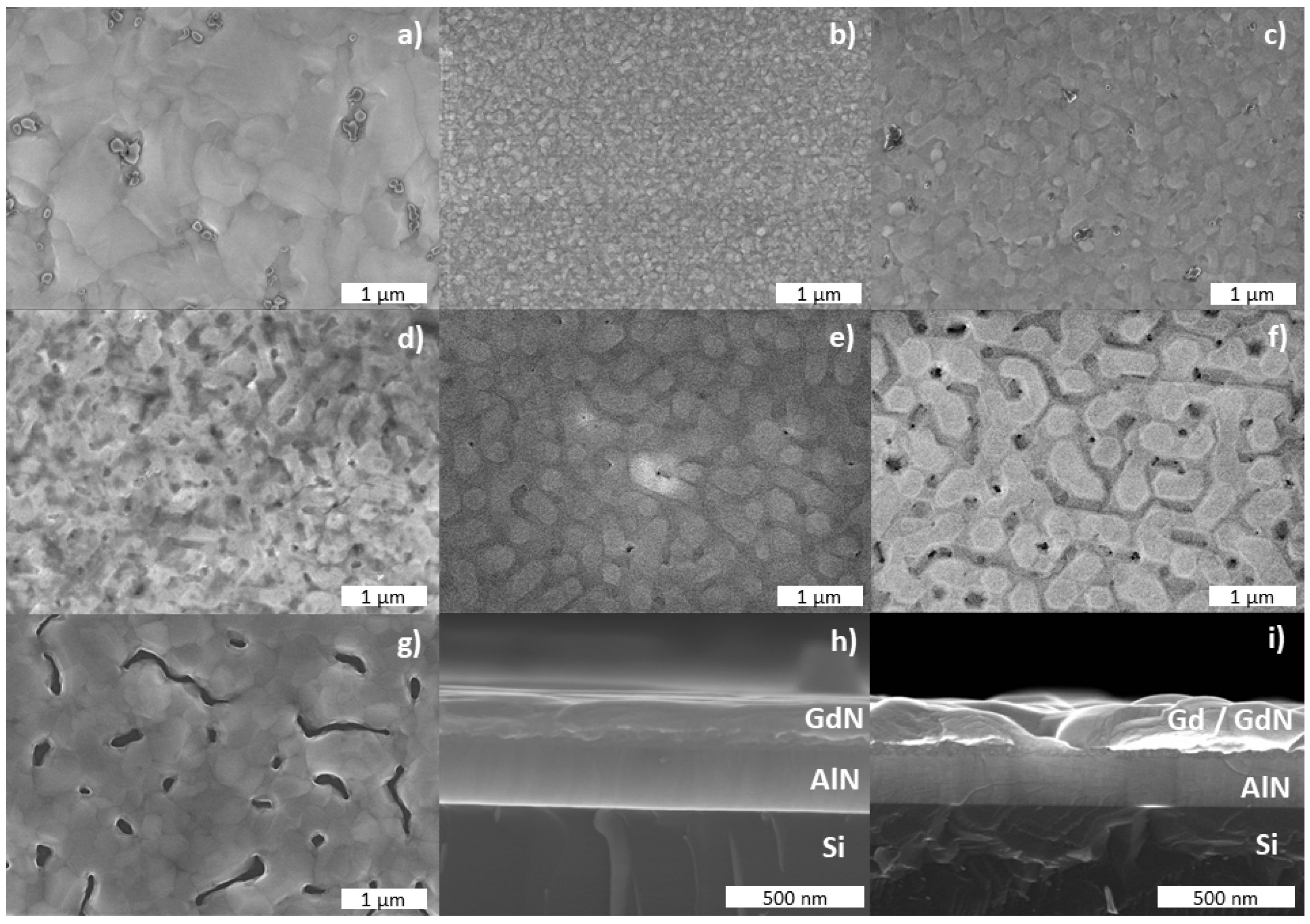
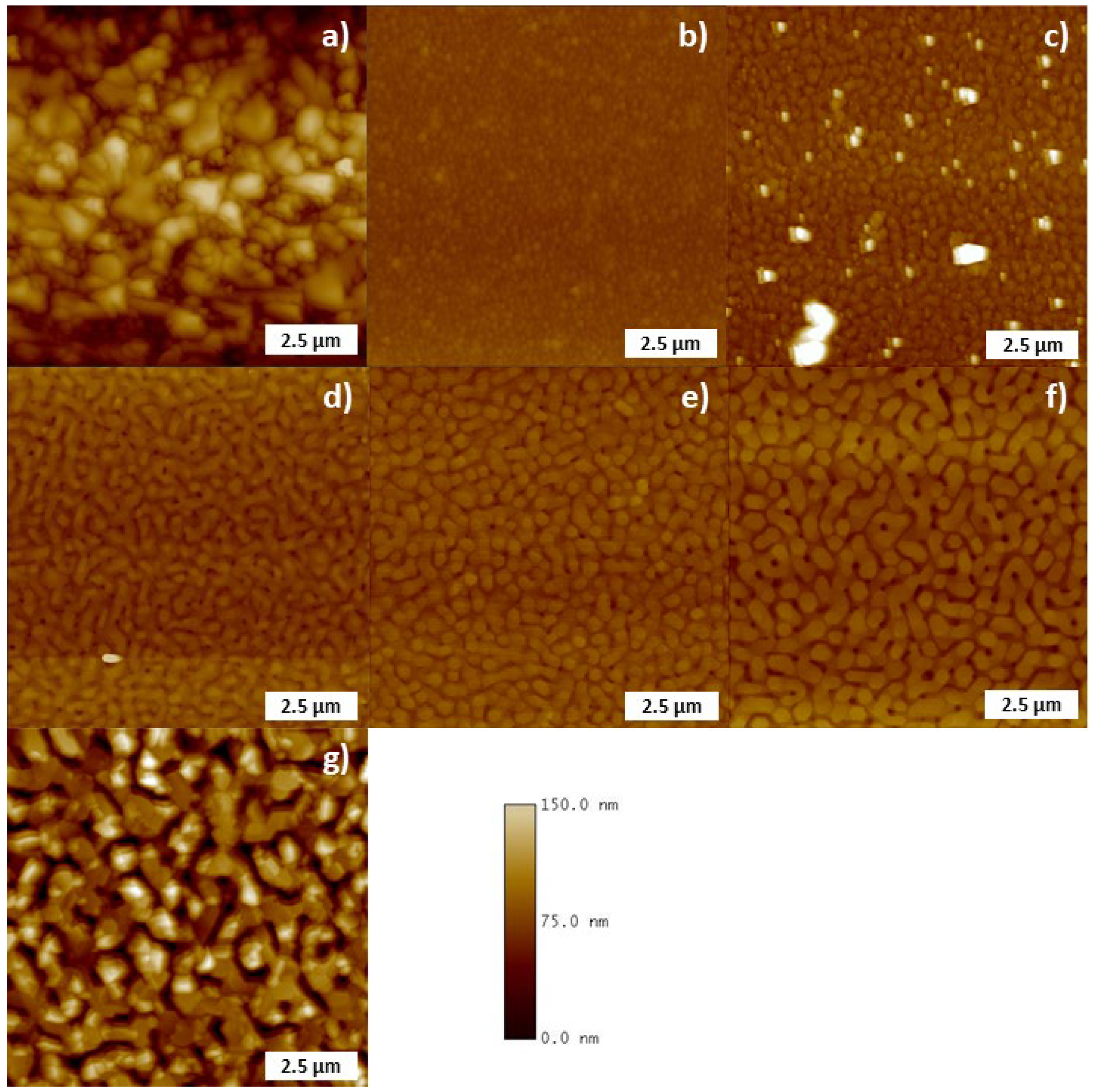
3.1. SEM and AFM

Secondary electron imaging of the Gd films shows that film morphology changes with deposition temperature (Figure 1). Growth at 80 °C results in a nodular film (Figure 1a). An increase in growth temperature resulted in the formation of fine grains (210 °C, Figure 1b), followed by segregation into hexagonal island chains with trenches separating them (240 °C to 330 °C, Figure 1c–f). By 400 °C, the island chains become very coarse, with deep trenches (Figure 1g). Another trend with growth temperature is island width. Film morphology becomes morphologically similar to the Stranski–Krastanov growth mode (a few smooth monolayers with 3-D island growth after a critical thickness) which has been proposed by Weller as the primary growth mode of Gd thin films on W (110), at a growth temperature of 450 °C [8].
AFM imaging revealed very similar morphological development as the secondary electron SEM imaging, with nodular films progressing to hexagonal island–trench systems with increasing growth temperature (Figure 2). AFM also revealed increasing trench depth with temperature (increasing from 255 °C to 400 °C). Additionally, AFM imaging highlighted very fine hexagonal particles on the surface of the island–trench film structure at 255 °C (Figure 2d); these structures were not visible in the secondary SEM.
Similar Gd film morphology appears to develop for Gd films grown at 400 °C on AlN (0001), which has a 16.7% lattice mismatch with Gd, as for Gd films grown on W (110) substrates, on which Gd growth is also highly strained (approximately 14.9%, according to Weller and Alvarado) [8]. This suggests that surface behavior is strongly dependent on both strain state and growth temperature, in both homosymmetrical and heterosymmetrical systems.
There is an especially large difference between the 330 °C and 400 °C as compared to the evolution of the other samples’ microstructures (Figure 1h,i). The 400 °C sample has a thin layer of growth followed by large hills. The 330 °C sample showed slighter hills and a thicker film below the hills (Figure 1h,i). This shows a transition towards island–trench growth that is reminiscent of the Stranski–Krastanov-like growth observed for Gd films on W (110) by Tober et al. [7]. This is also exemplified by the 300 °C and 400 °C AFM images (Figure 2f,g). Comparison between the Gd on AlN (0001) system and the Gd on W (110) system as proposed by Weller is possible, for film thickness up to 100 nm was investigated, which approaches the thickness of those films considered in this study. With this in mind, the magnetic properties of the 400 °C sample may be similar to those prepared in [7].

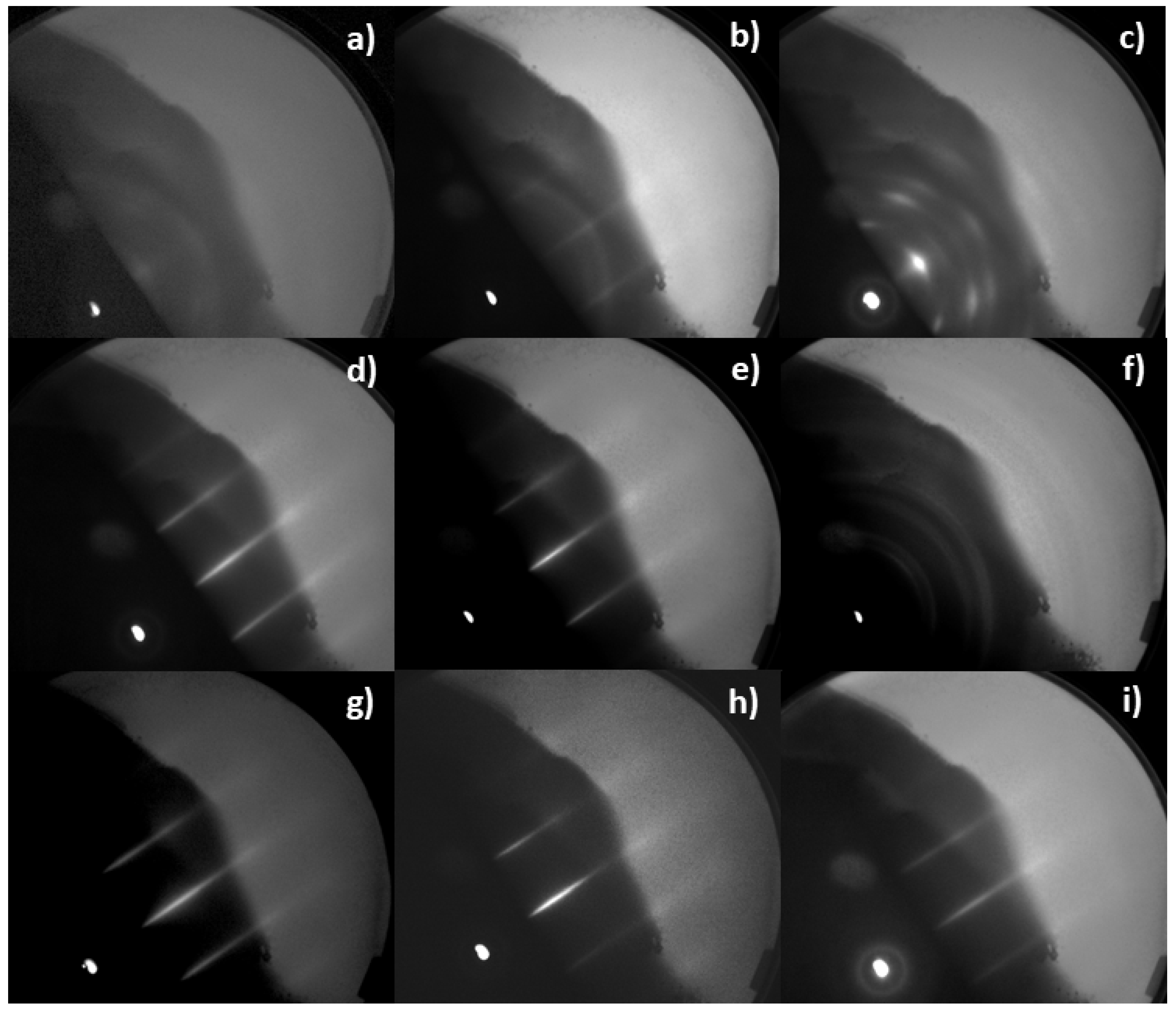
3.2. In Situ RHEED Measurements

The RHEED images (Figure 3) show the development of crystallinity through the temperature series. RHEED of films grown at 80 °C showed weak rings, indicating a partially polycrystalline, but otherwise amorphous film. The 210 °C sample RHEED shows faint rings, streaks and spots, indicating an oriented polycrystalline film. All other samples, however, exhibit streaks only, indicating single-crystalline Gd films growing in a layer-by-layer Frank–van der Merwe regime [33,34]. It is interesting to note that the development of the island–trench morphology, while morphologically similar to Stranski–Krastanov growth, is likely distinct given that RHEED data supports layer-by-layer growth. The 255 °C-annealed RHEED image shows rings, indicating the film surface converted to a polycrystalline structure. This degradation of the film’s crystallinity suggests that the Gd grew at 255 °C, and potentially other temperatures, is metastable. It should be noted that the 255 °C sample was converted to a polycrystalline film through annealing at its growth temperature for 30 min, as indicated by the RHEED images, Figure 3e,f. Even so, the SEM and AFM images still reflect the island–trench morphology.

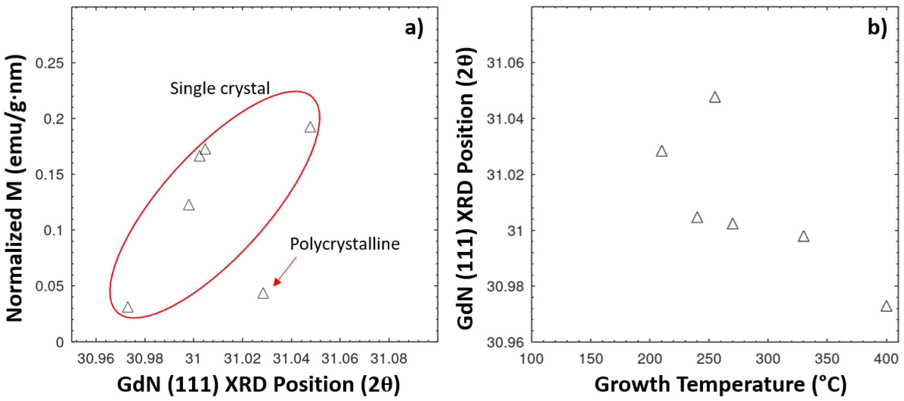
3.3. XRD Pattern Analysis

XRD diffraction patterns for Gd/AIN/Si prepared under various temperatures showed multiple Gd-bearing phases were present in the films (Figure 4b). A key learning from XRD measurements was that the deposited films are primarily comprised of GdN, Gd2O3 and Gd. Strong diffraction peaks at 28.46° are attributed to Si (111) [JCPDS card file No: 80-0018]. The other strong peak at 36.14° and 76.63° corresponds with AlN (0002) and (0004) planes (Figure 4a). Both the Si and AlN peaks exhibit shoulders, which are present due to Cu Kβ diffraction peaks. The peak observed at 32.43° is ascribed to Gd (101) [JCPDS card file No: 002-0864] and the other peaks appeared at 28.42° (222), 29.18° (401) and 33.27° (400) to Gd2O3 [JCPDS card file No: 011-0604 and 012-0474]. It is possible that overlap of the Si (111) and (222) Gd2O3 peaks hid the presence of Gd2O3 in the 240 °C and 270 °C samples. Further diffraction peaks at 30.97° (111) and 64.51° (222) are associated with GdN [JCPDS card file No: 015-0888].
XRD data also provides information on the structure of the 80 °C and 250 °C films. The 80 °C film showed diffraction peaks attributable to the substrate materials and very weak peaks at 25.68°, 27.24°, 32.1° (GdN (111), [JCPDS card file No: 015-0888]) and 37.76°. This indicates that while the Gd film contains some crystalline phases, the film is primarily amorphous, which corroborates the RHEED pattern from growth. That the 255 °C sample XRD showing only peaks for GdN (111) supports the theory that the film, although RHEED showed a polycrystalline surface after annealing, is still extremely oriented.
The XRD spectra of all samples showed AlN (0002) and (0004) diffraction peaks, and films grown at 240 °C and 270 °C showed Si (111) peaks. All films show the presence of GdN (111), indicating that solid-state diffusion between the AlN and Gd occurred during deposition, converting at least some of the film into GdN. Peaks indicating Gd (101) and Gd2O3 (222), (401) and (400) were observed for films grown at 210 °C and 400 °C; the correlation of Gd and Gd2O3 indicates substantial Gd oxidation where un-nitrided Gd films were present.
GdN (111) diffraction peak position data suggests that the development of the island–trench system is a form of strain relief for the Gd layer. This is indicated by the trend of increasing growth temperature with the GdN (111) 2θ position converging on the un-strained value of 30.97° (this value from JCPDS card file No: 015-0888). The one sample that deviates from this is 255 °C, which has a higher GdN (111) 2θ than any other sample.
The GdN (111) d spacing, lattice constants, crystallite size, and net lattice distortion of the samples were estimated using formulas in Ref. [35] and are displayed in Table 1. Crystallite size was found to increase with growth temperature from 210 °C to 255 °C, where the crystallite size stabilized at an average of 54 from 255 °C to 400 °C. The estimated error of the crystallite size calculations was on the order of ± 3 nm for each growth temperature, which means that crystallite size from 255 °C to 400 °C is likely very similar, and within measurement error. Similar crystallite sizes in this temperature range were noted only on samples exhibiting clear island–trench morphology, indicating that the crystallite size may be dependent on film growth mode.

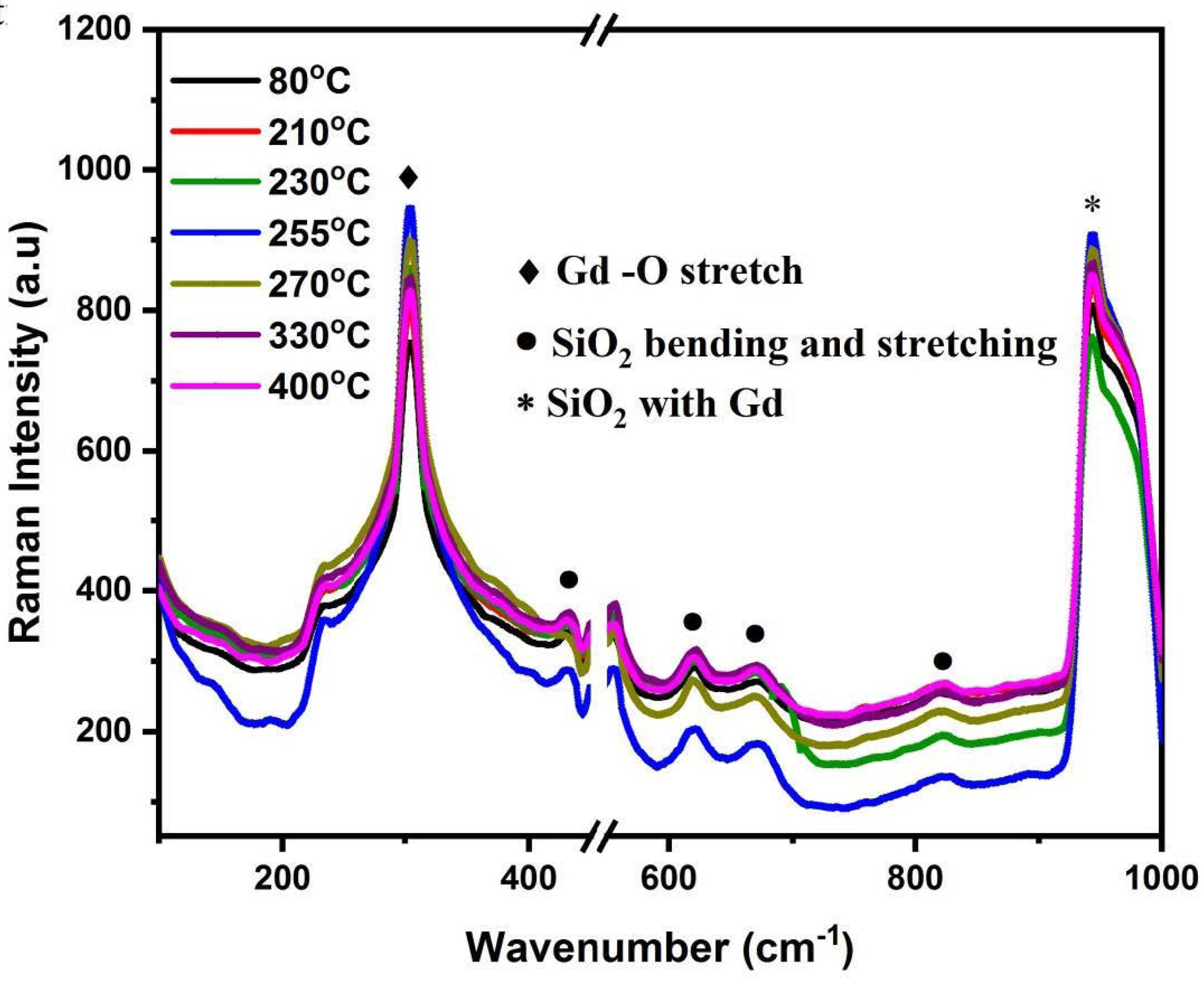
3.4. Raman Spectroscopy Analysis

Raman spectra showed peaks at 230, 307, 434, 620, 670, 819 and 942 cm−1 (Figure 5). The plot of spectra for the films has a break from 450 cm−1 to 550 cm−1 to avoid the strong Raman peak from the Si substrate, which suppresses the intensity of other peaks. The strong peak at 307 cm−1 has been assigned as Gd–O stretching, which is attributed to the formation of Gd2O3 [36]. Given that samples were not passivated, Gd at the film surface would have likely been oxidized to form Gd2O3. Given the lack of strong Gd peaks from XRD measurements, it is likely that the Gd was either converted into the nitride by solid-state diffusion during deposition or oxidized into Gd2O3 during exposure to the atmosphere between growth and both Raman and VSM measurements. Gd2O3 is paramagnetic at room temperature, with a low peak magnetization on the order of single-digit emu/g [37,38]. Gd2O3 content in Gd films has been shown to reduce film susceptibility [2], which suggests that the presence of Gd2O3 in the samples grown in this study limited the maximum magnetization. The peak at 942 cm−1 has been assigned to the combination of SiO2 with Gd [39]. The peaks at 434, 620, 670 and 819 cm−1 are SiO2 bending and stretching modes.
All the peaks are in good agreement with those reported in the literature [40], which provides strong evidence that all samples contain both Gd and Gd2O3; this compliments the XRD measurements of the films, which showed a strong preference for GdN. The compiled XRD and Raman characterization suggests that the films have the following structure: Si/AlN/GdN/Gd/Gd2O3, with the GdN film being the thickest of the deposited layers.

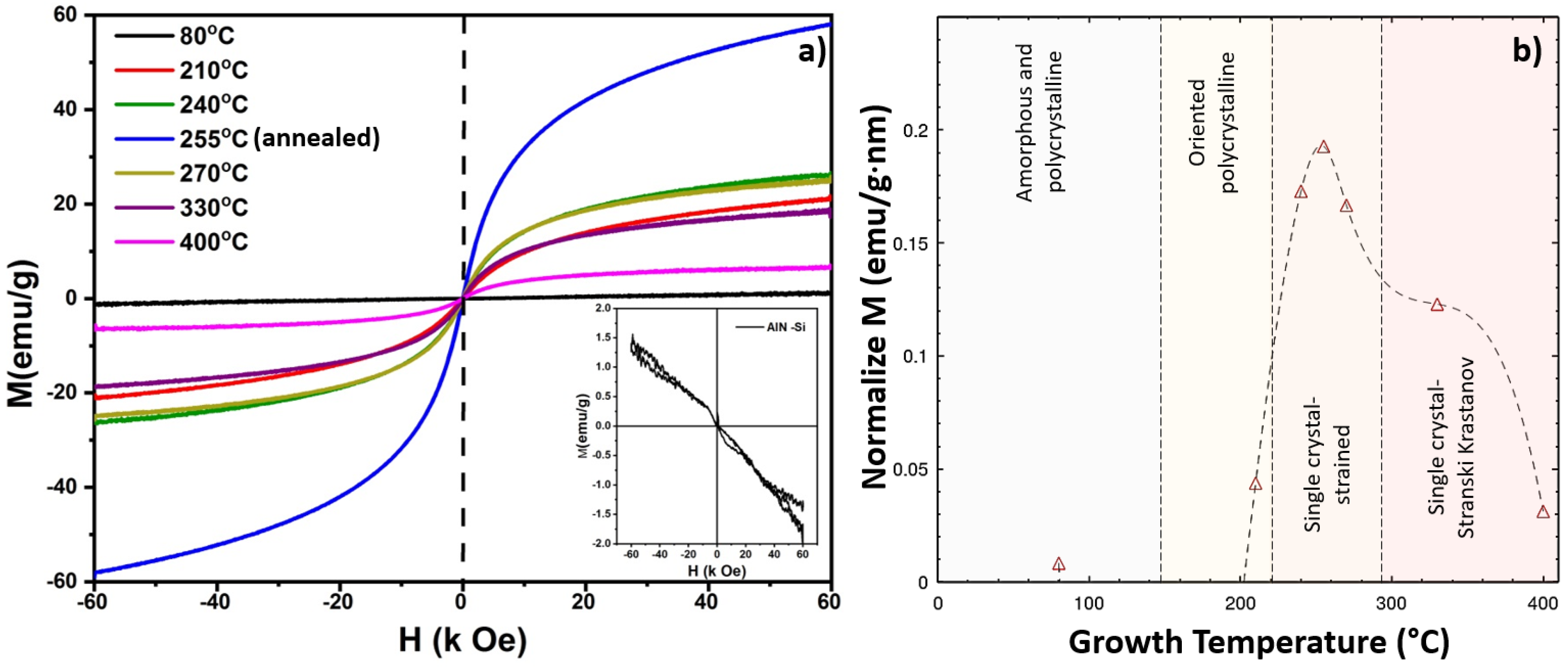
3.5. Isothermal Magnetic Properties

Field-dependent magnetization curves varied drastically with growth temperature of the GdN/Gd/Gd2O3 films (Figure 6). The magnetization of the films showed an S–type behavior, except for the 80 °C film which exhibited weak linear paramagnetism. Magnetization curves had a similar nature to the Langevin function [36]. The inset in the figure shows the perfect diamagnetism of the substrate AlN/Si. When increasing the field, magnetization was increased up to 60 K Oe, and no hysteresis loop was observed, revealing that the films grown at 210 °C to 400 °C exhibited superparamagnetic behavior. The annealed sample (255 °C growth temperature) showed a slightly higher thickness-normalized magnetic saturation relative to the 240 °C and 270 °C films (Figure 6b).
Film growth mode and lattice strain are strong drivers of saturation magnetization. Films that grew in as strained single crystals showed the highest magnetization (Figure 6b). Single-crystal films (as established from RHEED) also showed a positive correlation between magnetization and GdN (111) 2θ position (Figure 7a), indicating that the combination of single crystal growth and increasing lattice strain will increase film susceptibility. The two samples to deviate from this trend were the 80 °C and 210 °C samples, which grew in an amorphous/polycrystalline and polycrystalline mode as determined by RHEED and XRD. Both 80 °C and 210 °C films had low saturation magnetization relative to single-crystal films, indicating that single-crystalline films may be more magnetizable.
The growth temperature of Gd films on AlN (0001) substrates drives both the degree of strain relief and crystalline growth mode. Increasing film growth temperature reduced GdN (111) 2θ position, trending towards the GdN (111) bulk value of 30.97° (Figure 7b). The exception to this trend is the 255 °C annealed sample. SEM and AFM images showed island–trench growth beginning at 330 °C, and dominating the growth regime at 400 °C. Films grown at 330 °C and 400 °C exhibited the lowest GdN (111) 2θ position (approaching bulk 2θ). The correlation of decreasing lattice strain with the development of island–trench growth validates this growth mode as a strain relief mechanism with increasing film temperature. Development of island–trench growth at higher film growth temperatures ultimately impacts the magnetic susceptibility of the films, which is similar result as the work of Tober et al. and Farle et al., who found that structural changes to island film morphology (transition to Stranski–Krastanov growth) reduced magnetic susceptibility of Gd thin films [7,31,32]. This structural change is correlated with higher growth temperature; Weller et al. found that Stranski–Krastanov growth proceeds above 400 °C as well, up to 773 K (500 °C) [8]. While it appears that Frank–van der Merwe growth dominates for the thick Gd-containing films in this study (supported by RHEED), it appears that strain relaxation driven by a structural change of the films occurs at similar growth temperatures to the Stranski–Krastanov transitions noted in the literature. The context of film thickness is likely key, here: Stranski–Krastanov growth may dominate for thin films, whereas island–trench Frank–van der Merwe growth dominates for thick films.

4. Conclusions

Increased lattice strain and the single crystal growth mode were found to be the primary drivers of enhanced saturation magnetization in Gd-containing thick films grown on AlN (0001). Crystallite size was not found to correlate with the saturation magnetization, but rather increased with temperature and stabilized after 270 °C. Film growth mode is primarily responsible for the extent of strain present in the film: Oriented polycrystalline and conformal single-crystal films contain slightly higher strain than films growing in the island–trench growth mode, consequently resulting in higher magnetizations.
The result that increased lattice strain drives higher magnetization in the GdN/Gd/Gd2O3 films grown in this study is at odds with some of the more-recent literature describing magnetic properties of annealed Gd films. Annealing and relaxation of strain in these films typically resulted in increased magnetic susceptibility [2,27]. These more-recent studies have differed from historical studies in that Gd films have been constrained between other films (W, Ta, or Cr films), which may (1) reduce the impact of paramagnetic Gd2O3 formation in the film [2,37,38] and (2) avoid island–trench breakup of the film, which has been shown to reduce magnetic susceptibility [7,31,32].
While it has previously been found that structural changes of films from conformal layer-by-layer growth films to island morphologies can reduce magnetic susceptibility [7,31,32], observation of direct change in lattice parameter of the deposited films and its correlation with film magnetization has not been reported. This study directly shows an increase in GdN (111) 2θ peak position away from bulk correlates with enhanced magnetization of the films, thus validating our previous work’s theory of strain relaxation impacting magnetic properties as well as structural characteristics of the films.
Thick Gd-containing films grown on AlN (0001) were verified to have similar morphological development as multiple-monolayer films in the literature, with increasing growth temperature eventually resulting in island–trench Frank–van der Merwe growth. The transition to this growth mode occurs between 270 °C and 330 °C and accentuates by 400 °C. This structural transition was found to have a gradient effect on the saturation magnetization of the films, indicating that this transition in strain relief and growth morphology is continuous with temperature.

Author Contributions

Conceptualization, J.M. and J.M.P.; methodology, C.K., M.E., P.S. and S.A.; validation, C.A.E., R.V., P.S., S.A.; formal analysis, C.A.E., C.K., M.E.; investigation, C.A.E., C.K., M.E.; resources, J.M. and J.M.P.; data curation, R.V.; writing—original draft preparation, C.A.E., R.V., C.K.; writing—review and editing, M.E., J.M. and J.M.P.; visualization, S.A.; supervision, J.M. and J.M.P.; project administration, J.M. and J.M.P.; funding acquisition, J.M. and J.M.P. All authors have read and agreed to the published version of the manuscript.

Funding

The authors R.V. and J.M. thank the UPE, DST PURSE and FIST Programme MKU for their support. The author S.A. acknowledges the funding agencies of DST (SERB, MES, FIST, ASEAN and PURSE), BRNS, RUSA, CEFIPRA and UGC-DAE-CSR (Indore, Kolkata) and JMP for the Thompson Endowment for support.

Data Availability Statement

Data available upon request.

Acknowledgments

The authors would like to thank the MTU ACMAL facility for the use of characterization tools, and G. Castle for assisting with AFM imaging.

Conflicts of Interest

The authors declare no conflict of interest. The funders had no role in the design of the study; in the collection, analyses, or interpretation of data; in the writing of the manuscript, or in the decision to publish the results.

References

  1. Miller, C.W.; Williams, D.V.; Bingham, N.S.; Srikanth, H. Magnetocaloric effect in Gd/W thin-film heterostructures. J. Appl. Phys. 2010, 107, 9A903. [Google Scholar] [CrossRef] [Green Version]
  2. Kirby, H.F.; Belyea, D.D.; Willman, J.T.; Miller, C.W. Effects of preparation conditions on the magnetocaloric properties of Gd thin films. J. Vac. Sci. Technol. A Vac. Surf. Film. 2013, 31, 31506. [Google Scholar] [CrossRef]
  3. Ba, D.N.; Zheng, Y.; Becerra, L.; Marangolo, M.; Almanza, M.; LoBue, M. Magnetocaloric Effect in Flexible, Free-Standing Gadolinium Thick Films for Energy Conversion Applications. Phys. Rev. Appl. 2021, 15, 64045. [Google Scholar] [CrossRef]
  4. Khazen, K.; von Bardeleben, H.J.; Cantin, J.L. Ferromagnetic resonance study of GdN thin films with bulk and extended lattice constants. Phys. Rev. B 2006, 74, 245330. [Google Scholar] [CrossRef] [Green Version]
  5. Natali, F.; Plank, N.O.V.; Galipaud, J.; Ruck, B.J.; Trodahl, H.J.; Semond, F.; Sorieul, S.; Hirsch, L. Epitaxial growth of GdN on silicon substrate using an AlN buffer layer. J. Cryst. Growth 2010, 312, 3583–3587. [Google Scholar] [CrossRef]
  6. Michels, D.; Krill, C.E., III; Birringer, R. Grain-size-dependent Curie transition in nanocrystalline Gd: The influence of interface stress. J. Magn. Magn. Mater. 2002, 250, 203–211. [Google Scholar] [CrossRef]
  7. Tober, E.D.; Ynzunza, R.X.; Westphal, C.; Fadley, C.S. Relationship between morphology and magnetic behavior for Gd thin films on W(110). Phys. Rev. B 1996, 53, 5444. [Google Scholar] [CrossRef]
  8. Weller, D.; Alvarado, S.F.; Gudat, W.; Schroder, K.; Campagna, M. Observation of Surface-Enhanced Magnetic Order and Magnetic Surface Reconstruction on Gd(0001). Phys. Rev. Lett. 1985, 54, 1555. [Google Scholar] [CrossRef]
  9. Rau, C. Electron spin polarization esp at surfaces of ferromagnetic metals. J. Magn. Magn. Mater. 1983, 31–34, 874. [Google Scholar] [CrossRef] [Green Version]
  10. Rau, C.; Eichner, S. Evidence for ferromagnetic order at gadolinium surfaces above the bulk Curie temperature. Phys. Rev. B 1986, 34, 6347. [Google Scholar] [CrossRef] [Green Version]
  11. Weller, D.; Alvarado, S.F. Possible evidence for a first-order magnetic phase transition on the Gd(0001) surface. Phys. Rev. B 1988, 37, 9911. [Google Scholar] [CrossRef] [PubMed]
  12. Vescovo, E.; Carbone, C.; Rader, O. Surface magnetism of Gd(0001) films: Evidence for an unexpected phase transition. Phys. Rev. B 1993, 48, 7731. [Google Scholar] [CrossRef] [PubMed]
  13. Weller, H.T.D.; Walker, T.G.; Scott, J.C.; Chappert, C.; Hopster, H.; Pang, A.W.; Dessau, D.S.; Pappas, D.P. Magnetic reconstruction of the Gd(0001) surface. Phys. Rev. Lett. 1993, 71, 444. [Google Scholar] [CrossRef]
  14. Tang, H.; Walker, T.G.; Hopster, H.; Pang, A.W.; Weller, D.; Scott, J.C.; Chappert, C.; Pappas, D.P.; Dessau, D.S. Spin-polarized photoemission study of epitaxial Gd(0001) films on W(110). J. Appl. Phys. 1993, 73, 6769. [Google Scholar] [CrossRef]
  15. Pearton, S.; Zolper, J.C.; Shul, R.J.; Ren, F. GaN: Processing, defects, and devices. Mater. Res. Soc. Symp. Proc. 1993, 313, 451. [Google Scholar] [CrossRef]
  16. Li, D.; Pearson, J.; Bader, S.D.; McIlroy, D.N.; Waldfried, C.; Dowben, P.A. Spin polarization of the conduction bands and secondary electrons of Gd(0001). J. Appl. Phys. 1996, 79, 5838. [Google Scholar] [CrossRef] [Green Version]
  17. Dowben, P.A.; McIlroy, D.N.; Li, D. Handbook on the Physics and Chemistry of Rare Earth Metals; Elsevier: North-Holland, The Netherlands, 1997; Volume 24. [Google Scholar]
  18. Tober, E.D.; Palomares, F.J.; Ynzunza, R.X.; Denecke, R.; Morais, J.; Wang, Z.; Bino, G.; Liesegang, J.; Hussain, Z.; Fadley, C.S. Observation of a Ferromagnetic-to-Paramagnetic Phase Transition on a Ferromagnetic Surface Using Spin-Polarized Photoelectron Diffraction: Gd(0001). Phys. Rev. Lett. 1998, 81, 2360. [Google Scholar] [CrossRef]
  19. Aspelmeier, A.; Gerhardter, F.; Baberschke, K. Magnetism and structure of ultrathin Gd films. J. Magn. Magn. Mater. 1994, 132, 22. [Google Scholar] [CrossRef]
  20. Berger, A.; Pang, A.W.; Hopster, H. Magnetic reorientation transition of Gd(0001)/W(110) films. Phys. Rev. B 1995, 52, 1078. [Google Scholar] [CrossRef]
  21. Donath, M.; Gubanka, B.; Passek, F. Temperature-Dependent Spin Polarization of Magnetic Surface State at Gd(0001). Phys. Rev. Lett. 1996, 77, 5138. [Google Scholar] [CrossRef]
  22. Bode, M.G.M.; Heinze, S.; Pascal, R.; Wiesendanger, R. Temperature-dependent exchange splitting of the magnetic Gd(0 0 0 1) surface state. J. Magn. Magn. Mater. 1997, 184, 155–165. [Google Scholar] [CrossRef]
  23. Farle, M.; Baberschke, K. Curie Temperature and Magnetic Anisotropies as a Function of Growth Conditions for Gd(0001)/W(110). In Magnetism and Electronic Correlations in Local-Moment Systems: Rare-Earth Elements and Compounds; Donath, M., Dowben, P.A., Nolting, W., Eds.; World Scientific: Singapore, 1998; pp. 35–54. [Google Scholar]
  24. Berger, A. Micromagnetic Structures and the Reorientation Transition of Gd(0001)/W(110). In Magnetism and Electronic Correlations in Local-Moment Systems in Local-Moment Systems: Rare-Earth Elements and Compounds; Donath, M., Dowben, P.A., Nolting, W., Eds.; World Scientific: Singapore, 1998; pp. 93–112. [Google Scholar]
  25. Pappas, D.P.; Arnold, C.S.; Popov, A.P. Spin Reorientation Phase Transition of Ultra-Thin Fe Films Grown onf Gd (0001). In Magnetism and Electronic Correlations in Local-Moment Systems in Local-Moment Systems: Rare-Earth Elements and Compounds; Donath, M., Dowben, P.A., Nolting, W., Eds.; World Scientific: Singapore, 1998; pp. 141–152. [Google Scholar]
  26. Zeybek, O.; Tucker, N.P.; Barrett, S.D.; Seddon, E.A. High-resolution secondary electron spin-polarisation from gadolinium. J. Magn. Magn. Mater. 1999, 674, 198–199. [Google Scholar] [CrossRef]
  27. Williams, D.V., Jr. Characterization of the Structural and Magnetic Properties of Gd Thin Films. Master’s Thesis, University of South Florida, Tampa, FL, USA, 2010. [Google Scholar]
  28. Nepijko, S.A.; Getzlaff, M.; Pascal, R.; Zarnitz, C.; Bode, M.; Wiesendanger, R. Lattice relaxation of Gd on W(110). Surf. Sci. 2000, 466, 89–96. [Google Scholar] [CrossRef]
  29. O’Shea, M.J.; Perera, P. Influence of nanostructure (layers and particles) on the magnetism of rare-earth materials. J. Appl. Phys. 1999, 85, 4322. [Google Scholar] [CrossRef]
  30. Kolaczkiewicz, J.; Bauer, E. The adsorption of Eu, Gd and Tb on the W(110) surface. Surf. Sci. 1986, 175, 487. [Google Scholar] [CrossRef]
  31. Farle, M.; Lewis, W.A.; Baberschke, K. Detailed analysis of the in situ magneto-optic Kerr signal of gadolinium films near the Curie temperature. Appl. Phys. Lett. 1993, 62, 2728. [Google Scholar] [CrossRef]
  32. Farle, M.; Baberschke, K.; Stetter, U.; Aspelmeier, A.; Gerhardter, F. Thickness-dependent Curie temperature of Gd(0001)/W(110) and its dependence on the growth conditions. Phys. Rev. B 1993, 47, 11571–11574. [Google Scholar] [CrossRef]
  33. Lin, W.; Pak, J.; Ingram, D.C.; Smith, A.R. Molecular beam epitaxial growth of zinc-blende FeN(111) on wurtzite GaN(0001). J. Alloys Compd. 2008, 463, 257–262. [Google Scholar] [CrossRef]
  34. Seema, N.; Gupta, M. In-situ RHEED analysis of reactively sputtered epitaxial FeN thin films. J. Cryst. Growth 2021, 560–561, 126049. [Google Scholar] [CrossRef]
  35. He, K.; Chen, N.; Wang, C.; Wei, L.; Chen, J. Method for Determining Crystal Grain Size by X-Ray Diffraction. Cryst. Res. Technol. 2018, 53, 1700157. [Google Scholar] [CrossRef]
  36. Yadavalli, T.; Raja, P.; Ramaswamy, S.; Chandrasekharan, G.; Chennakesavulu, R. Proton Relaxivity and Magnetic Hyperthermia Evaluation of Gadolinium Doped Nickel Ferrite Nanoparticles as Potential Theranostic Agents. J. Nanosci. Nanotechnol. 2016, 16, 1533–4880. [Google Scholar] [CrossRef] [PubMed]
  37. Paul, R.; Sen, P.; Das, I. Effect of morphology on the magnetic properties of Gd2O3 nanotubes. Phys. E Low-Dimens. Syst. Nanostructures 2016, 80, 149–154. [Google Scholar] [CrossRef]
  38. Naresh, G.; Borah, J.P.; Borgohain, C.; Paul, N. Synthesis, characterization and effect of dopant on magnetic hyperthermic efficacy of Gd2O3 nanoparticles. Mater. Res. Express 2021, 8, 115014. [Google Scholar] [CrossRef]
  39. Dhananjaya, N.; Nagabhushana, H.; Nagabhushana, B.M.; Rudraswamy, B.; Shivakumara, C.; Chakradhar, R.P.S. Hydrothermal synthesis, characterization and Raman studies of Eu3+ activated Gd2O3 nanorods. Physica B 2011, 406, 1639–1644. [Google Scholar] [CrossRef]
  40. Lee, I.-H.; Choi, I.-H.; Lee, C.-R.; Shin, E.-J.; Kim, D.; Noh, S.K.; Son, S.-J.; Lim, K.Y.; Lee, H.J. Stress relaxation in Si-doped GaN studied by Raman spectroscopy. J. Appl. Phys. 1998, 83, 5787. [Google Scholar] [CrossRef]
Figure 1. Secondary electron SEM mages of (a) 80 °C, (b) 210 °C, (c) 240 °C, (d) 255 °C, (e) 270 °C, (f) 330 °C and (g) 400 °C Gd films grown on AlN (0001) samples and cross sections of the (h) 330 °C and (i) 400 °C films. Cross sections were prepared by inducing a clean fracture in the underlying Si wafer.
Surfaces 05 00024 g001
Figure 2. AFM images of Gd films grown on AlN (0001) at (a) 80 °C, (b) 210 °C, (c) 240 °C, (d) 255 °C, (e) 270 °C, (f) 330 °C and (g) 400 °C.
Surfaces 05 00024 g002
Figure 3. RHEED images of (a) 80 °C, (b) 210 °C, (c) 210 °C rotated 90°, (d) 240 °C, (e) 255 °C, (f) samples after 30 min annealing at 255 °C, (g) 270 °C, (h) 330 °C and (i) 400 °C films grown on AlN (0001) samples.
Surfaces 05 00024 g003
Figure 4. XRD pattern of (a) 400 °C annealed Gd film grown on AlN (0001) sample, (b) comparison of Gd films grown on AlN (0001) samples annealed in different temperature 210 °C, 240 °C, 255 °C, 270 °C, 330 °C and 400 °C, (c) showing the shift in the samples at 2θ = 31°.
Surfaces 05 00024 g004
Figure 5. Room temperature Raman spectra of samples grown at 80 °C, 210 °C, 240 °C, 255 °C, 270 °C, 330 °C and 400 °C. A break is done from 450 cm−1 to 550 cm−1 to avoid the Si strong peak.
Surfaces 05 00024 g005
Figure 6. Room temperature VSM magnetization curves of samples grown at 80 °C, 210 °C, 240 °C, 255 °C, 270 °C, 330 °C and 400 °C (a). Note that the 255 °C sample was annealed for 30 min at the growth temperature and was approximately double the thickness of the other samples. The inset image shows perfect diamagnetism of the AlN/Si substrate, which was measured in the same orientation as the Gd-containing films. Film thickness-normalized magnetization versus temperature plot with crystalline growth mode overlaid as advised by RHEED imaging is presented in (b).
Surfaces 05 00024 g006
Figure 7. Thickness-normalized magnetization as a function of GdN (111) 2θ peak position (a), and GdN (111) 2θ as a function of growth temperature (b). Note that the samples showing single-crystal layer-by-layer growth (supported by RHEED measurements) show a correlation with increased magnetization for increased 2θ (departing literature bulk value, indicating more stress in the film); the polycrystalline sample (grown at 210 °C) departs from this correlation.
Surfaces 05 00024 g007
Table 1. Parameters obtained from XRD analysis and magnetization studies at 5 Tesla of Gd films grown on AlN (0001). Note that the equilibrium GdN (111) 2θ position is 30.97°. Note that strain is presented as a percent compression relative to the nominal d-spacing calculated from the GdN (111) position in [JCPDS card file No: 015-0888].
Sample Temperature (°C)GdN (111) FWHMGdN (111) 2θCrystallite Size (nm)GdN (111) d (Å)Strain (%)Magnetization (emu/g)
4000.1530.97354.432.8850.016.29
3300.1430.99856.962.8830.0917.52
2700.1631.00251.512.8820.1024.00
2550.1531.04854.972.8780.2455.58
2400.1731.00547.052.8820.1125.13
2100.2331.02835.232.8800.1819.66
Publisher’s Note: MDPI stays neutral with regard to jurisdictional claims in published maps and institutional affiliations.

