Article

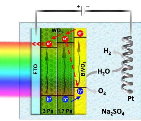
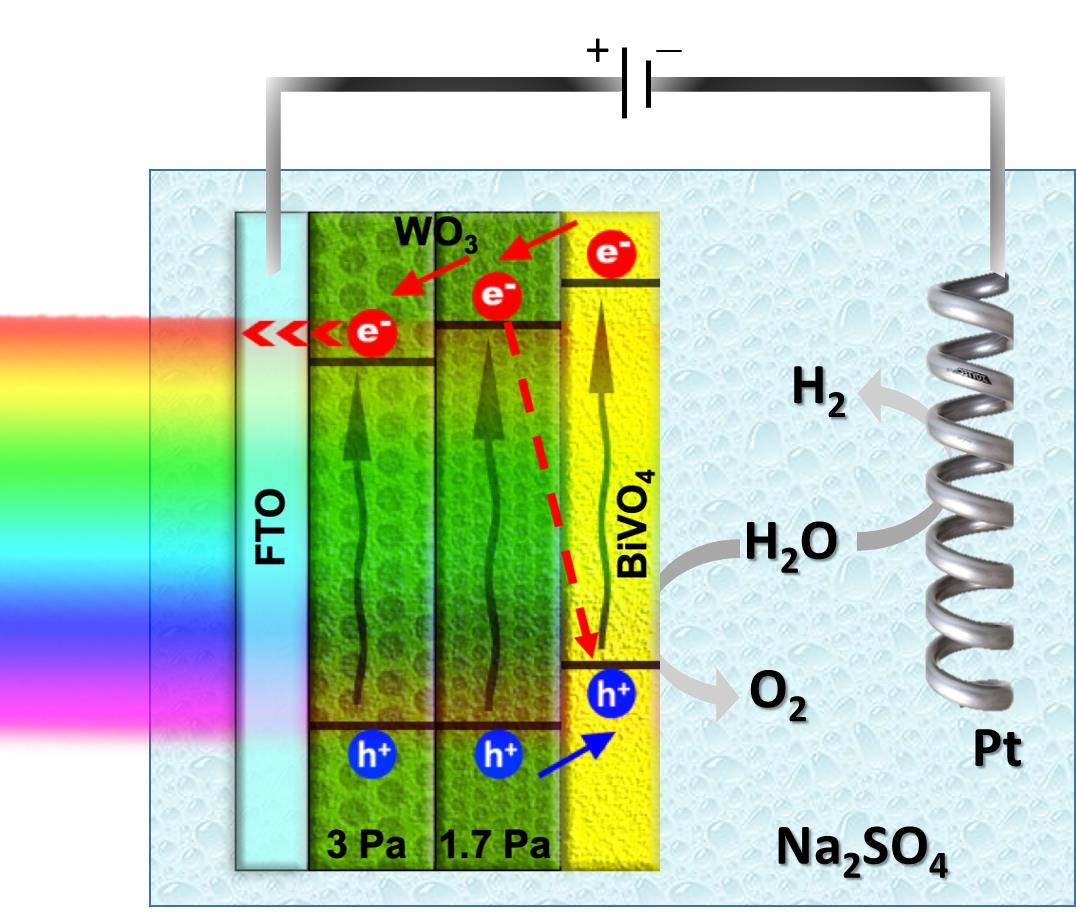
Multilayer WO3/BiVO4 Photoanodes for Solar-Driven Water Splitting Prepared by RF-Plasma Sputtering

1
CNR, Istituto per la Scienza e Tecnologia dei Plasmi, via R. Cozzi 53, 20125 Milano, Italy
2
Dipartimento di Chimica, Università degli Studi di Milano, via C. Golgi 19, 20133 Milano, Italy
*
Author to whom correspondence should be addressed.
Surfaces 2020, 3(1), 105-115; https://doi.org/10.3390/surfaces3010010
Submission received: 24 February 2020 / Revised: 10 March 2020 / Accepted: 11 March 2020 / Published: 13 March 2020
(This article belongs to the Special Issue Surface Aspects of Semiconductor Photochemistry)

Abstract

:
A series of WO3, BiVO4 and WO3/BiVO4 heterojunction coatings were deposited on fluorine-doped tin oxide (FTO), by means of reactive radio frequency (RF) plasma (co)sputtering, and tested as photoanodes for water splitting under simulated AM 1.5 G solar light in a three-electrode photoelectrochemical (PEC) cell in a 0.5 M NaSO4 electrolyte solution. The PEC performance and time stability of the heterojunction increases with an increase of the WO3 innermost layer up to 1000 nm. A two-step calcination treatment (600 °C after WO3 deposition followed by 400 °C after BiVO4 deposition) led to a most performing photoanode under back-side irradiation, generating a photocurrent density of 1.7 mA cm−2 at 1.4 V vs. SCE (i.e., two-fold and five-fold higher than that generated by individual WO3 and BiVO4 photoanodes, respectively). The incident photon to current efficiency (IPCE) measurements reveal the presence of two activity regions over the heterojunction with respect to WO3 alone: The PEC efficiency increases due to improved charge carrier separation above 450 nm (i.e., below the WO3 excitation energy), while it decreases below 450 nm (i.e., when both semiconductors are excited) due to electron–hole recombination at the interface of the two semiconductors.

Graphical Abstract

1. Introduction

With the rapid increase in the global energy demand and the tremendous climate concerns due to combustion of the limited fossil fuels reserves, there is an urgent need for clean and renewable energy sources [1,2]. The exploitation of hydrogen as an energy vector of the future is thought as an ideal solution for these problems [3,4]. However, to date, most of its production is based on steam reforming of natural gas which still involves massive amounts of CO2 emission, resulting environmentally unsustainable [5]. In this context, photoelectrochemical (PEC) water splitting is considered one of the most promising and green routes to harvest and convert solar energy through the production of H2 [6].
Among plenty of semiconductor materials suitable for the PEC water splitting reaction, BiVO4 has received significant attention in the last years due to its remarkable theoretical efficiency under visible light irradiation [7,8]. This is due to its narrow band gap of 2.4 eV, that extends its photoactivity up to 510 nm, and favorable band edges position. However, BiVO4 usually suffers low photocatalytic efficiency due to poor charge carriers mobility [9]. A possible solution to overcome this limitation is to couple BiVO4 with another semiconductor in order to form a heterojunction at the interface, achieving a spatial charge separation. Several semiconductors can be combined with BiVO4, including WO3 [10], SnO2 [11], Fe2O3 [12] and CdS [13]. Among these, WO3/BiVO4 is one of the most promising heterostructure, because both the valence and conduction bands of BiVO4 are located at a higher energy than those of WO3. Hence, a type II heterojunction is generated at the interface between the two semiconductor materials that allows efficient photo-promoted electron–hole separation [14]. Moreover, WO3 possesses a good electron transport ability of 12 cm2 V−1 s−1 with a moderate length of hole diffusion of ca. 150 nm [15]. Thus, in WO3/BiVO4 heterojunction, BiVO4 primarily acts as an excellent visible-light harvester up to 510 nm (i.e., ca. 30% of sunlight), while WO3 acts as efficient electron conductor. Several morphologies and preparation methods influencing the PEC activity of the WO3/BiVO4 heterojunction have been widely investigated and reported in literature so far. These include dense [10,14,16] and porous films [17,18], nanorods [19,20], helix [21] and inverse opal [22] structures. In particular, the highest photocurrent density reported so far (ca. 6.72 mA cm−2 at 1.23 V vs. RHE under 1 sun illumination) has been achieved over core-shell WO3/BiVO4 nanorods arrays decorated with a Co-Pi water oxidation co-catalyst system [23]. The WO3 nanorods arrays were prepared by RF magnetron sputtering under glancing angle deposition.
In the present work, a BiVO4 thin film was deposited by radio-frequency (RF) plasma co-sputtering [24] over a bilayer WO3 n-n heterojunction already optimized in our previous work [25]. The latter was obtained by plasma reactive sputtering, by depositing two consecutive layers of WO3 at different pressures. In fact, it was demonstrated that the deposition pressure affects the position of the conduction band (CB) energy of the material, resulting in a built-in electric field at the interface between the two WO3 layers. This obviously enhances the photo-promoted electron transfer.
The obtained WO3/BiVO4 system can, in principle, exploit the visible-light photoactivity of BiVO4 together with the efficient charge transport properties of the previously optimized WO3.
The effect that the WO3 bilayer thickness and the post calcination temperature have on the performance of WO3/BiVO4 photoanodes for water splitting was investigated under simulated AM 1.5 G solar light irradiation. The individual materials were also tested for comparison.

2. Materials and Methods

2.1. Photoanodes Preparation

The WO3 and BiVO4 individual photoanodes were prepared by RF diode plasma sputtering [26] and RF magnetron plasma co-sputtering [24], respectively. Both semiconductors were deposited on 10 × 10 mm2, 2 mm thick fluorine-doped tin oxide (FTO) conductive glass. For WO3 photoanodes preparation, the substrates were placed at 4.5 cm from the W (99.9%) metal target in a reactive environment (40% O2/Ar). The reactor was evacuated to less than 10−4 Pa before deposition. The sputtering power was set to 140 W and 1500 V of DC self-bias voltage. WO3 was grown with a bilayer deposition strategy using two different gas pressures. The first layer was deposited at 3 Pa, followed by the deposition of the second layer at 1.7 Pa. The deposition time was set in order to obtain three samples with a thickness of 200, 500 and 1000 nm. Each photoanode was formed by two layers with the same thickness. The photoelectrodes were then calcined in air at 600 °C for 2 h.
The BiVO4 films were deposited with a co-sputtering approach using separate bismuth oxide (Bi2O3, 99.9%) and metal vanadium (V, 99.99%) targets, 3.0 in. in diameter (Testbourne Ltd., Basingstoke, UK), with two separate power supplies in order to tune their power independently. The RF power of the metal vanadium target was fixed at 300 W (ca. 6 W/cm2), while that of Bi2O3 was fixed at 20 W (ca. 0.44 W/cm2). The FTO substrate was placed at 10 cm distance from the targets on a rotating substrate holder (1.5 rev/min) to guarantee a uniform deposition. The chamber was evacuated to less than 10−4 Pa before deposition. The deposition was performed in a 10% O2/Ar reactive mixture at a constant pressure of 1.7 Pa and for a deposition time necessary to achieve a thickness of 200 nm. The obtained photoelectrodes were then annealed in air at 400 or 600 °C for 2 h.
A series of heterojunction photoelectrodes was prepared by depositing a 200 nm-thick BiVO4 layer above the WO3 bilayer pre-calcinated at 600 °C for 2 h, with different thicknesses. After BiVO4 deposition, the photoelectrodes were calcinated at 400 °C for 2 h. Finally, one more heterojunction photoelectrode was prepared by depositing a 200 nm-thick BiVO4 layer above a pristine (i.e., not pre-annealed at 600 °C) 1000 nm-thick WO3 double layer and subsequently calcined at 600 °C for 2 h.

2.2. Photoanodes Characterization

In order to measure the film thickness, a portion of sample was covered with a silicon mask during deposition. After taking it away, the height difference between the deposited and non-deposited parts was measured with a P15 surface profilometer (KLA Tencor, San Jose, CA, USA).
The morphology of the photoelectrodes was investigated by scanning electron microscopy (SEM) using a LEO 1430 microscope (Zeiss, Jena, Germany) equipped with an INCA Energy Dispersive X-Ray Spectroscopy (EDX) Detector (Oxford Instruments, Buckinghamshire, UK) and by atomic force microscopy (AFM) in air by means of a Nano-RTM System Pacific Nanotechnology (Santa Clara, CA, USA). The AFM images were acquired in contact mode and the measurements were recorded at a scan speed of 0.5 µm/s for a scanned area of 5 × 5 µm2.
X-ray diffraction (XRD) patterns of the deposited coatings were recorded with a PW3020 powder diffractometer (Philips, Amsterdam, The Netherlands), using the Cu K radiation (λ = 1.5418 Å) .
UV-Vis diffuse reflectance spectra (DRS) were recorded in the 220–800 nm range with a UV3600 Plus spectrophotometer (Shimadzu, Kyoto, Japan) equipped with an ISR-603 integrating sphere, using barium sulfate as blank.

2.3. Photoelectrocatalytic Water Splitting Tests

The PEC activity was tested using a three-electrode homemade PEC cell, with the film deposited on FTO as working electrode, a Pt wire as counter electrode and a saturated calomel electrode (SCE) as reference. They were all connected to an Amel (Milan, Italy), mod. 2549 potentiostat/galvanostat and immersed in a 0.5 M Na2SO4 electrolyte solution. All measurements were performed under N2 bubbling into the electrolyte solution; N2 bubbling always started 20 min prior to the beginning of the tests. The samples were tested by means of linear sweep voltammetry (LSV, scan speed 5 mV s−1) and chronoamperometry (CA), both under simulated AM 1.5 G solar light (300 W LOT-qd Xe lamp, equipped with an AM 1.5 G filter). The photoanodes were placed at ca. 50 cm from the light source in order to have an incident power of 100 mWcm−2 on the photoactive surface. The incident photon to current efficiency (IPCE) curves were measured using the set-up described elsewhere [25]. The incident power was measured with a calibrated Thorlabs S130VC photodiode connected to a Thorlabs PM200 power meter. The electrodes were tested under both front- and back-side (i.e., through the FTO support) irradiation.

3. Results and Discussion

3.1. Photoanodes Characterization

The WO3 and BiVO4 coatings prepared as above described display the characteristic XRD peaks of the orthorhombic and monoclinic crystal structures, respectively, as already reported in our previous works [24,25]. The SEM micrograph of the cross section of the multilayer WO3/BiVO4/FTO photoanode (Figure 1a) confirms an overall film thickness of 1.28 μm due to a ca. 1.05 μm thick WO3 double layer and a ca. 238 nm-thick BiVO4 layer on top of it.
The EDX spectrum of the BiVO4 coatings reveals a V:Bi atomic ratio of 0.8, i.e., the coatings obtained under the adopted experimental conditions are Bi-rich. This result reflects the difficult tuning of the V:Bi atomic ratio during the co-sputtering process. The average surface roughness of the coating is 20 nm according to AFM measurements (Figure 1b). The UV-vis DRS spectra reported in Figure 1c show that the absorption edge of the individual WO3 coating is located at ca. 450 nm while that of BiVO4, calcined at either 400 or 600 °C, extends up to ca. 500 nm. The two heterojunction samples are dominated by the absorption properties of BiVO4. The direct band gap energy determined by the Tauc plot (Figure 1d) confirms that the two heterojunction samples show a band gap value similar to that of the single BiVO4 coating (i.e., ca. 2.5 eV; corresponding to a photon wavelength of 496 nm). The individual WO3 coating possesses a larger band gap energy of 2.8 eV, corresponding to a 443 nm wavelength.

3.2. PEC Performance of Individual WO3 and BiVO4 Photoanodes

The effect of the WO3 thickness on the LSV chopped curves is reported in Figure 2. The photocurrent density as a function of the applied potential on the as-prepared samples was recorded under both front (Figure 2a) and back (Figure 2b) irradiation. Similar PEC performances were obtained for the two modes of irradiation, proving an excellent photo-promoted electron transfer through the WO3 bilayer. The film thickness apparently does not significantly affect the PEC performance. However, during the subsequent chronoamperometry (CA) test at 1.0 V vs. SCE (Figure 2c), the photocurrent density significantly increases along the 3 h irradiation time, revealing a clear effect of the film thickness at the end of the run, the WO3 1000 nm-thick photoanode being the most performing one. This is reasonably due to the increasing light absorption capability with an increase of film thickness. The increasing PEC performance with increasing WO3 film thickness is further proved by the LSV curves recorded after CA tests (Figure 2d).
The BiVO4 photoanode shows a clear difference in photocurrent density between the two illumination conditions (Figure 3a,b), generating higher photocurrent when irradiated through FTO (back-side irradiation). This confirms the poor mobility of photo-promoted electrons through the BiVO4 material [27]. Moreover, the sample post-calcined at 600 °C shows a slightly higher performance than that calcined at 400 °C. The photoactivity of this BiVO4 coating is lower with respect to that of the best performing one reported in our previous work [24] prepared under similar sputtering conditions, due the Bi-rich atomic ratio of the here investigated material, revealed by EDX analysis. Indeed, the performance of BiVO4 is strongly affected by the Bi:V atomic ratio, stoichiometric 1:1 ratio materials being best performing. The time stability test (CA at 1.0 V vs. SCE, Figure 3c), though confirming the higher performance of the sample calcined at 600 °C, also reveals a partial loss of activity along the irradiation time. Interestingly, when the light is turned on the two samples generate a similar photocurrent density, but the BiVO4 coating post calcined at 600 °C shows a marked increase during the first 20 min of irradiation.
However, contrarily to WO3, when irradiation is chopped off (5 min in the dark), the gain of activity is progressively lost and stabilized after the fourth cycle of 30 min long irradiation. The LSV recorded under back irradiation after CA tests (Figure 3d) shows a decreased performance of the aged samples, as expected by the observed CA trend. Moreover, being the LSV a transient experiment, the performance of the two samples is similar, as expected by the similar photocurrent density generated during the CA experiment as the light is turned on.

3.3. PEC Performance of the WO3/BiVO4 Heterojunction

Figure 4 shows the PEC performance of the WO3/BiVO4 heterojunction as a function of the WO3 film thickness. All samples were annealed at 600 °C after WO3 deposition and at 400 °C after BiVO4 deposition. The PEC performance of the heterojunction electrodes shows a behavior partly common to those of individual WO3 and BiVO4 electrodes, namely: (i) Backside irradiation leads to higher generated photocurrent, as in the case of BiVO4 (Figure 4a,b); (ii) the PEC performance increases during CA tests, as in the case of WO3 (Figure 4c); and (iii) the performance increases with an increase of the WO3 double layer thickness. The highest photocurrent density (i.e., 1.05 mA cm−2 at 1.4 V vs. SCE) was attained with the 1000 nm-thick WO3 film illuminated from the backside.
The effect of the WO3 layer thickness becomes more evident after their stability test (Figure 4c,d). In fact, the WO3 1000 nm/BiVO4 sample benefits most from the “photo-assisted activation”, reaching a maximum photocurrent of 1.7 mA cm−2 at 1.4 V vs. SCE (Figure 4c), with an 80% increase with respect to the as-prepared heterojunction electrode. This corresponds to ca. two-fold and to ca. five-fold increase compared to the photocurrent produced by individual 1000 nm-thick WO3 (0.8 mA cm−2) and BiVO4 (0.35 mA cm−2), respectively. Moreover, the overall photocurrent density generated by the heterojunction electrode significantly exceeds the sum of the photocurrent densities generated by the individual semiconductors (Figure 5). Thus, it confirms the capability of the heterojunction structure to attain an efficient space separation of the charge carriers due to the optimal band alignment of these two semiconductor materials.
Finally, we explored the effect of the post calcination temperature on the PEC performance of the heterojunction photoanodes (Figure 5).
Two samples were prepared under the same WO3 and BiVO4 sputtering conditions. One sample was post annealed at 600 °C for 2 h after WO3 deposition over FTO and then at 400 °C for 2 h after BiVO4 deposition (as the above investigated series of samples). This sample is labelled as WO3/BiVO4_400C. The other sample was subjected to a single-step post calcination treatment at 600 °C for 2 h after BiVO4 deposition above WO3 (WO3/BiVO4_600C). Figure 5 shows that the post calcination procedure strongly affects the PEC performance of the heterojunction. Surprisingly, WO3/BiVO4_600C displays similar efficiency under both front and backside irradiation, reaching ca. 1 mA cm−2 photocurrent density at 1.4 V vs. SCE over the as-prepared sample. Moreover, the sample annealed at 600 °C generates ca. two-fold photocurrent density with respect to that annealed at 400 °C under front irradiation, while the two samples show similar activity under backside irradiation. The post calcination protocol affects the time stability of the samples as well. WO3/BiVO4_600C suffers from partial deactivation along the irradiation time similar to that of BiVO4_600C (Figure 5c). Hence, the sample calcined at 600 °C shows a similar activity to WO3 after CA tests, which is half of the photocurrent generated by WO3/BiVO4_400C (Figure 5d).
The IPCE curves recorded after CA tests (Figure 6) help to get a deeper insight into the different PEC performances of these two heterojunction samples.
The onset photoactivity of WO3 and of BiVO4 are below 450 and 500 nm, respectively, in agreement with their band gap energy determined by the Tauc plot. BiVO4_600C shows higher IPCE under backside irradiation with a maximum of 6% at 350 nm. On the other hand, the WO3 double layer confirms to be a good performing photoanode, with a maximum IPCE of 90% at 350 nm under backside irradiation. Both heterojunction samples post-calcined at different temperatures display a significantly improved photoactivity in the 450–500 nm range (i.e., in the photon energy range below the WO3 absorption onset). This result highlights the role of the WO3 double layer in improving the photoactivity of BiVO4 by providing a downhill pathway in the CB levels that allows an efficient electron–hole separation, as shown in Scheme 1a. Interestingly, the IPCE of the WO3/BiVO4_600C sample in this spectral region is higher than the IPCE of the WO3/BiVO4_400C sample, especially under front-side irradiation. However, at higher photon energy (i.e., below the WO3 absorption threshold), both heterojunction photoanodes exhibit an IPCE lower than the WO3 coating alone. This phenomenon has been already reported in the literature [14,28] and attributed [29,30] to an electron–hole recombination path occurring at the interface when both semiconductors are excited, as depicted in Scheme 1b. Interestingly, the two heterojunction samples display very different behaviors in the high photon energy region (λ < 450 nm) under front- or back-side irradiation. Indeed, the WO3/BiVO4_600C sample keeps a relatively high IPCE under front-side irradiation, reaching a maximum of 23% at 370 nm, with a minor loss with respect to single WO3. In contrast, under back-side irradiation the same photoelectrode shows a maximum IPCE of 27% at 440 nm (i.e., in correspondence of the WO3 absorption onset), followed by a dramatic loss of efficiency at lower wavelengths, while WO3/BiVO4_400C shows an increasing IPCE up to 60% at 350 nm (though lower than that of WO3 alone). This dramatic loss of efficiency of the WO3/BiVO4_600C sample below 450 nm is responsible for its relative low PEC performance under simulated solar light, as shown in Figure 5c,d. This result suggests that the single step post annealing treatment at 600 °C very likely produces a better contact at the interface between the two semiconductor materials that favors a more efficient electron transfer at λ > 450 nm (Scheme 1a), but also a higher probability of charge carriers recombination (according to Scheme 1b) when both semiconductors are excited (i.e., λ < 450 nm). The higher IPCE attained with this sample under front-side irradiation reflects its intrinsic higher efficiency, because under this irradiation mode, even at λ < 450 nm, the largest part of the photons are absorbed by the outermost BiVO4 layer, thus reducing the probability of electron–hole recombination at the interface.

4. Conclusions

Reactive RF plasma (co)sputtering demonstrates to be an effective technique for the deposition of multilayered WO3/BiVO4 heterojunction photoanodes for solar-driven water splitting. This can open the way to a future scale-up of the PEC technology by deposition of large surface area photoanodes. The thickness of the WO3 double layer, the post annealing treatment and the irradiation mode (back- or front-side) strongly affect the efficiency of the WO3/BiVO4 heterojunction. In this work, the best performing heterojunction was obtained by a two-step annealing treatment (i.e., over a 1000 nm-thick WO3 double layer calcined at 600 °C followed by deposition of a 200 nm-thick BiVO4 layer further calcined at 400 °C). The electron–hole recombination at the interface between the two semiconductors occurring at photon energy above the WO3 band gap was confirmed to be the main drawback of this system, especially for heterojunction photoanodes prepared in a single-step calcination treatment at 600 °C. Nonetheless, coupling two semiconductor materials with appropriate bands alignment confirms to be a very promising approach to improve charge carrier separation and, hence, significantly increase the PEC performance under solar light irradiation.

Author Contributions

M.P. prepared the samples supervised by E.V.; G.L.C. performed the PEC and IPCE measurements and wrote the manuscript together with M.P.; G.L.C. and E.S. conceived the experiments; E.S. supervised the project and optimized the final version of the manuscript. All authors have read and agreed to the published version of the manuscript.

Funding

This research was funded by “Ministero dell’istruzione, dell’università e della ricerca, MIUR”, PRIN2017, grant number 20179337R7 (MULTI-e project)” and PRIN2015, grant number 2015K7FZLH (Solar-driven chemistry: new materials for photo- and electro-catalysis). It was also supported by the University of Milano through the project PSR2017, linea 2, Azione A” and within the CNR-Regione Lombardia Agreement No. 19366/RCC, January 10th, 2017, Decr. Reg. No. 7784—05/08/2016.

Acknowledgments

The authors thank the UNITECH NoLimits and Nadia Santo for the SEM investigation. The very active and skillful collaboration of Alessandro Zizzi and Filippo Maggi in the experimental part of the work is acknowledged.

Conflicts of Interest

The authors declare no conflicts of interest.

References

  1. Marszewski, M.; Cao, S.; Yu, J.; Jaroniec, M. Semiconductor-based photocatalytic CO2 conversion. Mater. Horizons 2015, 2, 261–278. [Google Scholar] [CrossRef]
  2. Li, X.; Wen, J.; Low, J.; Fang, Y.; Yu, J. Design and fabrication of semiconductor photocatalyst for photocatalytic reduction of CO2 to solar fuel. Sci. China Mater. 2014, 57, 70–100. [Google Scholar] [CrossRef] [Green Version]
  3. Furukawa, H.; Yaghi, O.M. Storage of hydrogen, methane, and carbon dioxide in highly porous covalent organic frameworks for clean energy applications. J. Am. Chem. Soc. 2009, 131, 8875–8883. [Google Scholar] [CrossRef] [PubMed]
  4. Chalk, S.G.; Miller, J.F. Key challenges and recent progress in batteries, fuel cells, and hydrogen storage for clean energy systems. J. Power Sources 2006, 159, 73–80. [Google Scholar] [CrossRef]
  5. Ganguly, P.; Harb, M.; Cao, Z.; Cavallo, L.; Breen, A.; Dervin, S.; Dionysiou, D.D.; Pillai, S.C. 2D Nanomaterials for Photocatalytic Hydrogen Production. ACS Energy Lett. 2019, 4, 1687–1709. [Google Scholar] [CrossRef] [Green Version]
  6. Hisatomi, T.; Kubota, J.; Domen, K. Recent advances in semiconductors for photocatalytic and photoelectrochemical water splitting. Chem. Soc. Rev. 2014, 43, 7520–7535. [Google Scholar] [CrossRef]
  7. Sivula, K.; van de Krol, R. Semiconducting materials for photoelectrochemical energy conversion. Nat. Rev. Mater. 2016, 1, 15010. [Google Scholar] [CrossRef]
  8. Huang, Q.; Ye, Z.; Xiao, X. Recent progress in photocathodes for hydrogen evolution. J. Mater. Chem. A 2015, 3, 15824–15837. [Google Scholar] [CrossRef]
  9. Chen, L.; Alarcón-Lladó, E.; Hettick, M.; Sharp, I.D.; Lin, Y.; Javey, A.; Ager, J.W. Reactive sputtering of bismuth vanadate photoanodes for solar water splitting. J. Phys. Chem. C 2013, 117, 21635–21642. [Google Scholar] [CrossRef] [Green Version]
  10. Grigioni, I.; Stamplecoskie, K.G.; Selli, E.; Kamat, P.V. Dynamics of photogenerated charge carriers in WO3/BiVO4 heterojunction photoanodes. J. Phys. Chem. C 2015, 119, 20792–20800. [Google Scholar] [CrossRef]
  11. Chatchai, P.; Murakami, Y.; Kishioka, S.-Y.; Nosaka, A.Y.; Nosaka, Y. FTO∕SnO2∕BiVO4 composite photoelectrode for water oxidation under visible light irradiation. Electrochem. Solid State Lett. 2008, 11, H160. [Google Scholar] [CrossRef]
  12. Xia, L.; Bai, J.; Li, J.; Zeng, Q.; Li, L.; Zhou, B. High-performance BiVO4 photoanodes cocatalyzed with an ultrathin α-Fe2O3 layer for photoelectrochemical application. Appl. Catal. B Environ. 2017, 204, 127–133. [Google Scholar] [CrossRef]
  13. Li, L.-P.; Liu, M.; Zhang, W.-D. Electrodeposition of CdS onto BiVO4 films with high photoelectrochemical performance. J. Solid State Electrochem. 2018, 22, 2569–2577. [Google Scholar] [CrossRef]
  14. Seo, J.H.; Park, G.; Oh, K.H.; Kang, S.H.; Lee, H.C.; Cho, S.K.; Nam, K.M. Analysis of charge separation processes in WO3 -BiVO4 composite for efficient photoelectrochemical water oxidation. J. Electroanal. Chem. 2017, 789, 17–23. [Google Scholar] [CrossRef]
  15. Huang, Z.; Song, J.; Pan, L.; Zhang, X.; Wang, L.; Zou, J. Tungsten oxides for photocatalysis, electrochemistry, and phototherapy. Adv. Mater. 2015, 27, 5309–5327. [Google Scholar] [CrossRef] [PubMed]
  16. Hong, S.J.; Lee, S.; Jang, J.S.; Lee, J.S. Heterojunction BiVO4/WO3 electrodes for enhanced photoactivity of water oxidation. Energy Environ. Sci. 2011, 4, 1781. [Google Scholar] [CrossRef] [Green Version]
  17. Fujimoto, I.; Wang, N.; Saito, R.; Miseki, Y.; Gunji, T.; Sayama, K. WO3/BiVO4 composite photoelectrode prepared by improved auto-combustion method for highly efficient water splitting. Int. J. Hydrogen Energy 2014, 39, 2454–2461. [Google Scholar] [CrossRef]
  18. Chae, S.Y.; Lee, C.S.; Jung, H.; Joo, O.-S.; Min, B.K.; Kim, J.H.; Hwang, Y.J. Insight into charge separation in WO3/BiVO4 heterojunction for solar water splitting. ACS Appl. Mater. Interfaces 2017, 9, 19780–19790. [Google Scholar] [CrossRef]
  19. Pilli, S.K.; Janarthanan, R.; Deutsch, T.G.; Furtak, T.E.; Brown, L.D.; Turner, J.A.; Herring, A.M. Efficient photoelectrochemical water oxidation over cobalt-phosphate (Co-Pi) catalyst modified BiVO4/1D-WO3 heterojunction electrodes. Phys. Chem. Chem. Phys. 2013, 15, 14723. [Google Scholar] [CrossRef]
  20. Pihosh, Y.; Turkevych, I.; Mawatari, K.; Asai, T.; Hisatomi, T.; Uemura, J.; Tosa, M.; Shimamura, K.; Kubota, J.; Domen, K.; et al. Nanostructured WO3/BiVO4 photoanodes for efficient photoelectrochemical water splitting. Small 2014, 10, 3692–3699. [Google Scholar] [CrossRef]
  21. Shi, X.; Choi, I.Y.; Zhang, K.; Kwon, J.; Kim, D.Y.; Lee, J.K.; Oh, S.H.; Kim, J.K.; Park, J.H. Efficient photoelectrochemical hydrogen production from bismuth vanadate-decorated tungsten trioxide helix nanostructures. Nat. Commun. 2014, 5, 4775. [Google Scholar] [CrossRef] [Green Version]
  22. Zhang, H.; Zhou, W.; Yang, Y.; Cheng, C. 3D WO3/BiVO4/Cobalt phosphate composites inverse opal photoanode for efficient photoelectrochemical water splitting. Small 2017, 13, 1603840. [Google Scholar] [CrossRef]
  23. Pihosh, Y.; Turkevych, I.; Mawatari, K.; Uemura, J.; Kazoe, Y.; Kosar, S.; Makita, K.; Sugaya, T.; Matsui, T.; Fujita, D.; et al. Photocatalytic generation of hydrogen by core-shell WO3/BiVO4 nanorods with ultimate water splitting efficiency. Sci. Rep. 2015, 5, 11141. [Google Scholar] [CrossRef] [Green Version]
  24. Pedroni, M.; Chiarello, G.L.; Haghshenas, N.; Canetti, M.; Ripamonti, D.; Selli, E.; Vassallo, E. Bismuth vanadate photoanodes for water splitting deposited by radio frequency plasma reactive co-sputtering. J. Vac. Sci. Technol. B 2020, 38, 012203. [Google Scholar] [CrossRef]
  25. Chiarello, G.L.; Bernareggi, M.; Pedroni, M.; Magni, M.; Pietralunga, S.M.; Tagliaferri, A.; Vassallo, E.; Selli, E. Enhanced photopromoted electron transfer over a bilayer WO3 n–n heterojunction prepared by RF diode sputtering. J. Mater. Chem. A 2017, 5, 12977–12989. [Google Scholar] [CrossRef]
  26. Pedroni, M.; Canetti, M.; Chiarello, G.L.; Cremona, A.; Inzoli, F.; Luzzati, S.; Pietralunga, S.M.; Tagliaferri, A.; Zani, M.; Vassallo, E. Tungsten oxide thin film photo-anodes by reactive RF diode sputtering. Thin Solid Films 2016, 616, 375–380. [Google Scholar] [CrossRef]
  27. Luo, W.; Yang, Z.; Li, Z.; Zhang, J.; Liu, J.; Zhao, Z.; Wang, Z.; Yan, S.; Yu, T.; Zou, Z. Solar hydrogen generation from seawater with a modified BiVO4 photoanode. Energy Environ. Sci. 2011, 4, 4046. [Google Scholar] [CrossRef]
  28. Grigioni, I.; Dozzi, M.V.; Selli, E. Photoinduced electron transfer in WO3/BiVO4 heterojunction photoanodes: effects of the WO3 layer thickness. J. Phys. Condens. Matter 2020, 32, 014001. [Google Scholar] [CrossRef]
  29. Grigioni, I.; Stamplecoskie, K.G.; Jara, D.H.; Dozzi, M.V.; Oriana, A.; Cerullo, G.; Kamat, P.V.; Selli, E. Wavelength-Dependent Ultrafast Charge Carrier Separation in the WO3/BiVO4 Coupled System. ACS Energy Lett. 2017, 2, 1362–1367. [Google Scholar] [CrossRef] [Green Version]
  30. Grigioni, I.; Abdellah, M.; Corti, A.; Dozzi, M.V.; Hammarström, L.; Selli, E. Photoinduced Charge-Transfer Dynamics in WO3/BiVO4 Photoanodes Probed through Midinfrared Transient Absorption Spectroscopy. J. Am. Chem. Soc. 2018, 140, 14042–14045. [Google Scholar] [CrossRef] [Green Version]
Figure 1. (a) Cross section SEM and (b) top view AFM images of WO3/BiVO4_400 °C; (c) UV-vis reflectance spectra and (d) Tauc plots for direct band gap of the investigated samples.
Surfaces 03 00010 g001
Figure 2. Effect of the WO3 film thickness on chopped Linear Sweep Voltammetry (LSV) curves under (a) front and (b) back irradiation of as-prepared samples; (c) chronoamperometry (CA) stability test at 1.0 V vs. SCE; (d) chopped LSV curves under back irradiation recorded after CA tests (panel c). All measurements were made in a 0.5 M Na2SO4 electrolyte solution under simulated AM 1.5 G solar irradiation.
Surfaces 03 00010 g002
Figure 3. Effect of the post calcination temperature (400 or 600 °C) of the BiVO4 film on chopped Linear Sweep Voltammetry (LSV) curves under (a) front and (b) back irradiation of as-prepared samples; (c) chronoamperometry (CA) tests at 1.0 V vs. SCE; (d) chopped LSV curves under back irradiation recorded after CA tests (panel c). All measurements were made in a 0.5 M Na2SO4 electrolyte solution under simulated AM 1.5 G solar irradiation.
Surfaces 03 00010 g003
Figure 4. Effect of the WO3 film thickness on the photoelectrochemical (PEC) performance of the WO3/BiVO4 heterojunctions: Chopped Linear Sweep Voltammetry (LSV) curves under (a) front and (b) back irradiation of as-prepared samples; (c) chronoamperometry (CA) tests at 1.0 V vs. SCE; (d) chopped LSV curves under back irradiation recorded after CA tests (panel c). All samples were post calcined at 400 °C for 2 h after BiVO4 deposition. All measurements were made in a 0.5 M Na2SO4 electrolyte solution under simulated AM 1.5 G solar irradiation.
Surfaces 03 00010 g004
Figure 5. Effect of the post calcination temperature (400 or 600 °C) on the photoelectrochemical (PEC) performance of the WO3/BiVO4 heterojunctions: Chopped Linear Sweep Voltammetry (LSV) curves under (a) front and (b) back irradiation of as-prepared samples; (c) chronoamperometry (CA) stability tests at 1.0 V vs. SCE; (d) chopped LSV curves under back irradiation recorded after CA tests (panel c). The WO3 and BiVO4 film thicknesses were 1000 and 200 nm, respectively. All measurements were made in a 0.5 M Na2SO4 electrolyte solution under simulated AM 1.5 G solar irradiation.
Surfaces 03 00010 g005
Figure 6. Incident photon to current efficiency (IPCE) curves recorded with WO3 (red line), WO3/BiVO4_400C (green line), WO3/BiVO4_600C (blue line) and BiVO4_600C (black line) photoanodes under (a) front- and (b) back-side irradiation at 1.0 V vs. SCE in a 0.5 M Na2SO4 electrolyte solution.
Surfaces 03 00010 g006
Scheme 1. Effect of the irradiation wavelength on the pathways of photogenerated electron–hole pairs in multilayer WO3/BiVO4 photoanodes: Spatial electron–hole separation at the WO3/BiVO4 heterojunction under irradiation at wavelengths (a) above and (b) below 450 nm. Under excitation of both semiconductors, a possible recombination channel opens at the interface, between electrons photo-promoted in the WO3 conduction band (CB) and holes photoproduced in the BiVO4 valence band (VB), hindering the overall PEC performance.
Surfaces 03 00010 sch001

