Article

Spatially Resolved XPS Characterization of Electrochemical Surfaces

1
Dipartimento di Ingegneria dell’Innovazione, Università del Salento, v. Monteroni, 73100 Lecce, Italy
2
Jožef Stefan Institute, Jamova cesta 39, 1000 Ljubljana, Slovenia
3
Elettra - Sinctrotrone Trieste S.C.p.A. S.S. 14, km 163.5 in Area Science Park, 34149 Trieste-Basovizza, Italy
4
Institute of Physical Chemistry, Bulgarian Academy of Sciences, 1113 Sofia, Bulgaria
*
Author to whom correspondence should be addressed.
Surfaces 2019, 2(2), 295-314; https://doi.org/10.3390/surfaces2020022
Submission received: 20 February 2019 / Revised: 5 April 2019 / Accepted: 9 April 2019 / Published: 15 April 2019
(This article belongs to the Special Issue Electrochemical Surface Science: Basics and Applications)

Abstract

:
Synchrotron-based scanning photoelectron microscopy (SPEM) has opened unique opportunities for exploiting processes occurring at surfaces and interfaces, which control the properties of materials for electrochemical devices, where issues of chemical and morphological complexity at microscopic length scales should be faced and understood. The present article aims to demonstrate the present capabilities of SPEM to explore the surface composition of micro- and nano-structured materials, focusing on cases relevant to electrochemical technologies. We report and discuss a selection of recent results about three different systems, targeting hot topics in the fields of electrochemical energy storage and electrochemical fabrication: (i) an in-depth analysis of Ag-In electrodeposited alloys exhibiting dynamic pattern formation, (ii) the analysis of electrochemical processes at the electrodes of a self-driven solid oxide fuel cell and (iii) an operando characterization of a single-chamber solid oxide fuel cell. The last example has been performed at near-ambient pressure conditions using a unique specially designed setup which extends the traditional capabilities of scanning photoemission microscopes in the ultra-high and high-vacuum regimes to operating conditions that are closer to realistic ones, contributing to overcome the so-called “pressure gap”.

Graphical Abstract

1. Introduction

The ubiquitous and enabling role of electrochemical technologies in many different fields of technology [1], but especially in energy storage [2], cannot be overemphasized. Electrochemical processes and the devices in which they are implemented are highly complex systems in which successful functioning is the result of the cooperation of different types of physics interacting on a range of diverse space- and time-scales. The complex nature of electrochemical systems generally makes the task of understanding and optimizing them an extremely challenging one. One of the main difficulties underlying electrochemistry is the necessity of transferring charge between electrically and ionically conducting phases in processes that are coupled with chemical reactions and phase-transformations. Moreover, these complex processes occur mainly at the electrode–electrolyte interface and involve thin layers of material. In these regions structural, chemical and electronic properties of the materials may significantly deviate from the intrinsic bulk ones. An additional obstacle in the characterization of the reactive interfaces is their position: they are often buried and not easily accessible without disturbing the functionally relevant chemical and structural ambient. In the last decades, traditional bulk-sensitive analysis tools, in particular, X-ray diffraction or fluorescence spectromicroscopy, largely employed in the characterization of electrochemical systems, have been more extensively supported by X-ray based surface sensitive techniques such as X-ray photoelectron spectroscopy (XPS) which can maximize the information confined in thin layers [3]. XPS was initially conceived as a spectroscopy technique necessarily requiring operation in ultra-high vacuum (UHV) or at least high-vacuum (HV) ambient and it was developed and implemented with this approach for many decades. But, as for other fields of science and technology, a state-of-the-art method for the investigation of electrochemical systems should tackle the so-called “material gap” and “pressure gap”. The first one is linked to the development of nanomaterials and nanotechnology and the corresponding need of understanding processes at the nanoscale, while the latter aims to analyze an electrochemical reaction in the real pressure working regime. The latter is a challenge for many vacuum-based characterization techniques. In recent years a lot of efforts have been put in trying to overcome the two limitations for XPS, with the successful outcome of developing novel approaches.
The fast progress in the development and implementation of photoelectron spectromicroscopy techniques, i.e., adding spatial resolution and imaging capabilities to XPS, started in the last decade of the 20th century with the construction of low emittance X-ray synchrotron machines, providing tunable energy photon beams with very high brightness and variable polarization [4,5]. Thanks to the high photon intensity provided by insertion devices it has become possible to add sub-micrometer lateral resolution to XPS, realizing new instruments called photoelectron microscopes [6]. In X-ray photoelectron microscopes high spatial resolution is achieved using either full-field or scanning methods. In scanning instruments, called scanning photoelectron microscopes (SPEM), the photon beam is demagnified to sub-micrometer dimensions using suitable photon optics. Modern SPEMs can achieve spatial resolutions as low as 70–100 nm, allowing full material characterization at the nanoscale [7,8]; despite the fact that full-field photoemission microscopes can achieve even better lateral resolutions (20–30 nm), they impose severe constraints in the sample geometry and morphology which, instead, do not affect the performance of scanning ones. This flexibility with respect to sample requirements is particularly crucial for the operando characterization of electrochemical systems. Since its construction in the mid of 90’s, the soft X-ray SPEM at the Elettra synchrotron research center has investigated many electrochemical systems based on solid state electrolytes and electrodes in the standard UHV or HV environment, often in operando conditions [9,10,11] demonstrating how the material gap can be successfully overcome in the characterization of electrochemical systems. With respect to the pressure gap problem in XPS, a fundamental contribution to overcome it was achieved with the development of the differentially-pumped electron analyzers at the beginning of this century; after almost 20 years of advances, XPS analysis at pressures as high as several tens of millibar can be performed in gas and liquid environments not only at synchrotron beamlines but also with conventional instruments [12,13].
In addition to standard near-ambient pressure XPS approaches (generally denoted by the acronym APXPS) to the characterization of electrochemical systems, now largely diffused [14,15,16], it is worthwhile to mention a couple of developments particularly adaptable to electrochemistry: (i) the implementation of hard X-rays XPS, which allows spectroscopy investigation of deeper layers [17] such as buried interfaces and (ii) the “dip and tip” method to study solid-liquid interfaces [18,19], available at few synchrotron beamlines. In spite of their innovation all these approaches fail in combining APXPS with submicron spatial resolution; this technological problem started to be solved as recently as in the last decade thanks to the efforts of the team of the Escamicroscopy beamline at Elettra which allowed the development and implementation of innovative technical solutions for SPEM, capable of performing near-ambient pressure photoemission spectromicroscopy while keeping the typical SPEM performance [20,21].
This manuscript is presenting three examples of electrochemical experiments performed with SPEM in three different environmental conditions. In the first experiment, the characterization of an ex situ electrodeposited Ag-In alloy, exhibiting a dynamic pattern formation mechanism, has been performed. In the second experiment the electrochemical processes at the electrodes of a self-driven solid oxide fuel cell (SOFC) have been analyzed; in this case the operando condition was achieved in HV pressure regimes, while the last case reports on the operando characterization of a single-chamber solid oxide fuel cell (SC-SOFC) at near-ambient pressure conditions, using a newly developed cell.

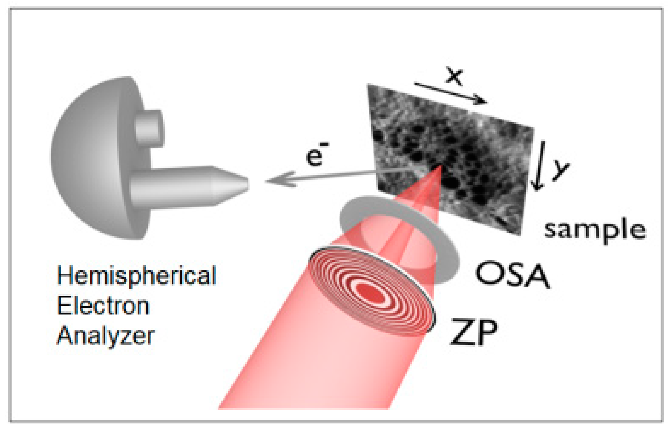
2. Materials and Methods: the Soft X-rays Scanning Photoemission Microscope of Elettra

2.1. The Standard UHV—HV Setup

The standard configuration of the SPEM was originally designed to work in UHV conditions; a schematic view of the focusing optics and photoelectron detection systems of the SPEM of the Escamicroscopy beamline at Elettra is shown in Figure 1. The X-ray beam is focused on the sample using a diffractive lens called zone plate (ZP), which allows to achieve a spot diameter of ~130 nm as best performance. In the typical experiment the X-ray spot impinges normally to the sample even if a polar rotation is possible. While samples are raster-scanned with respect to the X-ray microprobe, the photoelectrons generated at the sample surface are collected and energy-selected by means of a hemispherical electron analyzer (HEA), equipped with a 48-channels electron detector [22]. The takeoff angle of photoelectrons is fixed to 30°. This configuration strongly enhances the surface sensitivity of the SPEM because due to inelastic collisions only photoelectrons generated in the topmost layers can reach the HEA. A SPEM can be operated in two modes: (i) imaging spectromicroscopy and (ii) microspot spectroscopy. The imaging mode maps the lateral distribution of elements by collecting photoelectrons within a selected kinetic energy window while scanning the specimen with respect to the microprobe. By properly setting the energy range, the distribution of the chemical states of a selected element can be measured, in addition to that of the bare elemental concentration. The microspot mode is similar to conventional XPS, i.e., energy distribution curves are measured from the illuminated local micro-spot area selected within an image.
In this configuration, the samples are exposed to the common environment of the analysis chamber, which hosts the focusing optics, the HEA and other ancillary equipment; the highest allowable pressure in the case of experiments where samples need to be exposed to gases is about 1 × 10⁻⁵ mbar.

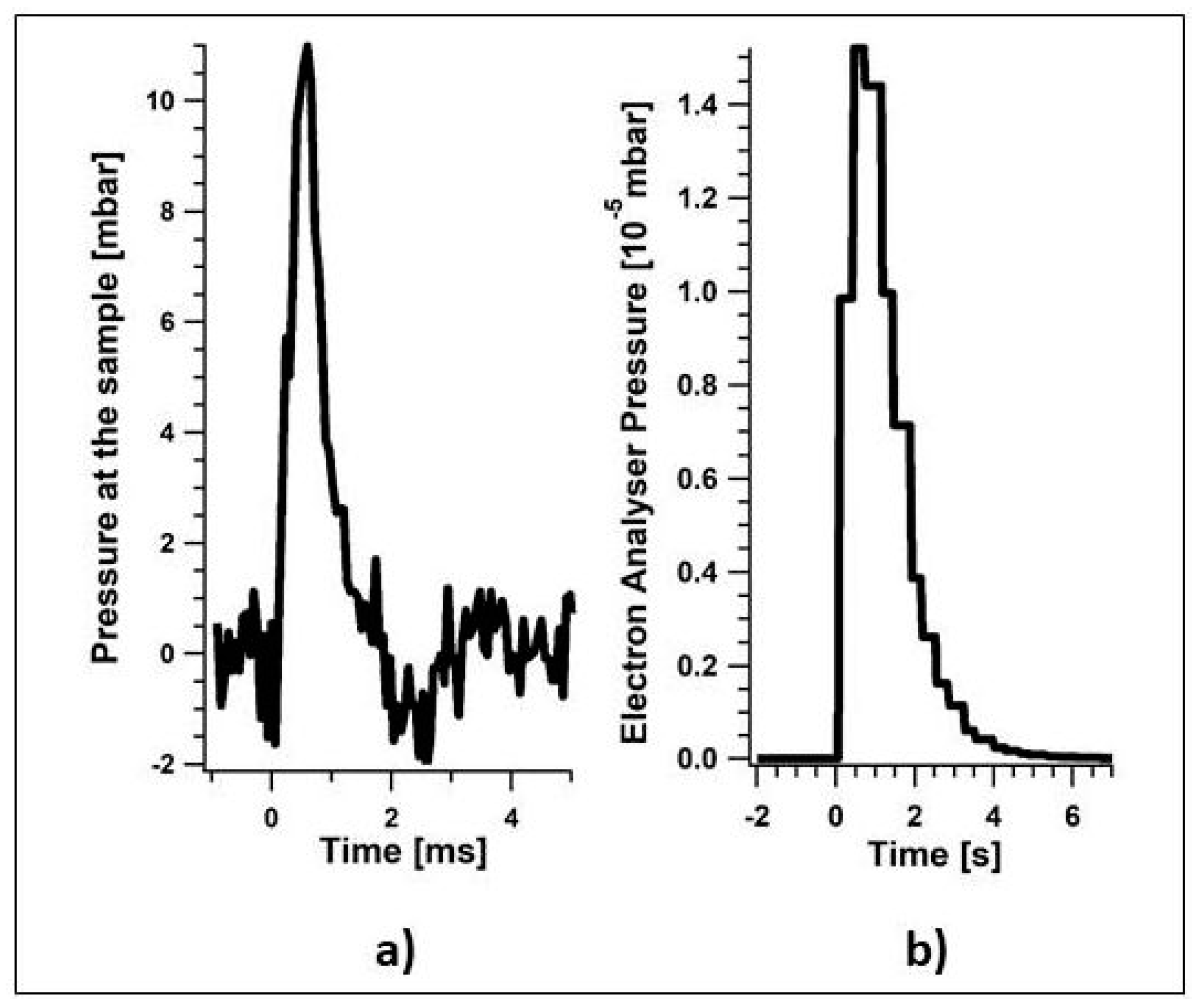
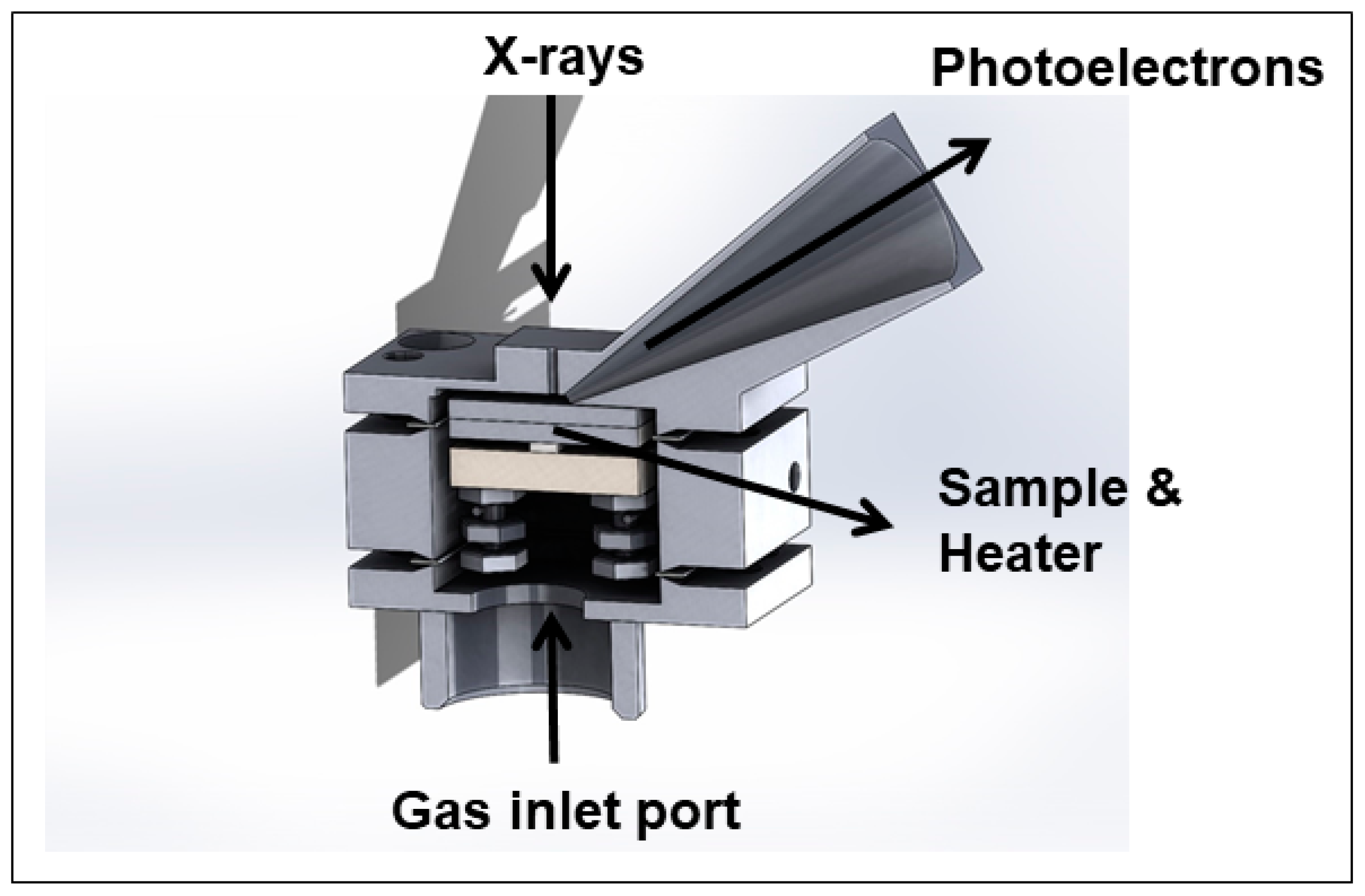
2.2. Novel Solutions for Operando Near-ambient Pressure Approaches

The typical photon energies and ZP dimensions used in the SPEM imply distances between ZP and samples of a few mm. Moreover, an additional pinhole, the order-sorting aperture (OSA), located between the ZP and the sample, is necessary to select a single diffracted spot. These geometrical constraints are the main reason why the technical solutions found to overcome the “pressure gap” for XPS setups could not be transferred straightforwardly to SPEMs. At Elettra two special setups have been recently developed, allowing experiments in near-ambient pressure conditions, preserving the best achievable spatial resolution: (i) the Dynamic High Pressure (DHP) setup and (ii) the Near-Ambient Pressure Cell (NAP-Cell).
The DHP system uses a highly collimated gas jet as a supersonic jet expansion into the SPEM vacuum chamber [23]; gases are confined into a narrow beam and point to the sample surface by using a pulsed jet instead of a continuous one. Similar setups have been already used in other research fields to control the amount of injected gases [24,25]. The DHP set-up has been designed to fit into the SPEM chamber: the gas jet is generated in the region around the sample by a thin needle connected to a pulsed valve which produces a series of gas jet shots at a fixed repetition rate. Each shot gives rise to a short burst of pressure in a small and confined volume near the sample and to an increase of the background pressure in the SPEM chamber. By finely tuning (i) the shot duration, (ii) the sample-to-needle distance and (iii) the DHP gas line pressure, the pressure at the sample can be controlled, while the injected gas is efficiently diluted into the large chamber volume, so that the background pressure does not exceed the HV limit in the analyzer. Figure 2 shows a typical single-shot pressure time-profile at the sample surface for a pulsed valve aperture time of 3.2 ms and the corresponding SPEM background pressure. The distance between the sample and the needle tip was fixed to 2 mm and the pressure of the gas in the DHP gas line was 3.5 bar. As shown in Panel (a), in these conditions the sample surface is experiencing a gas environment of ~10 mbar for a few ms. The corresponding change in the SPEM pressure is reported in Panel (b). A valve aperture frequency of 0.35 Hz is needed to keep the SPEM background pressure within the limit of ~1 × 10⁻⁵ mbar. More details can be found in ref [21].
To address experiments where a constant pressure value is needed, the NAP-Cell has been developed. This device consists of a small vacuum-sealed cell - in which the sample is encapsulated-equipped with small pinholes as photon-in/photoelectron-out apertures [20]. A sectional view of this setup is shown in Figure 3. The gases needed in the experiment are delivered into the cell through a flexible metal bellow which terminates the dosing line located inside the SPEM chamber. A gas-dosing system allows regulation of the gas flow into the line at the desired flux/pressure. An encapsulated heater allows to heat up the sample, at the back of which it is placed, to temperatures up to 900–950 K. Additional electrical contacts are available for biasing samples in electrochemical setups. A pressure gap between the SPEM vacuum chamber and the inner volume of the NAP-Cell is established by the impedance induced by the small pinholes, which makes it possible to reach NAP conditions (~0.1 mbar) inside the cell while maintaining HV condition outside it (10−5 mbar). It is worth noting that, at variance with a standard NAP setup for spectroscopy, a differentially-pumped electron analyzer is not needed.
Regarding the microscopy capability, the entire cell is scanned with respect to the X-rays beam, as for conventional UHV experiments. The “visible” area of samples hosted in the NAP-Cell is defined by the size and orientation of the two holes and it is approximately a circle of 0.4 mm diameter. A special design, characterized simply by one smaller pinhole, allows to reach up to 1 mbar, but at the expense of a limitation in the field of view, down to 200 µm.
It is important to highlight that real devices such as catalytic or electrochemical systems operate at pressure equal or higher than one atmosphere; therefore, it is the dream of each technique of analysis to reach operando conditions similar to the realistic ones. The NAP-Cell developed at Elettra—in line with most of the currently available NAP photoelectron systems around the world—may operate at pressure levels which are still a few orders of magnitude lower than realistic ones; nevertheless these conditions may activate chemical and physical processes which are pressure-dependent and which do not occur at the typical UHV or HV pressure levels of standard XPS. An example can be found in the last example of this manuscript: the partial conversion of the Sr signal from “lattice” to “surface” found at NAP conditions could not be detected while operating at HV pressures. We are aware of the fact that modern APXPS electron analyzers for spectroscopy can achieve pressures of a few tens of mbar—which nevertheless, as hinted at above, does not essentially shrink the gap with respect to practical operating conditions—but with a spatial resolution limited to hundreds of µm. The SPEM at Elettra is the only available XPS microscope where a pressure value of 0.1 mbar can be achieved for operando measurements.

2.3. Sample Preparation
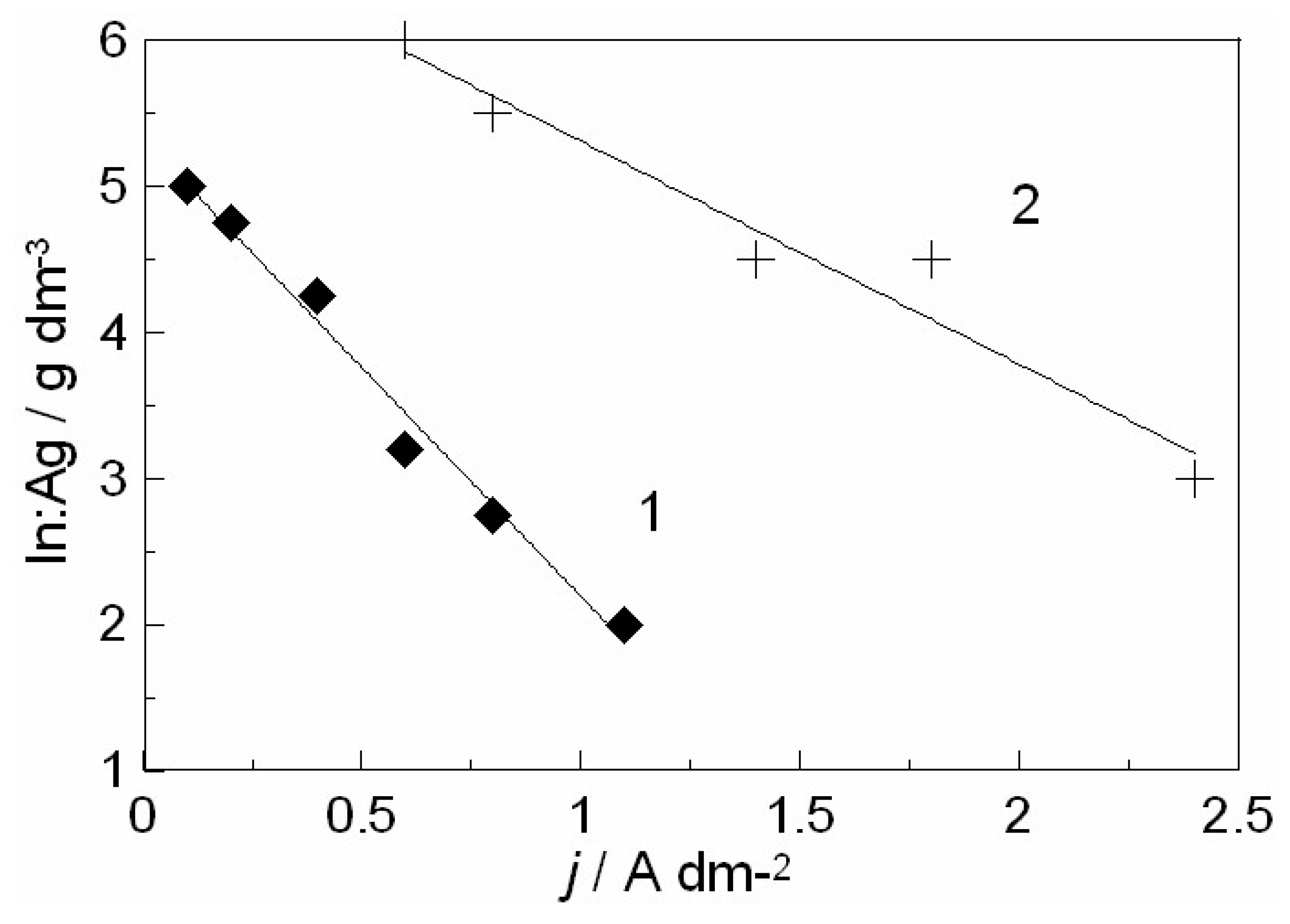
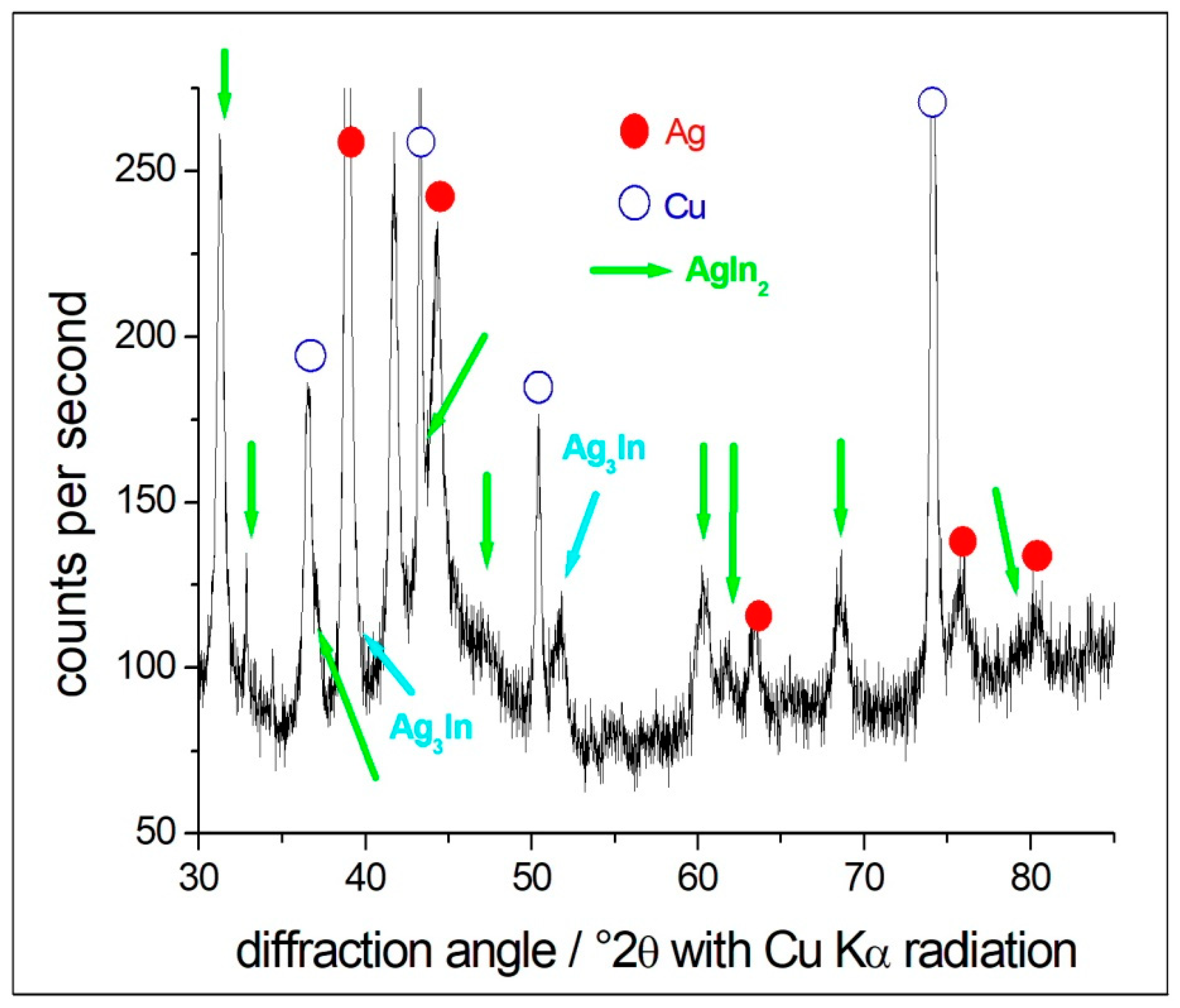
2.3.1. Ag-In Alloys

A spontaneously patterned Ag-In electrodeposit was obtained from an aqueous electrolyte of composition: KAg(CN)2 (Umicore, Schwäbisch Gmünd, Germany) 30 mM, InCl3 (Alfa Aesar, Kandel, Germany) 0.1 M, D(+)-glucose (Fluka) 0.1 M, KCN (Merck, Darmstadt, Germany) 0.5 M. The alloy was grown onto a Cu foil cathode (2 × 1 cm2) that was electrochemically degreased and pickled in H2SO4 20 vol % prior to electrodeposition. To avoid Ag displacement-plating, the Cu cathode was brought in contact with the electrolyte undercurrent. Alloy plating was carried out at room temperature in a 2-electrode cell using a large-area (20 cm2) platinized-titanium anode. Pattern formation can be controlled by appropriately adjusting: (i) the In3+/Ag+ ratio in the plating bath, (ii) the current density and (iii) the fluid dynamic conditions of the electrolyte. Figure 4 reports the experimental conditions ensuring pattern formation in stagnant (diamonds) and stirred (crosses, magnetic stirring at 50 rpm, 100 mL cell) electrolytes. The alloy was grown by electrodeposition at 0.5 A/dm2 for 2.5 h, yielding a coating thickness of ca. 40 μm. More experimental and theoretical details, as well as comprehensive reference to relevant literature, can be found in ref. [26]. The sample analyzed in this research (Figure 5) shows a double-spiral pattern with a spiral-core distance of ca. 0.5 mm and branch spacing of 0.15 mm. The sample exhibits a 3-phase crystallographic structure, featuring α−Ag-rich terminal solid solution (Figure 6; marked with red dots) and the Ag3In and AgIn2 intermetallics, as shown by the Powder Diffraction Files (PDF) Cards No: 29-0677 and No: 65-1552, respectively, in keeping with the literature [27,28]. The same phase structure was found in the single-spiral sample studied in [26]: the quantitative differences in phase composition and preferential orientations are compatible with differences in electrodeposition current density.
The photon energy employed was 652 eV, yielding an energy resolution of about 0.4 eV for imaging. The intrinsic surface sensitivity of soft-X ray photoelectron spectroscopy, enhanced by the grazing acceptance detection of SPEM (see Section 2.1 above), provides an effective probing depth limited to 1 nm, with dominating contribution from the top two atomic layers. Details on the image processing procedure are reported in the Supporting Information of ref. [26]. Ar+ bombardment (1.5 × 10⁻⁵ mbar Ar, 1–1.5 kV, sample current of 0.8 µA) erosion was employed for depth-profiling purposes; the ion beam was delivered at 45° with respect to the sample. Sequential sputtering periods were applied, corresponding to depths of 2, 4, 10, 20, 50, 65 and 90 nm, estimated according to standard models for sputtering depth ([29] and references therein): for full methodological and quantitative details, refer to ref. [26]. These sputtering steps effectively allow for monitoring of progressive depth variations in the alloy pattern. Possible sputter-induced roughening of the original surface topography [30] was monitored by AFM and found to be negligible and therefore to have no impact on the measured variations in the composition. Moreover, the evident chemical changes taking place in-depth demonstrate that intermixing and re-deposition of sputtered material are negligible.

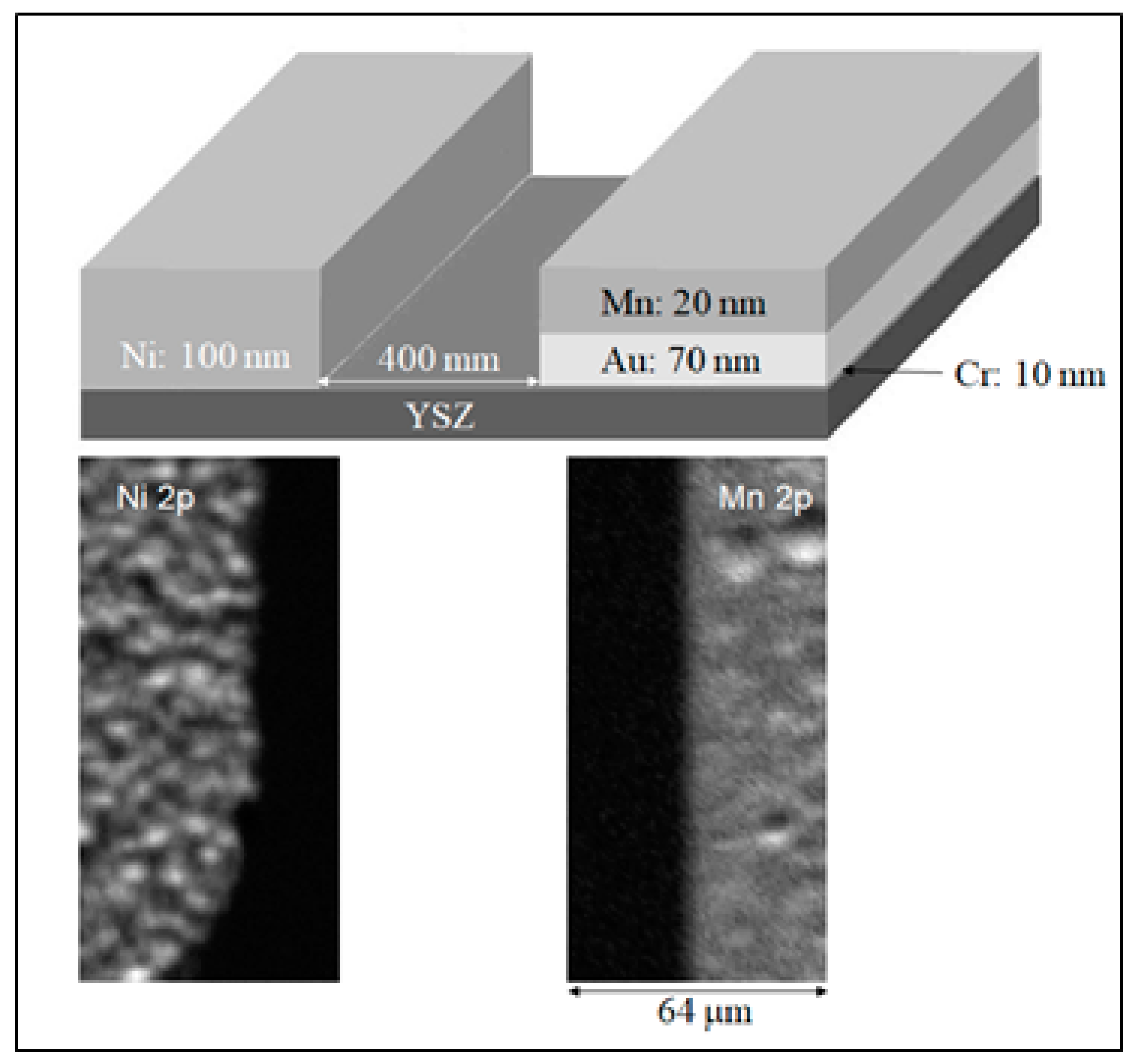
2.3.2. Mn-Ni SOFC at High Vacuum

For this experiment, we have used planar, YSZ(100)-supported cells with Ni and Au/Mn layers: the electrodes were fabricated by evaporating 100 nm thick Ni layers, and Au (70 nm)–Mn (20 nm) bi-layers grown onto a Cr adhesion buffer (10 nm): the cell scheme is depicted in Figure 7 (for details on fabrication, see, e.g., ref. [31]). Prior to measurements, the samples were subjected to Ar+ sputtering to remove contaminant layers introduced during fabrication, followed by annealing at 650 °C in 1 × 10⁻⁵ mbar O2 to restore the initial oxidation state of the materials. Electrochemical measurements were run with a PAR potentiostat. The cell was short-circuited through a potentiostat working in a ZRA (Zero-Resistance Ammetry) mode for simultaneous monitoring of the current response.
To optimize the photoemission yield of the main core levels, a photon energy of 1000 eV was set. As for all the experiments reported in this paper, a 5.0 purity grade of the gases was used.

2.3.3. LSM-NiO Single Chamber SOFC

The experiments on the single chamber SOFC were performed on (100)-oriented single crystal YSZ (ZrO2 stabilized with 9.5 % Y2O3) electrolyte on top of which a mixture of 50 wt % of LSM-YSZ (La0.8Sr0.2)0.95MnO3 and 50 wt % of (Y2O3)0.08(ZrO2)0.92 was used as cathode and a mixture of 60 wt % NiO and 40 wt % of (Y2O3)0.08(ZrO2)0.92 (Ni–YSZ) as anode. The LSM-YSZ and Ni-YSZ powder mixtures were blended with an organic vehicle and screen-printed on the electrolyte, forming two symmetrical rectangles separated by a gap of ∼ 1.5 mm and sintered at 1200 °C for 2 h. An Pt grid was also screen printed onto the electrodes and subsequently fired at 1100 °C for 30 min to provide a more uniform distribution of potentials and more robust electrical contact. The SC-SOFC experiments were carried out at 923 K with a CH4/O2 gas mixture with a volume ratio of 2/1, in conformity with the largest proportion of the available literature. A more detailed description of the sample preparation can be found in ref [32].
To optimize the photoemission yield of the main core levels a photon energy of 750 eV was set. In the results section of this paper, a collection of photoemission spectra and chemical maps will be shown; in most of the measurements, an overall energy resolution of 0.35 eV was set. The deconvolution of the spectra was performed using Doniach–Sunijch functions convoluted with Gaussians, following well-established procedures.
Electrochemical measurements have been carried out in a two-electrode configuration with a Versastat potentiostat.
The planar configuration, with anode and cathode on the same plane, is a classical SC-SOFC configuration also for practical applications (see, among others, the following reviews [33,34,35]). The relative arrangement of the electrodes in practical systems is often of the interdigitated type, by the main reason for this is the extent of the electrodes in larger devices and this has no impact on microkinetics. One could argue about the optimization of the inter-electrode distance, but this aspect is exclusively relevant if energetic optimization of the device is at stake. In electroanalytic terms, however, the contribution of the ohmic drop of an unoptimized electrolyte gap can be very easily separated from charge-transfer and mass-transport contribution by standard electrochemical measurements, such as electrochemical impedance spectrometry. Therefore, with a straightforward ohmic correction, all the electrokinetic information can be accurately retrieved. In particular, the link between electronic conditions and surface chemistry can be established with utmost accuracy with our device.

3. Results

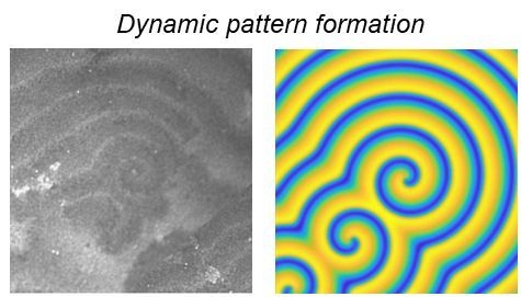
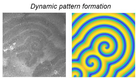
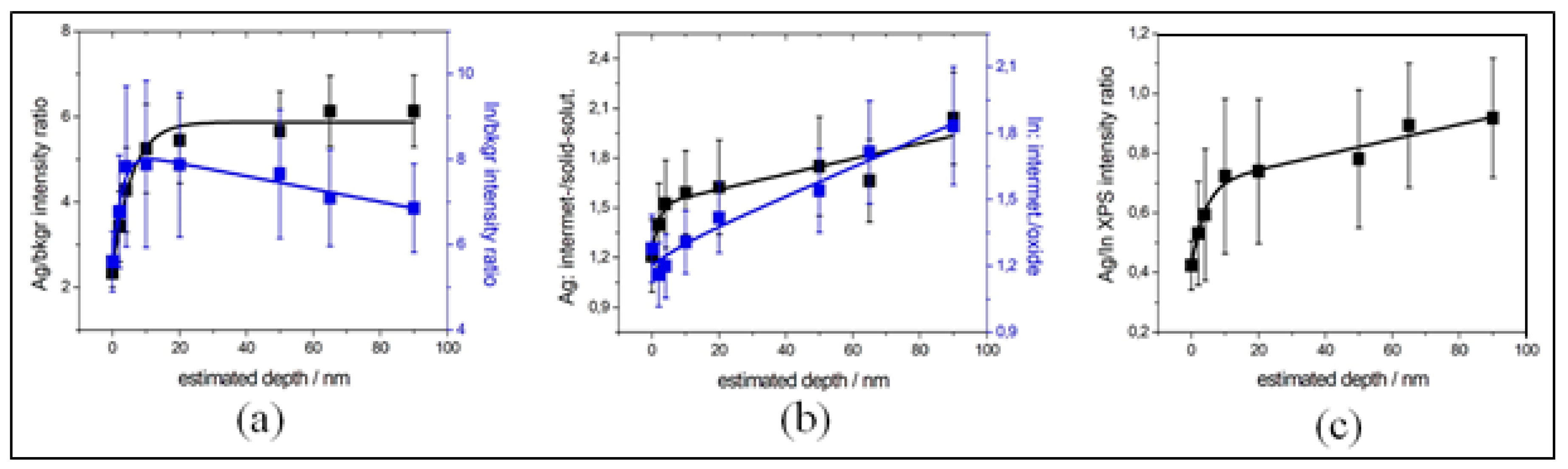
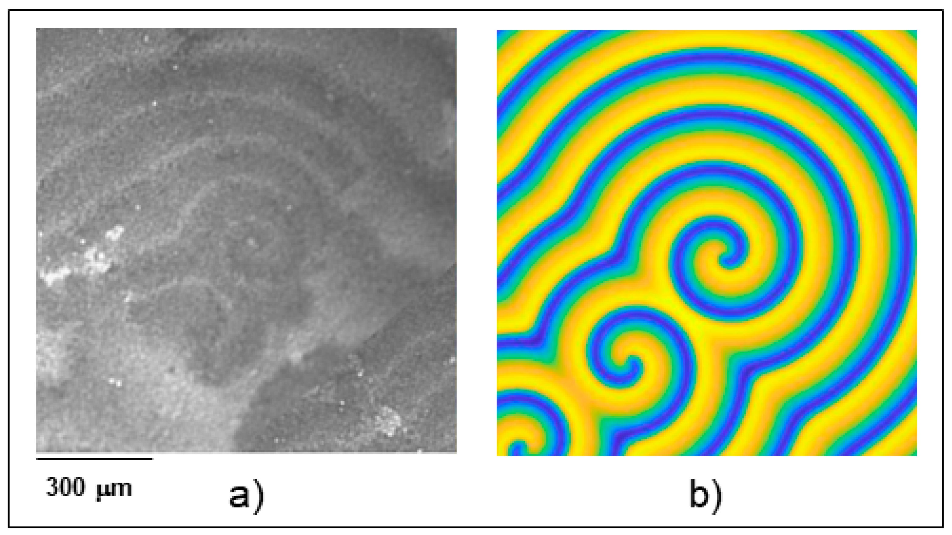
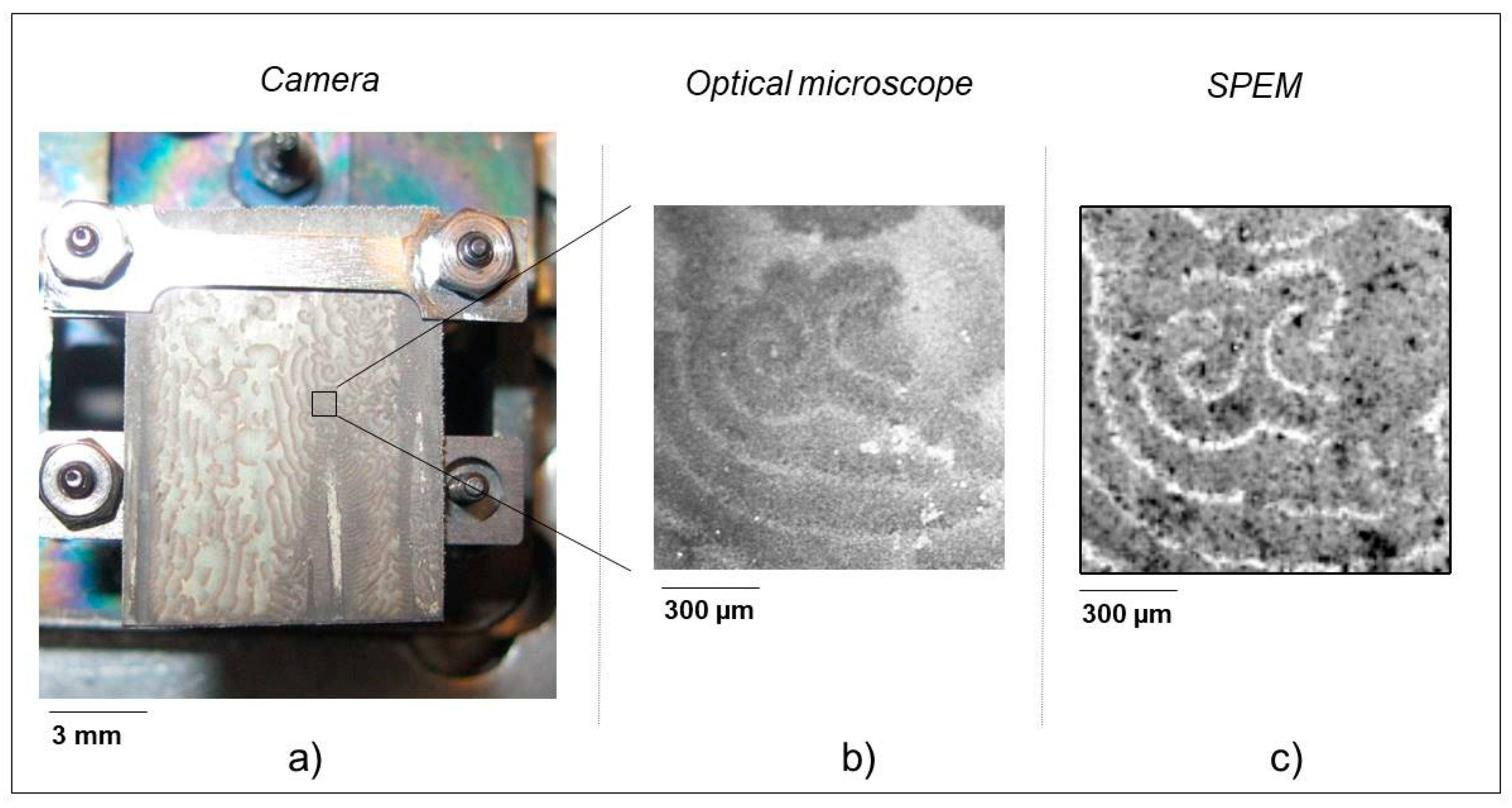
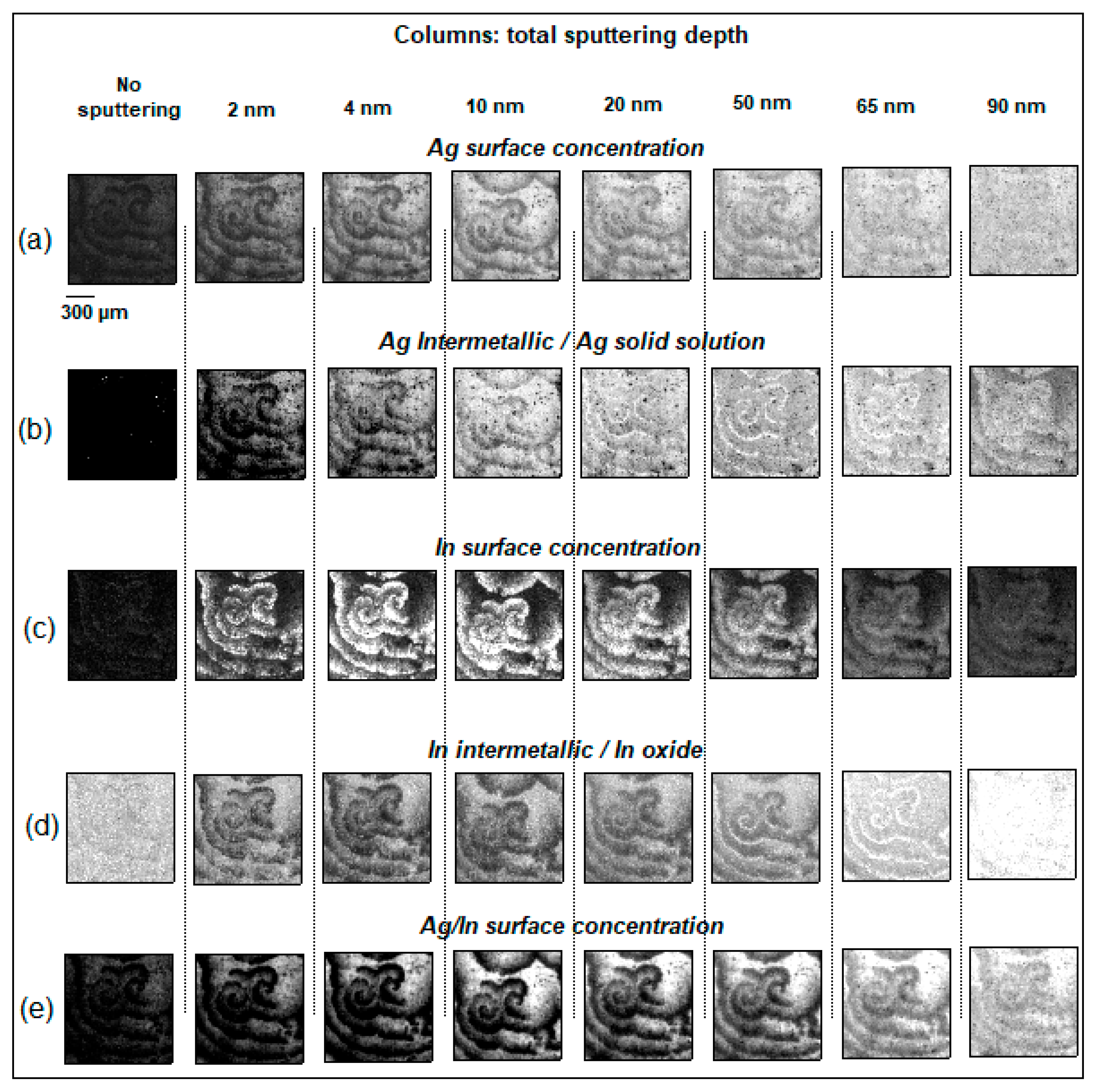
3.1. In-Depth Analysis of Ag-In Ex Situ Electrodeposited Alloys Exhibiting a Dynamic Pattern Formation Mechanism

A characteristic aspect of electrodeposited alloy patterns is that these structures can be imaged very precisely by visible-light microscopy, but exhibit a strikingly poor contrast in SEM, owing to their extreme surface-confinement. As proved in ref. [26,36], SPEM, owing to its high chemical-state sensitivity combined with surface sensitivity and lateral resolution, is the method of choice for unravelling the morphochemical details of electrodeposited alloy patterns. In view of completing and further validating the scenario set up in the two publications mentioned just above, in this study we have explored the 3D space elemental and chemical-state distribution of an Ag-In sample, fabricated under different conditions with respect to the one investigated in ref. [26]. Insight into the chemical speciation of Ag and In had been gained in the detailed study reported in ref. [26], were we disclosed that Ag is present in two chemical states: elemental (solid solution) and intermetallic, while In exhibits an oxidized and an intermetallic form. This chemical-state scenario has been confirmed in the analysis of the new sample and this information has been directly used for image processing of the Ag 3d and In 3d SPEM maps, with the method expounded in the Supporting Information of ref [26]. Briefly, the compositional inhomogeneity of the sample has been quantified by selecting the parts of the spectrum recorded in correspondence of each pixel of the image, representing one of the two components of the two key elements of the alloy. Figure 8 shows a representative selection of Ag 3d5/2 and In 3d5/2 SPEM images of the electrodeposited double-spiral, obtained by eroding the sample to the indicated depths. The maps depicted in Panels (a) and (c) were derived from the total intensity of the Ag and In 3d5/2 spectra and represent the spatial distribution of the Ag and In surface concentrations. Panels (b) and (d) show the Ag and In chemical maps, obtained by selecting the spectral regions representative of different chemical states. For Ag (Panel (b)) the contrast is due to the combination of intermetallic- and solid solution-type metallic states. Regarding In (Panel (d)), instead, contrast is determined by the distribution of In between Ag-In intermetallics and In3+ oxides/hydroxides. Coherently with our findings of ref. [26], it is clear that elemental contrast (Panels (a), (c)) tends to fade out rapidly in depth, while chemical-state contrast (Panels (b), (d)) is markedly more persisting. In addition, it is worth noting that the Ag and In elemental (Panels (a), (c)) and chemical-state distributions (Panels (b), (d)) are anticorrelated, in keeping with the surface concentration ratio distribution, imaged in Panel (e). Quantitative details, highlighting in-depth changes, can be more evidently pinpointed by averaging over space, as shown in Figure 9. Our results confirm the alloy electrodeposition mechanism proposed in [26] and further validates the mathematical DIB model of electrochemical pattern formation, recently developed in our group ([37,38] and references therein). More specifically, the present results provide additional support of the model capability of predicting complex spiral-based morphologies. Briefly, co-electrodeposition of In with Ag in amounts exceeding the solubility of the former element in the latter, gives rise to the formation of Ag-In intermetallics following a two-step process. Ag+ and In3+ are reduced to the elemental state, forming an α -Ag terminal solid solution together with Ag-In intermetallics, but simultaneously basic In3+ salts precipitate at the electrode-electrolyte interface. The basic-salt film, in turn, can be electro-reduced forming fresh elemental In that can react with α-Ag to form more intermetallic. This two-step process effectively explains why In3+ oxi-hydroxides can be found at the alloy surface, but they are absent in the bulk of the layer. As far as pattern formation is concerned, the DIB model provides a simple framework for the rationalization of this phenomenon, in that it predicts that the coupling of electrodeposit morphology with adsorption of an electroactive intermediate can give rise to the formation of dynamic patterns, among which double-spirals [39]. SPEM maps provide factual spectroscopic evidence of the presence of adsorbed In3+ electroactive intermediates and of their organization in a typical pattern. In addition, a set of DIB-model parameters can be identified, yielding a computed pattern with a remarkably good matching between the theoretical map and the experimental pattern (Figure 10). The difference in the numerical values of the parameters that correspond to the double-spiral pattern with respect to those found for the single spiral studied in [26], is coherent with the different current-density values employed for the growth of the two alloys (for details on the correspondence between model parameters and experimental variables, see [40]).

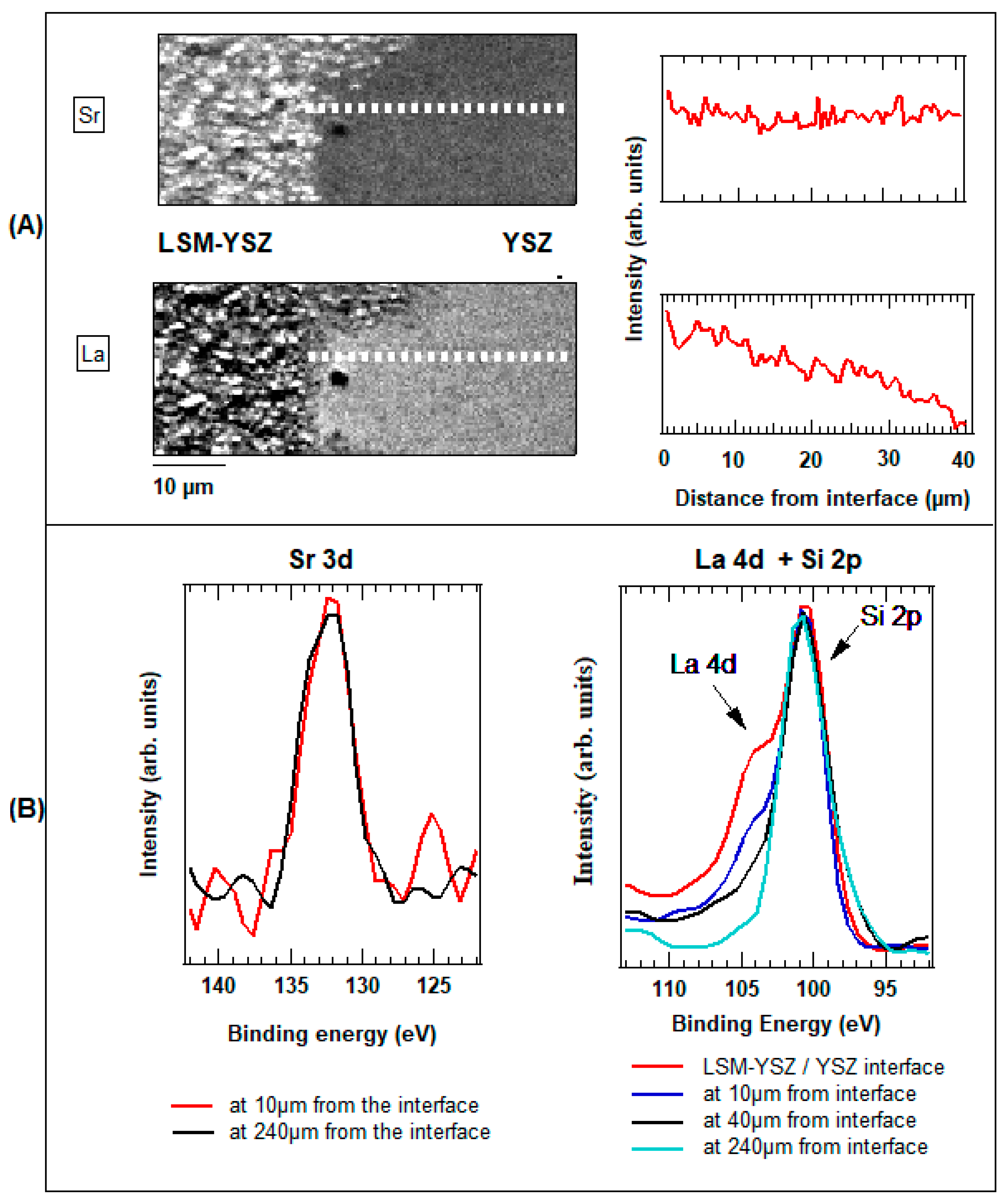
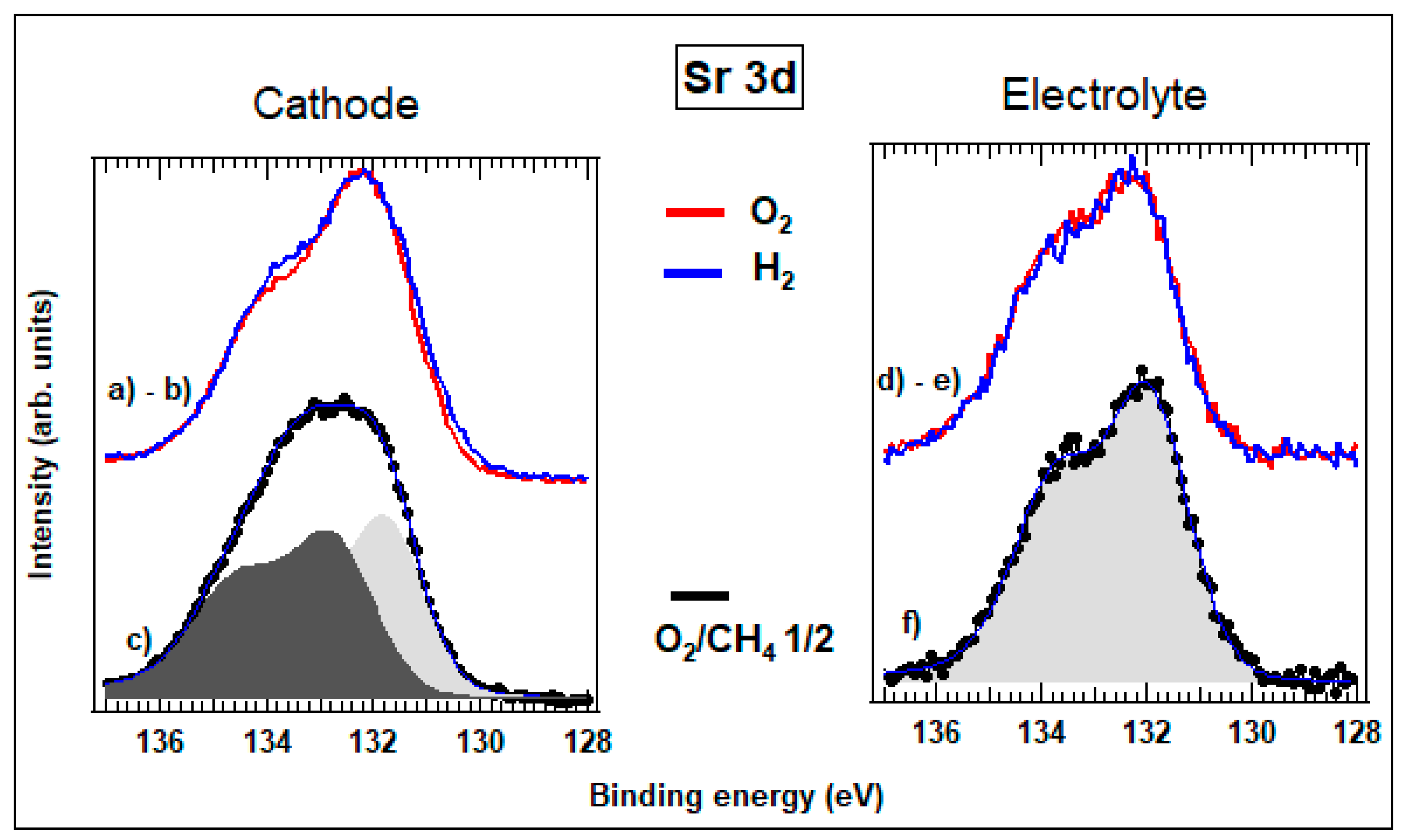
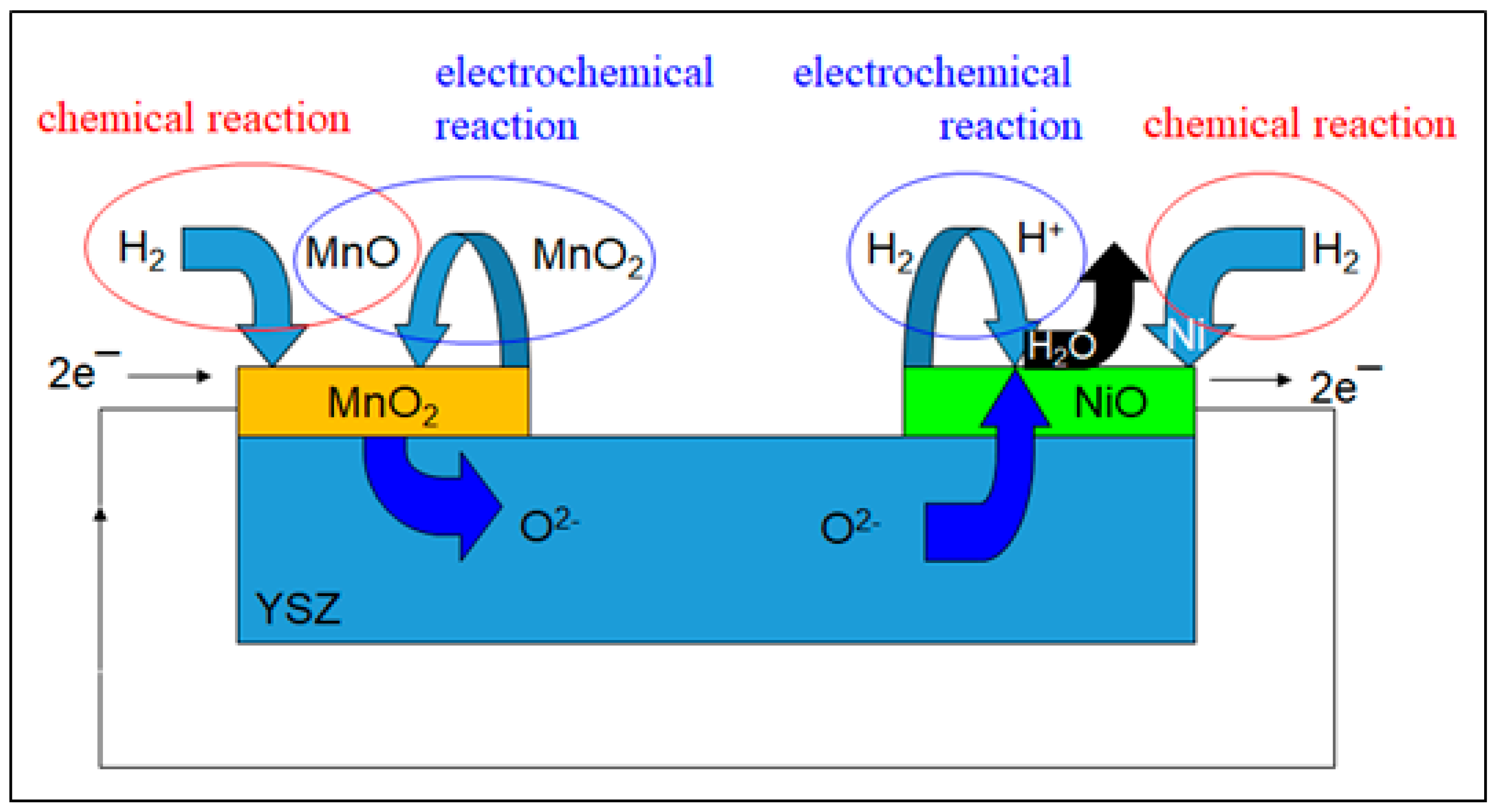
3.2. Spectromicroscopy Analysis of Electrochemical Processes at the Electrodes of a Self-driven Solid Oxide Fuel Cell

The present section contributes to the scantily covered field of in situ SPEM studies of self-driven electrochemical systems, in which chemical energy is spontaneously converted into electrical energy. In situ studies of self-driven fuel cells and batteries, though more difficult than those of externally-driven systems such as symmetric cells or cells with a single electrode running the real reaction of the energetic device, is notably important because the couplings between the anodic and cathodic phenomena are known to play a crucial role for the efficiency and durability of devices for electrochemical energetics. In the present study, we investigate a cell with a solid cathodic reagent, MnO2, and an anodic gas, H2, reacting at a Ni/NiO electrocatalyst. In particular, we compare operating conditions with active gas pressures in the high vacuum and NAP ranges.
Sample annealing in 10−5 mbar of O2 at 923 K in the SPEM chamber, resulted in the oxidation of the starting materials to NiO and MnO2 that, by exposure to different pressures of H2, can transform into Ni and MnO, generating different redox couples at the two electrodes, yielding in turn electrical power, according to the scheme of Figure 11. The electrokinetics of the system was followed with transient experiments consisting in switching from O2 10−5 mbar to H2 10−5 and 1 mbar, and recording time-dependent spectra and current time-series (Figure 12). In order to emphasize the current response, the cell was short-circuited and the current was measured with a ZRA. Curve (A) in Figure 12 shows a representative transient corresponding to switching from 10−5 mbar O2 to 10−5 mbar H2. In keeping with the thermodynamic analysis of ref. [41], H2 is oxidized to H2O and MnO2 is reduced to MnO, giving rise to the electrochemical reaction indicated in Figure 12, whereby O2− is transported through the electrolyte. In correspondence, also Ni forms, enhancing the H2 oxidation rate, as witnessed by the progressive rise in current, in keeping with the literature [42]. Curve (B) is obtained by switching from 10−5 mbar O2 to 1 mbar H2. In these conditions, on the one hand, the electrochemical reaction is faster, but, on the other hand, also the chemical reduction of MnO2 is anticipated, resulting in a progressive decrease of the cell current.
Panels (A) and (B) of Figure 13 report representative sequences of Ni 2p µXPS spectra acquired after having switched the gas ambient from 10-5 mbar O2 to 10−5 and 1 mbar H2, respectively. Replicated experiments confirm in detail the observed kinetics. Ni in the initial state is fully oxidized and a progressive reduction can be noticed, that is notably faster in the case of the lower-pressure experiment. The reduction rates are summarized in Panel (C). Panel (D) reports the Mn 2p µXPS spectra acquired for the initial and final states of the cathode at the two H2 pressures investigated: formation on MnO can be clearly assessed from the characteristic satellite structure [43]. Coherently with the recorded cell-currents and compatibly with the thermodynamic framework of ref. [41], at high pressure, the electrochemical reaction with H2 oxidation at NiO and MnO2 reduction to MnO is faster than the chemical Ni reduction and for this reason NiO is stabilized at short times. At low pressure instead, the chemical reduction of Ni is favoured, resulting in a progressive enhancement of the electrocatalytic performance of the anode.

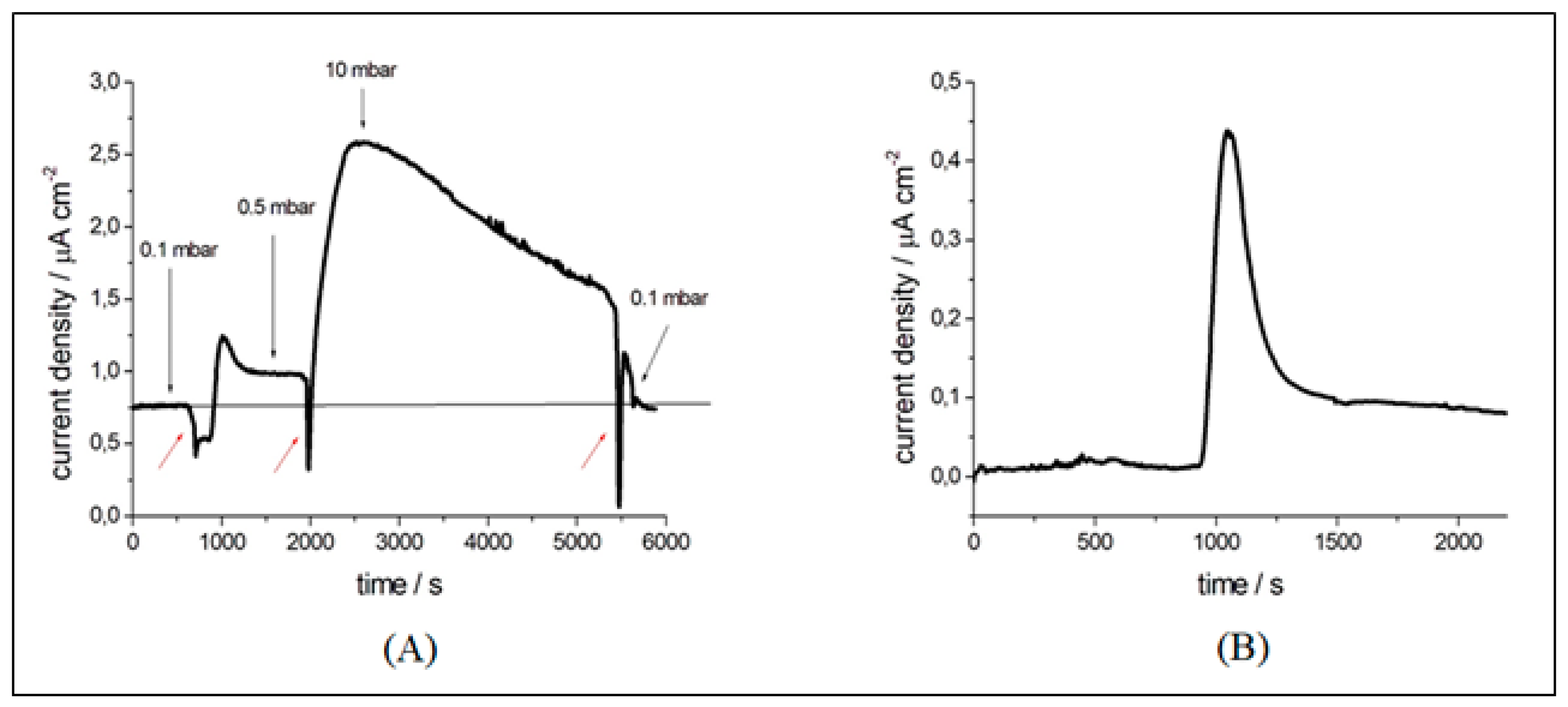
3.3. Operando Characterization of a Single-chamber Solid Oxide Fuel Cell at Near-ambient Pressure

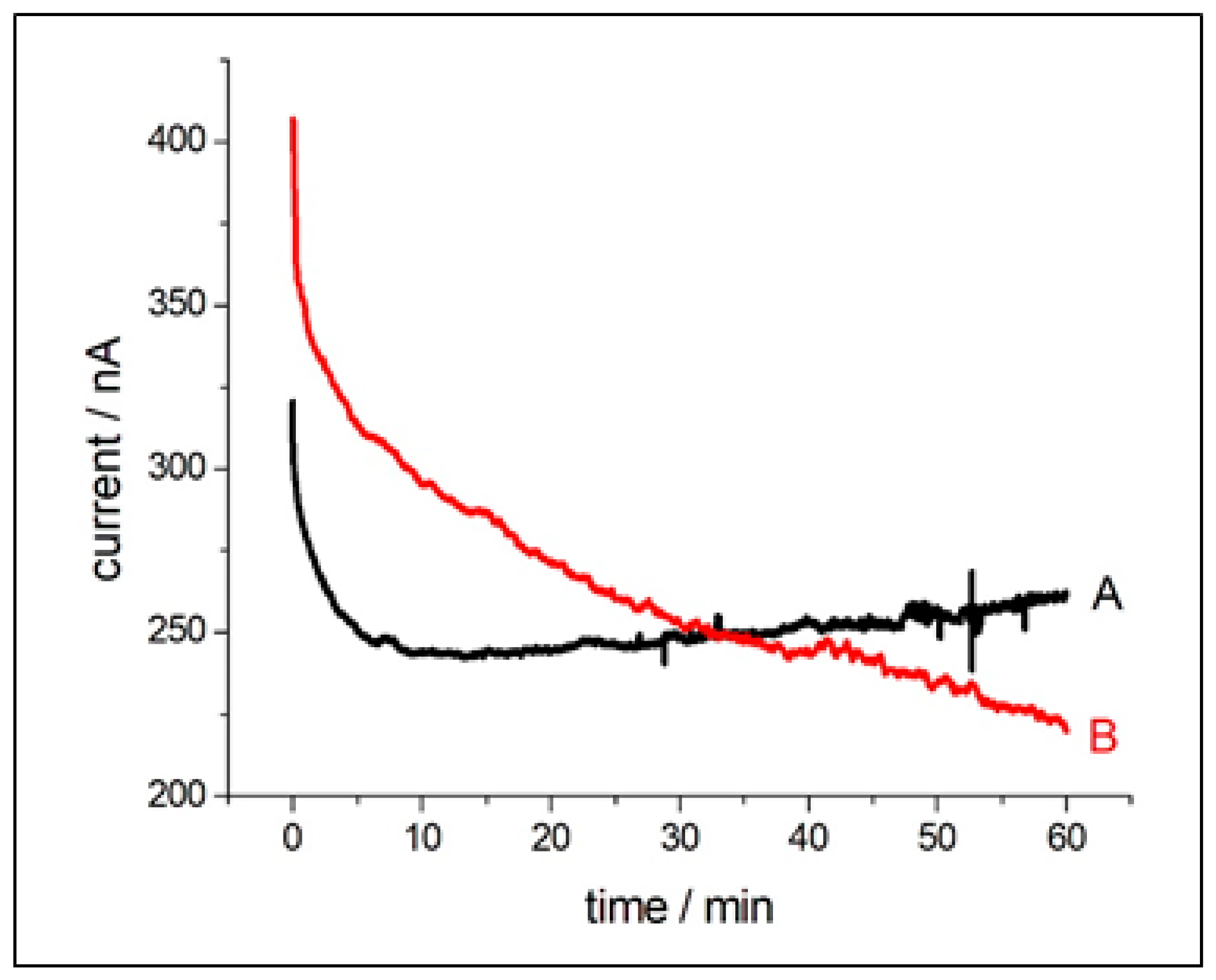
3.3.1. Electrochemical Measurements

Since limited literature information is available on the performance of SC-SOFC at the pressures of interest for APXPS, preliminarily to operando spectroscopy, we carried out calibration work in a range of vacuum conditions spanning the interval including the actual operating conditions and slightly higher ones, that allow the achievement of electrochemical responses that match the ones obtained at conventional working pressures. In Figure 14 we report a representative selection of current transients obtained by short-circuiting the cell in the reactive gas mixture: the actual operating condition during SPEM. More information including pressure-dependent open-circuit potentials and electrochemical impedance spectrometry can be found in ref. [26]. We have chosen to operate the SC-SOFC under short-circuited conditions because, on the one hand, even though the current that can be drawn from the device is rather low, it can be measured accurately and demonstrates the correct SOFC operation and, on the other hand, since short-circuit represents the most aggressive condition, successful operation in this condition is an a fortiori proof of the feasibility of the approach. These experiments consisted in measuring the cell current with the ZRA method in CH4/O2 = 2/1 mixtures of defined pressure. One can observe that a sudden current surge is followed by a relaxation, the rate of which negatively correlates with the pressure. After the transient, the current tends to a well-defined steady-state: this allows to run NAP-SPEM experiments under perfectly controlled electrochemical conditions.

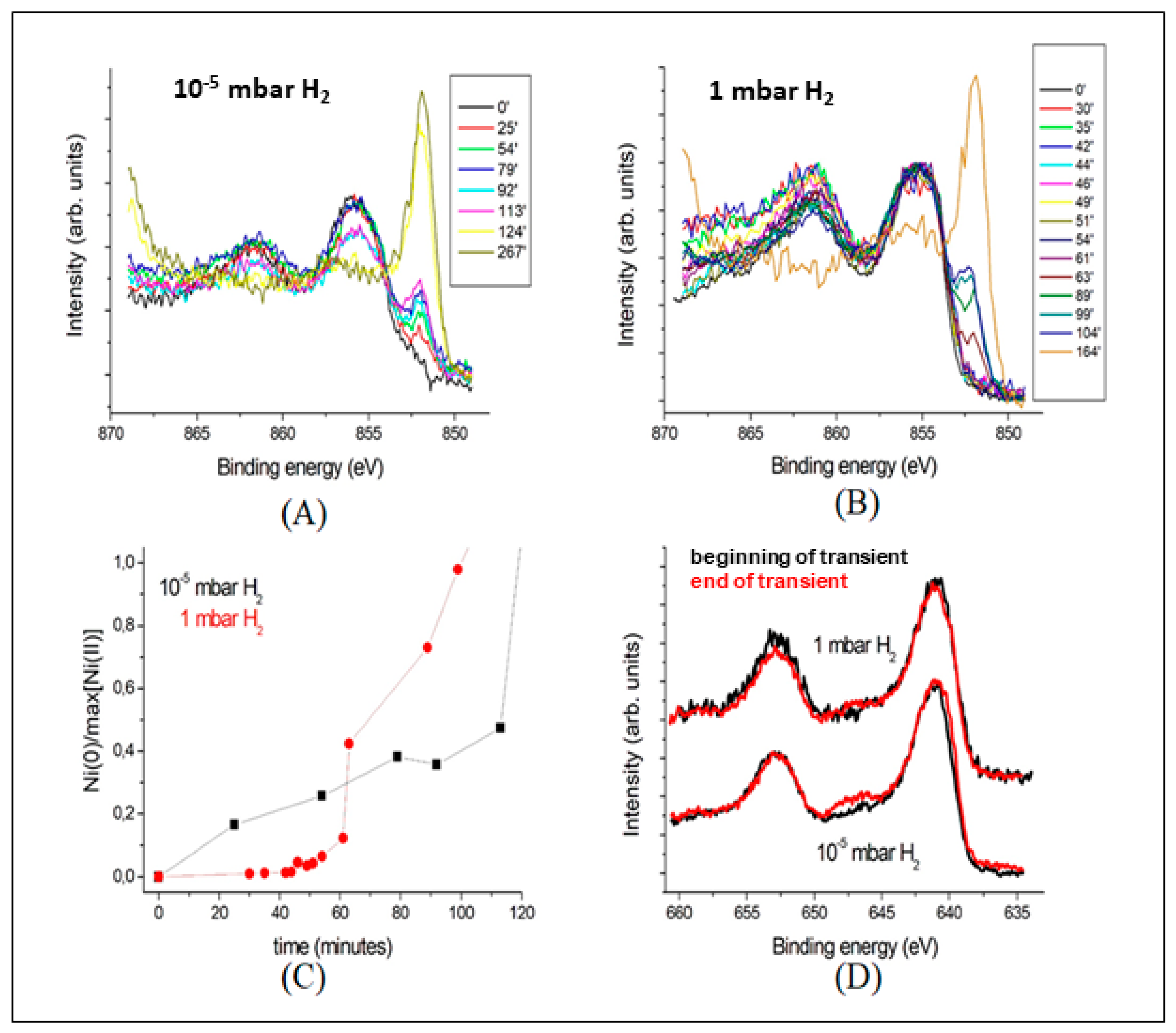
3.3.2. Spatially Resolved Photoemission Measurements at Near Ambient Pressure

In order to prove the validity of our approach as robustly as possible, we have decided to carry out operando XPS concentrating on the cathode of the NiO/YSZ/LSM SC-SOFC, since the chemical state of the elements of this perovskite is far less sensitive to electrochemically-induced changes in comparison with Ni [41]. In the SPEM, the cell temperature was set to 923 K for the whole measurement time. To avoid any reduction of the electrode/electrolyte surface due to the combination of vacuum/high temperature, in the stand-by periods between electrochemical measurements, a partial pressure of 5 × 10⁻² mbar of O2 was introduced in the NAP-Cell. In these conditions, we have measured several μXPS survey and high-resolution spectra as well as SPEM maps in different locations to probe the chemical composition of the cathode and of the interface region and its morphology of pristine cells. In addition to the main constituents of the cathodic/electrolyte material (La, Sr, Mn, Zr, Y, O) we also assessed the presence of two impurities: C and Si, the latter being typical for YSZ [42]. Figure 15 reports a representative selection of maps at the Sr 3d and La 4d energies (Panel (A)) and µXPS spectra (Panel (B)) in the region across the interface between the LSM-YSZ patch (left) and the YSZ electrolyte (right). These elemental maps show a clear topographic contrast in the cathode region, highlighting micrometric and submicrometric granular morphology, combined with evident chemical contrast. In addition, signal from Sr and La can be detected inside the electrolyte, proving diffusion of these elements into the YSZ region. Differently from Sr and La, Mn remains strictly confined to the cathode region. At the right of Panel (A), we show intensity profiles for Sr 3d and La 4d signal extracted from the SPEM maps along the dotted lines and in Panel (B) we report μXPS spectra measured at different positions along the same line, up to 240 μm from the electrode/electrolyte interface. The La 4d spectrum is partly overlapping the Si 2p one, that provides a convenient internal reference for relative intensity variations of this perovskite component. The spatial dependence of the Sr and La signal shows that the surface coverage of YSZ with Sr is constant in the investigated zone, while a La gradient can be appreciated, highlighting a difference in the surface diffusion coefficients of these two components of the cathodic material on the electrolyte. In this work, we concentrated on the evolution of the cathode elements in SC-SOFC ambient and under electrochemical operating conditions. In particular, we carried out a fine analysis of the La 4d, Zr 3d, O 1s and Mn 2p core levels, acquired on different grains of the cathode, as well as in representative locations of the electrolyte, in the following ambients: (i) 0.05 mbar O2; (ii) 0.1 mbar H2 and (iii) 0.1 mbar CH4/O2 = 2/1. The electrochemical conditions tested were: (a) OCP in all three ambients, (b) short-circuited cell in ambient (iii). Ambient (iii) is the reactive gas mixture employed for self-driven SC-SOFC operation (for details, see [26,41]); as hinted-at above, ambient (i) was used to preserve the original chemistry of the cell components in stand-by conditions between electrochemical measurements and ambient (ii) was set for 1 h before starting the SC-SOFC operation in order to activate the NiO anode [38]. Briefly, detailed analysis of the La 4d, Zr 3d and Mn 2p core level spectra acquired on different grains of the cathode and on the electrolyte under all investigated conditions, did not exhibit any effect either of the ambient or of the electrochemical polarization. These spectra showed the typical binding energies and spectral shape reported in the literature for similar materials [43,44,45,46] and the only differences were in the intensities, as a result of the heterogeneous stoichiometry of the LSM-YSZ grains. Instead, the Sr 3d line exhibited chemical-state sensitivity to the gas ambient: specifically, spectral changes have been found in H2 and CH4/O2 ambients, as detailed below. It is worth noting that the chemical state of Sr in SOFC materials has been investigated by ex situ XPS in some detail in the literature [44,46,47,48]. Briefly, on the one hand, Sr has been described in La-Sr perovskites with transition metals and, on the other hand, as a species diffused on YSZ. The former state—characterized by an XPS spectrum with peaks at BEs between 131.4 and 132.5 eV—, corresponds to the perovskite lattice. The latter state—exhibiting peaks at BEs between 132.8 and 133.8 eV— denotes the separation of a secondary oxidic phase. In the cases reported in the literature, these two prototypical chemical states are typically found in combination within the probed volume.
In our experiments carried out in H2 atmosphere, a slight, but well-defined spectral change in the low BE tail of Sr spectra located on the cathode patch was found during the change from O2 to H2 atmosphere, while the same element, in the form expressed when diffused into the electrolyte region, did not respond to the change (Figure 16, spectra a), b), d) and e)). This chemical change of Sr in LSM cannot be reliably accounted for on the basis of the available literature, but can be justified in terms of partial reduction.
As anticipated in ref. [26], the introduction of SC-SOFC CH4/O2 2/1 gas feed in the NAP-Cell brings about a notable, irreversible change in the Sr 3d spectrum measured at the cathode (Figure 16, spectrum (c)), while no changes are found in Sr diffused onto the electrolyte patch (Figure 16, spectrum (f)). The spectral change found in the cathode region occurs at OCP and it is not further modified by applying electrochemical polarization within the range of self-driven SC-SOFC operation. The µXPS spectrum recorded in the cathode region exhibits a strong surface contribution, while that measured on the electrolyte patch can be entirely accounted for by lattice Sr. The observed irreversible surface segregation of Sr by XPS is in keeping with literature results reporting, on the one hand, the formation of a SrO surface phase by crystallographic means [49] and, on the other hand, electrocatalytic degradation due to blocking of the ORR active sites [50].

4. Conclusions

Scanning photoelectron spectromicroscopy has undergone a fast development at the third-generation synchrotron light sources, becoming a true microscopic tool for probing material properties, mainly at their surface. In the field of electrochemistry this approach has been proved capable of following morphological and chemical effects occurring at surfaces and interfaces. The present paper reviews three different experiments showing how SPEM can overcome the “material” and “pressure” gaps in the characterization of electrochemical surfaces. In the first experiment the fascinating spatiotemporal patterns formed during an ex situ electrodeposition of an Ag-In alloy has been investigated. A depth profile mapping of the distribution of the chemical states of Ag and In with high spatial and spectral resolution has been performed providing a 3D frame of the patterns. The experimental data perfectly match the mathematical predictions of the DIB model of electrochemical pattern formation.
The other two cases reported in the manuscript deal with the analysis of electrochemical processes at the electrodes of solid oxide fuel cells. In the first case, an in situ study of a self-driven cell was performed. The cell was formed by a solid cathodic material, MnO2, and a mixture of Ni/NiO as anode. The system was analyzed at high vacuum and near ambient environmental pressure conditions. The main achievement is that, coherently with the recorded cell currents at high H2 pressure, its oxidation at NiO and the corresponding MnO2 reduction to MnO is faster than the chemical Ni reduction and for this reason, NiO is stabilized at short times. At low pressure instead, the chemical reduction of Ni is favoured, resulting in a progressive enhancement of the electrocatalytic performance of the anode.
In the last experiment, we have shown an operando analysis of a single-chamber solid oxide fuel cell at near ambient pressure regime by using a unique specially designed setup which extends the traditional capabilities of scanning photoemission microscopes in the ultra-high and high-vacuum regimes to more realistic conditions of environmental pressure. The response of the cathodic site of a NiO/YSZ/LSM SC-SOFC exposed to O2, H2 and a mixture of CH4 and O2 showed a chemical-state sensitivity of Sr: a well-defined spectral change in the low BE tail of Sr spectra located on the cathode patch was found during the change from O2 to H2 atmosphere, while the same element, when diffused into the electrolyte region, did not respond to the same change. This chemical change of Sr in LSM cannot be reliably accounted for on the basis of the available literature, but can be justified in terms of partial reduction. Moreover, the CH4/O2 2/1 gas feed brings about a notable, irreversible change in the Sr 3d spectrum measured at the cathode, while no changes are found in Sr diffused onto the electrolyte patch.
We believe the reported examples demonstrate the great potential of SPEM to gain insight into electrochemical and chemical processes taking place in energy conversion and other systems, which can guide the design of next-generation devices with improved performance.

Author Contributions

D.K. prepared the single-chamber SOFC test samples. All authors characterized the samples, revised and edited the manuscript.

Funding

The research leading to these results has received funding from the European Community’s Seventh Framework Programme (FP7/2007-2013) under grant agreement nº 312284 and the European Community’s Horizon 2020 Framework Programme under grant agreement nº 730872. The author D.K. acknowledges the financial support from the Slovenian Research Agency (research core funding No. P2-0105).

Conflicts of Interest

The authors declare no conflict of interest.

References

  1. Nasirpouri, F. An Overview to Electrochemistry. In Electrodeposition of Nanostructured Materials; Springer Series in Surface Science 62; Springer: Berlin, Germany, 2017; Volume 62, pp. 43–73. [Google Scholar]
  2. Buckley, D.N.; O’Dwyer, C.; Quill, N.; Lynch, R.P. Electrochemical energy storage. In Energy Storage Options and Their Environmental Impact; Hester, R.E., Harrison, R.M., Eds.; The Royal Society of Chemistry: London, UK, 2019; pp. 115–149. [Google Scholar]
  3. Lin, F.; Liu, Y.; Yu, X.; Cheng, L.; Singer, A.; Shpyrko, O.G.; Xin, H.L.; Tamura, N.; Tian, C.; Weng, T.-C.; et al. Synchrotron X-ray Analytical Techniques for Studying Materials Electrochemistry in Rechargeable Batteries. Chem. Rev. 2017, 117, 13123–13186. [Google Scholar]
  4. Margaritondo, G.; Cerrina, F. Overview of soft-X-ray photoemission spectromicroscopy. Nuclear Instrum. Methods A 1990, 191, 26–35. [Google Scholar] [CrossRef]
  5. Ade, H.; Kirz, J.; Hulbert, S.; Johnson, E.; Anderson, E.; Kern, D. Scanning photoemission microscopy with synchrotron radiation. Vac. Sci. Technol. 1991, A9, 1902. [Google Scholar]
  6. Günther, S.; Kaulich, B.; Gregoratti, L.; Kiskinova, M. Photoelectron microscopy and applications in surface and materials science. Prog. Surf. Sci. 2002, 70, 187–260. [Google Scholar] [CrossRef]
  7. Amati, M.; Barinov, A.; Feyer, V.; Gregoratti, L.; Al-Hada, M.; Locatelli, A.; Mentes, T.O.; Sezen, H.; Schneider, C.M.; Kiskinova, M. Photoelectron microscopy at Elettra: Recent advances and perspectives. J. Electron. Spectrosc. Relat. Phenom. 2018, 224, 59–67. [Google Scholar] [CrossRef]
  8. Horiba, K.; Nakamura, Y.; Nagamura, N.; Toyoda, S.; Kumigashira, H.; Oshima, M.; Amemiya, K.; Senba, Y.; Ohashi, H. Scanning photoelectron microscope for nanoscale three-dimensional spatial-resolved electron spectroscopy for chemical analysis. Rev. Sci. Instrum. 2011, 82, 113701-1. [Google Scholar] [CrossRef]
  9. Bozzini, B.; Amati, M.; Gregoratti, L.; Kazemian, M.; Prasciolu, M.; Tondo, E.; Trygub, A.L.; Kiskinova, M. In Situ Electrochemical X-ray Spectromicroscopy Investigation of the Reduction/Reoxidation Dynamics of N-Cu Solid Oxide Fuel Cell Anodic Material in Contact with a Cr Interconnect in 2 × 10⁻⁶ mbar O2. J. Phys. Chem. C 2012, 116, 7243–7248. [Google Scholar] [CrossRef]
  10. Huber, A.; Falk, M.; Rohnke, M.; Luerssen, B.; Gregoratti, L.; Amati, M.; Janek, J. In situ study of electrochemical activation and surface segregation of the SOFC electrode material La0.75Sr0.25Cr0.5Mn0.5O3+/-δ. Phys. Chem. Chem. Phys. 2012, 14, 751–758. [Google Scholar] [CrossRef]
  11. Backhaus-Ricoult, M.; Adib, K.; Work, K.; Badding, M.; Ketcham, T.; Amati, M.; Gregoratti, L. In-situ scanning photoelectron microscopy study of operating (La,Sr)FeO3-based NOx-sensing surfaces. Solid State Ion. 2012, 225, 716–726. [Google Scholar] [CrossRef]
  12. Jirgensen, A.; Esser, N.; Hergenrçder, R. Near ambient pressure XPS with a conventional X-ray source. Surf. Interface Anal. 2012, 44, 1100–1103. [Google Scholar] [CrossRef]
  13. Bluhm, H.; Havecker, M.; Knop-Gericke, A.; Kiskinova, M.; Schlögl, R.; Salmeron, M. In Situ X-ray Photoelectron Spectroscopy Studies of Gas-Solid Interfaces at Near-Ambient Conditions. MRS Bull. 2007, 32, 1022–1030. [Google Scholar] [CrossRef]
  14. Crumlin, E.J.; Bluhm, H.; Liu, Z. In situ investigation of electrochemical devices using ambient pressure photoelectron spectroscopy. J. Electron. Spectrosc. Relat. Phenom. 2013, 190, 84–92. [Google Scholar] [CrossRef]
  15. Starr, D.E.; Liu, Z.; Hävecker, M.; Knop-Gericke, A.; Bluhm, H. Investigation of solid/vapor interfaces using ambient pressure X-ray photoelectron spectroscopy. Chem. Soc. Rev. 2013, 42, 5833–5857. [Google Scholar] [CrossRef]
  16. Crumlin, E.J.; Liu, Z.; Bluhm, H.; Yang, W.L.; Guo, J.H.; Hussain, Z. X-Ray Spectroscopy of Energy Materials under in Situ/Operando Conditions. J. Electron. Spectrosc. Relat. Phenom. 2015, 200, 264–273. [Google Scholar] [CrossRef]
  17. Takagi, Y.; Uruga, T.; Tada, M.; Iwasawa, Y.; Yokoyama, T. Pressure Hard X-ray Photoelectron Spectroscopy for Functional Material Systems as Fuel Cells under Working Conditions. Acc. Chem. Res. 2018, 51, 719–727. [Google Scholar] [CrossRef]
  18. Favaro, M.; Valero-Vidal, C.; Eichhorn, J.; Toma, F.M.; Ross, P.N.; Yano, J.; Liu, Z.; Crumlin, E.J. Elucidating the alkaline oxygen evolution reaction mechanism on platinum. J. Mater. Chem. A 2017, 5, 11634–11643. [Google Scholar] [CrossRef]
  19. Lichterman, M.F.; Richter, M.H.; Hu, S.; Crumlin, E.J.; Axnanda, S.; Favaro, M.; Drisdell, W.; Hussain, Z.; Brunschwig, B.S.; Lewis, N.S.; et al. An electrochemical, microtopographical and ambient pressure X-ray photoelectron spectroscopic investigation of Si/TiO2/Ni/Electrolyte Interfaces. J. Electrochem. Soc. 2016, 163, H139–H146. [Google Scholar] [CrossRef]
  20. Sezen, H.; Alemán, B.; Amati, M.; Dalmiglio, M.; Gregoratti, L. Spatially Resolved Chemical Characterization with Scanning Photoemission Spectromicroscopy: Towards Near-Ambient-Pressure Experiments. ChemCatChem 2015, 7, 3665–3673. [Google Scholar] [CrossRef]
  21. Amati, M.; Abyaneh, K.M.; Gregoratti, L. Dynamic High Pressure: A novel approach toward near ambient pressure photoemission spectroscopy and spectromicroscopy. J. Instrum. 2013, 8, T05001. [Google Scholar] [CrossRef]
  22. Gregoratti, L.; Barinov, A.; Benfatto, E.; Cautero, G.; Fava, C.; Lacovig, P.; Lonza, D.; Kiskinova, M.; Tommasini, R.; Mahl, S. 48-Channel electron detector for photoemission spectroscopy and microscopy. Rev. Sci. Instrum. 2004, 75, 64–68. [Google Scholar] [CrossRef]
  23. Miller, D.R. Atomic and Molecular Beam Methods, 1st ed.; Oxford University Press: Oxford, UK, 1988. [Google Scholar]
  24. Soukhanovskii, V.A.; Kugel, H.W.; Kaita, R.; Majeski, R.; Roquemore, A.L. Supersonic gas injector for fueling and diagnostic applications on the national spherical torus experiment. Rev. Sci. Instrum. 2004, 75, 4320–4323. [Google Scholar] [CrossRef]
  25. Piseri, P.; Podestà, A.; Barborini, E.; Milani, P. Production and characterization of highly intense and collimated cluster beams by inertial focusing in supersonic expansions. Rev. Sci. Instrum. 2001, 72, 2261–2267. [Google Scholar] [CrossRef]
  26. Bozzini, B.; Amati, M.; Dobrovolska, T.; Gregoratti, L.; Krastev, I.; Sgura, I.; Taurino, A.; Kiskinova, M. Depth-dependent scanning photoelectron microspectroscopy unravels the origin of dynamic pattern formation in alloy electrodeposition. J. Phys. Chem. C 2018, 112, 15996–16007. [Google Scholar] [CrossRef]
  27. Dobrovolska, T.; Jovic, V.D.; Jovic, B.M.; Krastev, I. Phase Identification in Electrodeposited Ag-In Alloys by ALSV technique. J. Electroanal. Chem. 2007, 611, 232–240. [Google Scholar] [CrossRef]
  28. Dobrovolska, T.; Beck, G.; Krastev, I.; Zielonka, A. Phase Composition of Electrodeposited Silver-Indium Alloys. J. Solid State Electrochem. 2008, 12, 1461–1467. [Google Scholar] [CrossRef]
  29. Briggs, D.; Seah, M.P. Practical Surface Analysis, Auger and X-ray Photoelectron Spectroscopy, 2nd ed.; Wiley: Chichester, UK, 1990; Volume 1. [Google Scholar]
  30. Bozzini, B. Effect of Sputter-Induced and other Roughness on Auger Electron Intensities. Il Vuoto 1997, 26, 18–29. [Google Scholar]
  31. Bozzini, B.; Amati, M.; Gregoratti, L.; Kiskinova, M. In-situ Photoelectron Microspectroscopy and Imaging of Spontaneous Electrochemical Processes at the Electrodes of a Self-Driven Cell. Sci. Rep. 2013, 3, 2848–2852. [Google Scholar] [CrossRef]
  32. Bozzini, B.; Kuscer, D.; Drnovšek, S.; Al-Hada, M.; Amati, M.; Sezen, H.; Gregoratti, L. Spatially resolved photoemission and electrochemical characterization of a single-chamber solid oxide fuel cell. Top. Catal. 2018, 61, 2185–2194. [Google Scholar] [CrossRef]
  33. Yano, M.; Tomita, A.; Sano, M.; Hibino, T. Recent advances in single-chamber solid oxide fuel cells: A review. Solid State Ion. 2007, 77, 3351–3359. [Google Scholar] [CrossRef]
  34. Kuhn, M.; Napporn, T.W. Single-Chamber Solid Oxide Fuel Cell Technology—From Its Origins to Today’s State of the Art. Energies 2010, 3, 57–134. [Google Scholar] [CrossRef]
  35. Hibino, T. Single Chamber Solid Oxide Fuel Cell. In Encyclopedia of Applied Electrochemistry; Kreysa, G., Ota, K., Savinell, R.F., Eds.; Springer: New York, NY, USA, 2014. [Google Scholar]
  36. Bozzini, B.; Amati, M.; Gregoratti, L.; Lacitignola, D.; Sgura, I.; Krastev, I.; Dobrovolska, T. Intermetallics as key to Spiral Formation in In-Co Electrodeposition. A Study based on Photoelectron Microspectroscopy, Mathematical Modelling and Numerical Approximations. J. Phys. D 2015, 48, 395502. [Google Scholar] [CrossRef]
  37. Lacitignola, D.; Bozzini, B.; Peipmann, R.; Sgura, I. Cross-diffusion effects on a morphochemical model for electrodeposition. Appl. Math. Model. 2018, 57, 492–513. [Google Scholar] [CrossRef]
  38. Zhang, C.; Zheng, Y.; Ran, R.; Shao, Z.; Jin, W.; Xu, N.; Ahn, J. Initialization of a methane-fueled single-chamber solid-oxide fuel cell with NiO+ SDC anode and BSCF+ SDC cathode. J. Power Sources 2008, 179, 640–648. [Google Scholar] [CrossRef]
  39. Lacitignola, D.; Bozzini, B.; Sgura, I. Spatio-temporal organization in a morphochemical electrodeposition model: Analysis and numerical simulation of spiral waves. Acta Appl. Math. 2014, 132, 377–389. [Google Scholar] [CrossRef]
  40. Lacitignola, D.; Bozzini, B.; Frittelli, M.; Sgura, I. Turing Pattern Formation on the Sphere for a Morphochemical Reaction-Diffusion Model for Electrodeposition. Commun. Nonlinear Sci. Numer. Simul. 2017, 48, 484–508. [Google Scholar] [CrossRef]
  41. Zhang, C.; Lin, Y.; Ran, R.; Shao, Z. Activation of a single-chamber solid oxide fuel cell by a simple catalyst-assisted in-situ process. Electrochem. Commun. 2009, 11, 1563–1566. [Google Scholar] [CrossRef]
  42. Idris, M.A.; Bak, T.; Li, S.; Nowotny, J. Effect of Segregation on Surface and Near-Surface Chemistry of Yttria-Stabilized Zirconia. J. Phys. Chem. C. 2012, 116, 10950–10958. [Google Scholar] [CrossRef]
  43. Han, S.W.; Lee, J.D.; Kim, K.H.; Song, H.; Kim, W.J.; Kwon, J.; Lee, H.G.; Hwang, C.; Jeong, J.I.; Kang, J.S. Electronic structures of the CMR perovskites R1−xAxMnO3 (R = La, Pr; A = Ca, Sr, Ce) using photoelectron spectroscopy. J. Korean Phys. Soc. 2002, 40, 501–510. [Google Scholar]
  44. Huber, A.K.; Falk, M.; Rohnke, M.; Luerssen, B.; Amati, M.; Gregoratti, L.; Hesse, D.; Janek, J. In situ study of activation and de-activation of LSM fuel cell cathodes—Electrochemistry and surface analysis of thin-film electrodes. J. Catal. 2012, 294, 79–88. [Google Scholar] [CrossRef]
  45. Konysheva, E.Y.; Kuznetsov, M.V. Fluctuation of surface composition and chemical states at the hetero-interface in composites comprised of a phase with perovskite structure and a phase related to the Ruddlesden-Popper family of compounds. RSC Adv. 2013, 3, 14114–14122. [Google Scholar] [CrossRef]
  46. Crumlin, E.J.; Mutoro, E.; Liu, Z.; Grass, M.E.; Biegalski, M.D.; Lee, Y.L.; Morgan, D.; Christen, H.M.; Bluhm, E.; Shao-Horn, Y. Surface strontium enrichment on highly active perovskites for oxygen electrocatalysis in solid oxide fuel cells. Energy Environ. Sci. 2012, 5, 6081–6086. [Google Scholar] [CrossRef]
  47. Aphale, A.; Liang, C.; Hu, B.; Singh, P. Cathode degradation from airborne contaminants in solid oxide fuel cells: A Review. In Solid Oxide Fuel Cells Lifetime and Reliability, 1st ed.; Brandon, N.P., Ruiz-Trejo, E., Boldrin, P., Eds.; Academic Press: London, UK, 2017; pp. 106–108. [Google Scholar]
  48. Chen, K.; Hyodo, J.; Al, N.; Ishihara, T.; Jiang, S.P. Boron deposition and poisoning of La0.8Sr0.2MnO3 oxygen electrodes of solid oxide electrolysis cells under accelerated operation conditions. Int. J. Hydrogen Energy 2016, 41, 1419–1431. [Google Scholar] [CrossRef]
  49. Hu, B.; Keane, M.; Mahapatra, M.K.; Singh, P. Stability of strontium-doped lanthanum manganite cathode in humidified air. J. Power Sources 2014, 248, 196–204. [Google Scholar] [CrossRef]
  50. Wang, W.; Jiang, S.P. A mechanistic study on the activation process of (La, Sr)MnO3 electrodes of solid oxide fuel cells. Solid State Ion. 2006, 177, 1361–1369. [Google Scholar] [CrossRef]
Figure 1. An illustrative sketch of the SPEM instrument. The X-ray beam is focused with a zone-plate (ZP) and an order-sorting aperture (OSA), down to a spot of 130 nm and the sample is raster scanned in front of it.
Surfaces 02 00022 g001
Figure 2. (a) Time-profile of a single pressure shot at the sample surface for a pulsed valve aperture time of 3.2 ms. (b) Corresponding pressure change in the SPEM chamber.
Surfaces 02 00022 g002
Figure 3. Working principle of the Near-Ambient Pressure Cell (NAP-Cell) technology for SPEM. The reactive gases needed in the experiment are delivered into the cell from the bottom aperture. Two separate holes are designed for the incoming X-rays and the outgoing photoelectrons. An encapsulated heater and the electrical contacts are located inside the cell.
Surfaces 02 00022 g003
Figure 4. Electrodeposition conditions yielding pattern formation in Ag-In alloys: metal concentration ratio in the electrolyte (Y-axis); current density (X-axis) and fluid-dynamic conditions of the bath (1: stagnant, 2: stirred).
Surfaces 02 00022 g004
Figure 5. The electrodeposited Ag-In alloy exhibiting a double-spiral pattern, subjected to depth-dependent SPEM analysis. (a) The analyzed sample mounted on the SPEM sample-holder. (b) Optical-microscopy image. (c) SPEM chemical-state map at the Ag 3d energy, showing the Ag intermetallic/Ag solid solution ratio at a depth of ca. 50 nm.
Surfaces 02 00022 g005
Figure 6. X-ray diffractogram of the Ag-In electrodeposited sample analyzed by SPEM, exhibiting the double-spiral pattern. The phase-structure features an α-Ag terminal solid solution and two Ag-In intermetallics; the remaining reflexes correspond to Cu reflections from the substrate.
Surfaces 02 00022 g006
Figure 7. Scheme of the electrolyte (YSZ)–supported the planar cell with Ni and Mn electrodes for in situ electrochemical SPEM measurements. The images at the bottom are SPEM maps at the Ni 2p and Mn 2p energies of the electrode-electrolyte interfaces.
Surfaces 02 00022 g007
Figure 8. Ag 3d5/2 (a,b) and In 3d5/2 (c,d) SPEM surface concentration (a), (c) and chemical-state (b), (d) maps, recorded at different depths. Topographical contributions have been removed from all maps. The Ag/In ratio maps (e) outlines the compositional variations in depth.
Surfaces 02 00022 g008
Figure 9. Spatial averages, with respective standard deviations of compositional and chemical-state observables from the maps of Figure 8. (a) Elemental amounts rationed to the background, from Panels (a) and (c) of Figure 8; (b) intermetallic fractions, from Panels (b) and (d) of Figure 8; (c) Ag/In ratios from Panel (e) of Figure 8.
Surfaces 02 00022 g009
Figure 10. Comparison between optical-microscopy image (left, a) and computed (right, b) pattern from the DIB model, obtained with the following parameter values: α = 0.5; γ = 0.2; k2 = 2.5; k3 = 1.5; A1 = 10; A2 = 30; B = 22; C = 2.2.
Surfaces 02 00022 g010
Figure 11. Reaction scheme for the MnO2/YSZ/NiO cell in H2 ambient.
Surfaces 02 00022 g011
Figure 12. Current transients corresponding to O2/H2 gas-switching experiments with a MnO2|YSZ|NiO cell at 923 K: (A) from 10−5 mbar O2 to 10−5 mbar H2; (B) from 10−5 mbar O2 to 1 mbar H2. The image is elaborated from Sci. Rep. 3 (2013) 2848, with permission.
Surfaces 02 00022 g012
Figure 13. (A,B) Time-dependent Ni 2p μXPS spectra recorded at the indicated times after gas-switching from 10−5 mbar O2 to: (A) 10−5 mbar H2, (B) 1 mbar H2. (C) Time dependence of the intensity of the elemental Ni peak normalized on the maximum of the oxidized Ni peak. (D) Mn 2p μXPS spectra measured at the beginning and at the end of the gas-switching transients.
Surfaces 02 00022 g013
Figure 14. Current-density transients for the short-circuited SC-SOFC, recorded with the Zero-Resistance Ammetry (ZRA) technique in CH4/O2 = 2/1 ambient at the indicated pressures at 924 K. (A) Experiments carried out in a mock-up of the analysis chamber. Red arrows indicate pump-down transients. (B) Data recorded during operando NAP-SPEM measurements.
Surfaces 02 00022 g014
Figure 15. (A) SPEM maps at the Sr 3d and La 4d energies and elemental concentration profiles, recorded with a pristine cell in 0.05 mbar of O2 at 924 K. The imaged region is the interface between the LSM-YSZ cathode (left) and the YSZ electrolyte (right). (B) Sr 3d and La 4d μXPS spectra measured at the indicated distances from the cathode/electrolyte interface along the dotted line shown in Panel (A).
Surfaces 02 00022 g015
Figure 16. Sr 3d μXPS spectra recorded on the cathode ((a), (b) and (c)) and electrolyte ((d), (e) and (f)) patches at 923 K. Spectra (a), (b), (d) and (e): comparison of OCP conditions in 0.05 mbar of O2 and 0.1 mbar H2. Spectra (c) and (f): comparison between electrochemically inert 0.05 mbar O2 ambient and reactive SC-SOFC mixture CH4/O2 2/1 0.1 mbar.
Surfaces 02 00022 g016

