Characterization and Neutral Atom Beam Surface Modification of a Clear Castable Polyurethane for Biomicrofluidic Applications

 , , ,
, , ,
Abstract

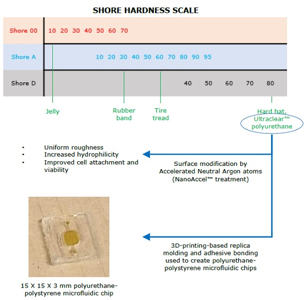
1. Introduction
2. Materials and Methods
2.1. General Recipe for PDMS, Blue Silicone R-2374 and PU
2.2. Optical Transmittance Studies
2.3. Feature Range Characterization
2.4. Scanning Electron Microscopy
2.5. Surface Modification by Corona Treatment
2.6. Surface Modification by NanoAccel™ Treatment in ANAB Mode
2.7. Water Contact Angle Measurement
2.8. Atomic Force Microscopy
2.9. Surface Energy Estimation
2.10. Fourier-Transform Infrared Spectroscopy in Attenuated Total Reflectance Mode
2.11. Cell Viability Studies
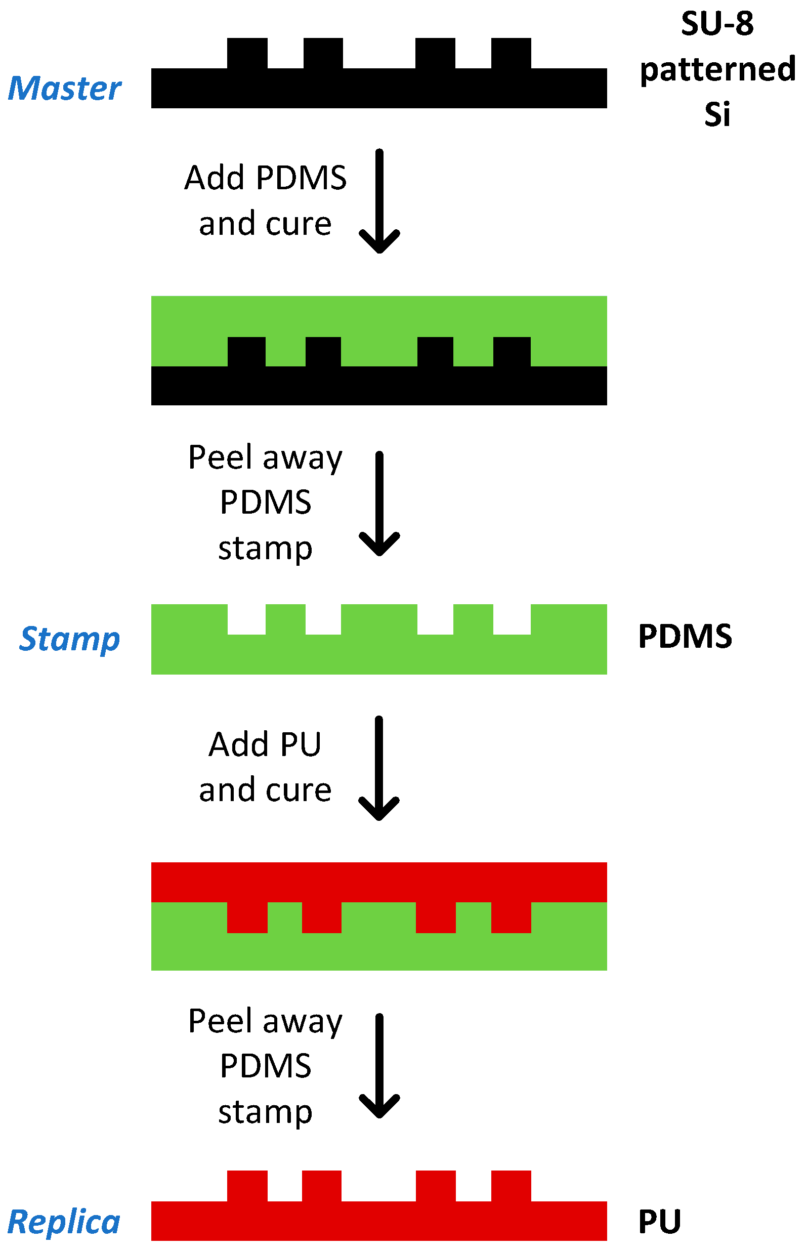
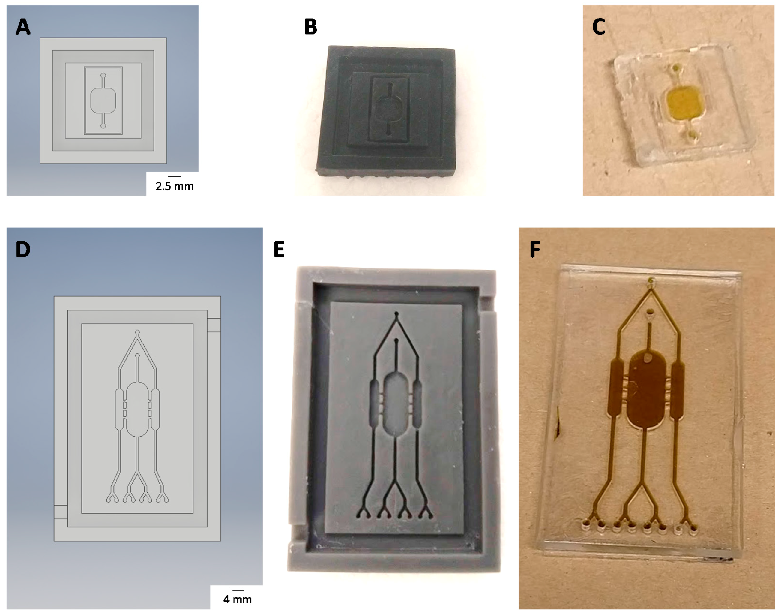
2.12. Chip Fabrication
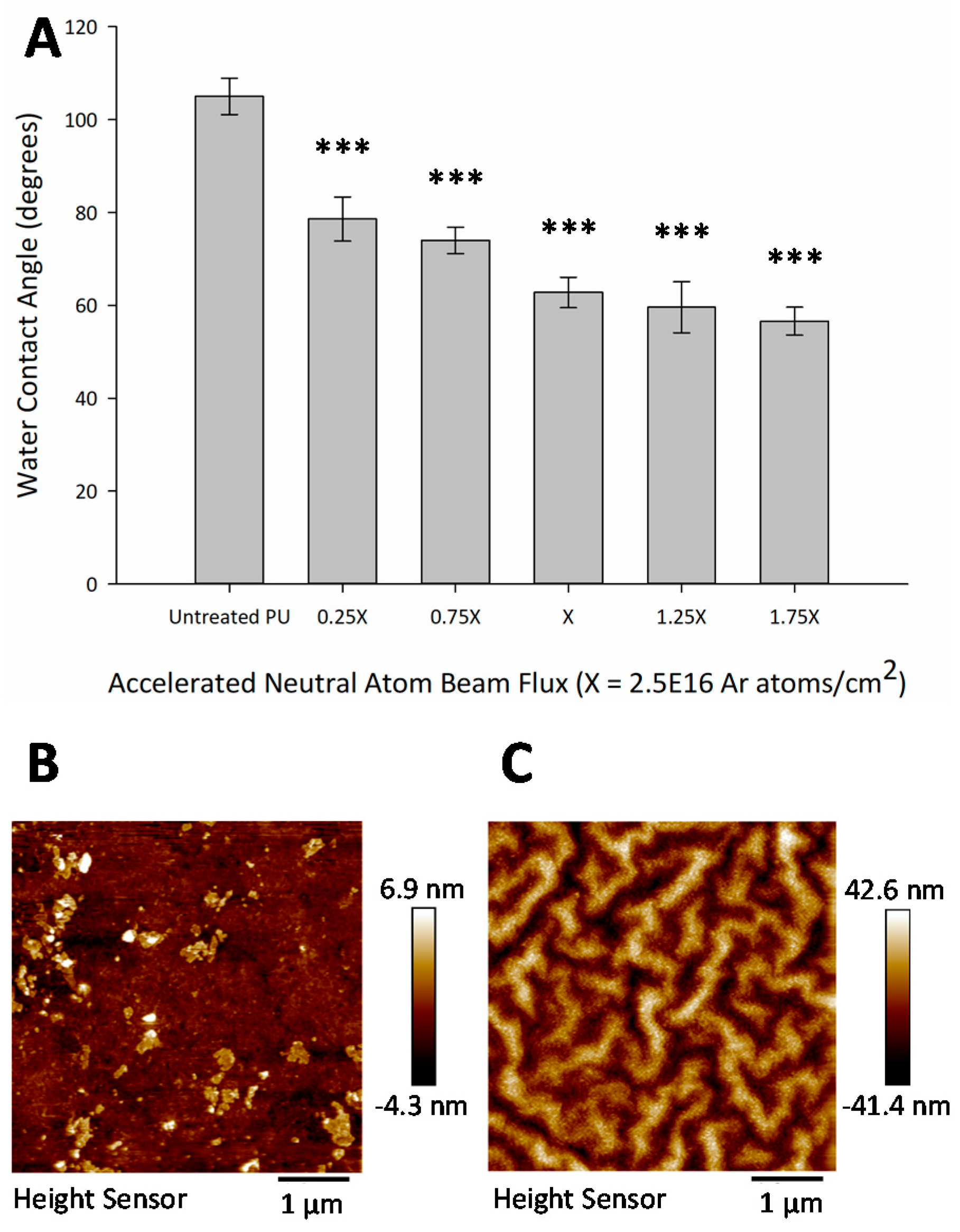
3. Results and Discussion
3.1. Optical Clarity
3.2. Microfluidic Range Achievable
3.3. Hydrophilic Surface Modification
3.4. Cell Viability
3.5. Chip Fabrication
4. Conclusions
Supplementary Materials
Author Contributions
Funding
Acknowledgments
Conflicts of Interest
References
- Sackmann, E.K.; Fulton, A.L.; Beebe, D.J. The present and future role of microfluidics in biomedical research. Nature 2014, 507, 181. [Google Scholar] [CrossRef] [PubMed]
- Reyes, D.R.; Iossifidis, D.; Auroux, P.-A.; Manz, A. Micro total analysis systems. 1. Introduction, theory, and technology. Anal. Chem. 2002, 74, 2623–2636. [Google Scholar] [CrossRef] [PubMed]
- El-Ali, J.; Sorger, P.K.; Jensen, K.F. Cells on chips. Nature 2006, 442, 403. [Google Scholar] [CrossRef] [PubMed]
- Hansen, C.; Quake, S.R. Microfluidics in structural biology: Smaller, faster em leader better. Curr. Opin. Struct. Biol. 2003, 13, 538–544. [Google Scholar] [CrossRef] [PubMed]
- Streets, A.M.; Huang, Y. Chip in a lab: Microfluidics for next generation life science research. Biomicrofluidics 2013, 7, 011302. [Google Scholar] [CrossRef] [PubMed]
- Domansky, K.; Leslie, D.C.; McKinney, J.; Fraser, J.P.; Sliz, J.D.; Hamkins-Indik, T.; Hamilton, G.A.; Bahinski, A.; Ingber, D.E. Clear castable polyurethane elastomer for fabrication of microfluidic devices. Lab Chip 2013, 13, 3956–3964. [Google Scholar] [CrossRef] [PubMed]
- Sia, S.K.; Whitesides, G.M. Microfluidic devices fabricated in poly(dimethylsiloxane) for biological studies. Electrophoresis 2003, 24, 3563–3576. [Google Scholar] [CrossRef]
- Sollier, E.; Murray, C.; Maoddi, P.; Di Carlo, D. Rapid prototyping polymers for microfluidic devices and high pressure injections. Lab Chip 2011, 11, 3752–3765. [Google Scholar] [CrossRef]
- Gervais, T.; El-Ali, J.; Gunther, A.; Jensen, K.F. Flow-induced deformation of shallow microfluidic channels. Lab Chip 2006, 6, 500–507. [Google Scholar] [CrossRef]
- Johnston, I.D.; Tracey, M.C.; Davis, J.B.; Tan, C.K.L. Micro throttle pump employing displacement amplification in an elastomeric substrate. J. Micromech. Microeng. 2005, 15, 1831. [Google Scholar] [CrossRef]
- Regehr, K.J.; Domenech, M.; Koepsel, J.T.; Carver, K.C.; Ellison-Zelski, S.J.; Murphy, W.L.; Schuler, L.A.; Alarid, E.T.; Beebe, D.J. Biological implications of polydimethylsiloxane-based microfluidic cell culture. Lab Chip 2009, 9, 2132–2139. [Google Scholar] [CrossRef] [PubMed]
- Eddington, D.T.; Puccinelli, J.P.; Beebe, D.J. Thermal aging and reduced hydrophobic recovery of polydimethylsiloxane. Sens. Actuators B Chem. 2006, 114, 170–172. [Google Scholar] [CrossRef]
- Kim, J.; Chaudhury, M.K.; Owen, M.J. Hydrophobic recovery of polydimethylsiloxane elastomer exposed to partial electrical discharge. J. Colloid Interface Sci. 2000, 226, 231–236. [Google Scholar] [CrossRef]
- Lee, J.N.; Park, C.; Whitesides, G.M. Solvent compatibility of poly(dimethylsiloxane)-based microfluidic devices. Anal. Chem. 2003, 75, 6544–6554. [Google Scholar] [CrossRef] [PubMed]
- Snyder, P.W.; Mecinović, J.; Moustakas, D.T.; Thomas, S.W.; Harder, M.; Mack, E.T.; Lockett, M.R.; Héroux, A.; Sherman, W.; Whitesides, G.M. Mechanism of the hydrophobic effect in the biomolecular recognition of arylsulfonamides by carbonic anhydrase. Proc. Natl. Acad. Sci. USA 2011, 108, 17889–17894. [Google Scholar] [CrossRef] [PubMed]
- Sarkar, A.; Kellogg, G.E. Hydrophobicity—Shake flasks, protein folding and drug discovery. Curr. Top. Med. Chem. 2010, 10, 67–83. [Google Scholar] [CrossRef] [PubMed]
- Devaraju, N.S.G.K.; Unger, M.A. Multilayer soft lithography of perfluoropolyether based elastomer for microfluidic device fabrication. Lab Chip 2011, 11, 1962–1967. [Google Scholar] [CrossRef]
- van Meer, B.J.; de Vries, H.; Firth, K.S.A.; van Weerd, J.; Tertoolen, L.G.J.; Karperien, H.B.J.; Jonkheijm, P.; Denning, C.; Ijzerman, A.P.; Mummery, C.L. Small molecule absorption by pdms in the context of drug response bioassays. Biochem. Biophys. Res. Commun. 2017, 482, 323–328. [Google Scholar] [CrossRef]
- Berthier, E.; Warrick, J.; Yu, H.; Beebe, D.J. Managing evaporation for more robust microscale assays part 1. Volume loss in high throughput assays. Lab Chip 2008, 8, 852–859. [Google Scholar] [CrossRef]
- Wu, M.H.; Dimopoulos, G.; Mantalaris, A.; Varley, J. The effect of hyperosmotic pressure on antibody production and gene expression in the gs-ns0 cell line. Biotechnol. Appl. Biochem. 2004, 40, 41–46. [Google Scholar]
- Dezengotita, V.M.; Kimura, R.; Miller, W.M. Effects of CO2 and osmolality on hybridoma cells: Growth, metabolism and monoclonal antibody production. Cytotechnology 1998, 28, 213–227. [Google Scholar] [CrossRef] [PubMed]
- Heo, Y.S.; Cabrera, L.M.; Song, J.W.; Futai, N.; Tung, Y.C.; Smith, G.D.; Takayama, S. Characterization and resolution of evaporation-mediated osmolality shifts that constrain microfluidic cell culture in poly(dimethylsiloxane) devices. Anal. Chem. 2007, 79, 1126–1134. [Google Scholar] [CrossRef] [PubMed]
- Mukhopadhyay, R. When pdms isn’t the best. Anal. Chem. 2007, 79, 3248–3253. [Google Scholar] [CrossRef] [PubMed]
- Becker, H.; Locascio, L.E. Polymer microfluidic devices. Talanta 2002, 56, 267–287. [Google Scholar] [CrossRef]
- Wu, W.I.; Sask, K.N.; Brash, J.L.; Selvaganapathy, P.R. Polyurethane-based microfluidic devices for blood contacting applications. Lab Chip 2012, 12, 960–970. [Google Scholar] [CrossRef] [PubMed]
- Piccin, E.; Coltro, W.K.; Fracassi da Silva, J.A.; Neto, S.C.; Mazo, L.H.; Carrilho, E. Polyurethane from biosource as a new material for fabrication of microfluidic devices by rapid prototyping. J. Chromatogr. A 2007, 1173, 151–158. [Google Scholar] [CrossRef] [PubMed]
- Alvankarian, J.; Majlis, B.Y. A new uv-curing elastomeric substrate for rapid prototyping of microfluidic devices. J. Micromech. Microeng. 2012, 22, 035006. [Google Scholar] [CrossRef]
- Stoyanov, I.; Tewes, M.; Koch, M.; Löhndorf, M. Microfluidic devices with integrated active valves based on thermoplastic elastomers. Microelectron. Eng. 2006, 83, 1681–1683. [Google Scholar] [CrossRef]
- Xu, Z.; Jiang, F.; Xu, Z.; Xu, H.; Ruan, X. Novel prototyping method for microfluidic devices based on thermoplastic polyurethane microcapillary film. Microfluid. Nanofluid. 2016, 20, 126. [Google Scholar] [CrossRef]
- Gu, P.; Nishida, T.; Fan, Z.H. The use of polyurethane as an elastomer in thermoplastic microfluidic devices and the study of its creep properties. Electrophoresis 2014, 35, 289–297. [Google Scholar] [CrossRef]
- Mehta, G.; Lee, J.; Cha, W.; Tung, Y.C.; Linderman, J.J.; Takayama, S. Hard top soft bottom microfluidic devices for cell culture and chemical analysis. Anal. Chem. 2009, 81, 3714–3722. [Google Scholar] [CrossRef]
- Xia, Y.; McClelland, J.J.; Gupta, R.; Qin, D.; Zhao, X.-M.; Sohn, L.L.; Celotta, R.J.; Whitesides, G.M. Replica molding using polymeric materials: A practical step toward nanomanufacturing. Adv. Mater. 1997, 9, 147–149. [Google Scholar] [CrossRef]
- Zhang, Y.; Lo, C.W.; Taylor, J.A.; Yang, S. Replica molding of high-aspect-ratio polymeric nanopillar arrays with high fidelity. Langmuir 2006, 22, 8595–8601. [Google Scholar] [CrossRef] [PubMed]
- Owens, C.E.; Hart, A.J. High-precision modular microfluidics by micromilling of interlocking injection-molded blocks. Lab Chip 2018, 18, 890–901. [Google Scholar] [CrossRef] [PubMed]
- Nargang, T.M.; Brockmann, L.; Nikolov, P.M.; Schild, D.; Helmer, D.; Keller, N.; Sachsenheimer, K.; Wilhelm, E.; Pires, L.; Dirschka, M.; et al. Liquid polystyrene: A room-temperature photocurable soft lithography compatible pour-and-cure-type polystyrene. Lab Chip 2014, 14, 2698–2708. [Google Scholar] [CrossRef] [PubMed]
- Khoury, J.; Kirkpatrick, S.R.; Maxwell, M.; Cherian, R.E.; Kirkpatrick, A.; Svrluga, R.C. Neutral atom beam technique enhances bioactivity of peek. Nuclear Instrum. Methods Phys. Res. Sect. B Beam Interact. Mater. Atoms 2013, 307, 630–634. [Google Scholar] [CrossRef]
- Kirkpatrick, A.; Kirkpatrick, S.; Walsh, M.; Chau, S.; Mack, M.; Harrison, S.; Svrluga, R.; Khoury, J. Investigation of accelerated neutral atom beams created from gas cluster ion beams. Nuclear Instrum. Methods Phys. Res. Sect. B Beam Interact. Mater. Atoms 2013, 307, 281–289. [Google Scholar] [CrossRef]
- Glick, C.C.; Srimongkol, M.T.; Schwartz, A.J.; Zhuang, W.S.; Lin, J.C.; Warren, R.H.; Tekell, D.R.; Satamalee, P.A.; Lin, L. Rapid assembly of multilayer microfluidic structures via 3d-printed transfer molding and bonding. Microsyst. Nanoeng. 2016, 2, 16063. [Google Scholar] [CrossRef]
- Au, A.K.; Huynh, W.; Horowitz, L.F.; Folch, A. 3d-printed microfluidics. Angew. Chem. 2016, 55, 3862–3881. [Google Scholar] [CrossRef]
- Zia, K.M.; Bhatti, I.A.; Barikani, M.; Zuber, M. Surface characteristics of uv-irradiated polyurethane elastomers extended with α, ω-alkane diols. Appl. Surf. Sci. 2008, 254, 6754–6761. [Google Scholar] [CrossRef]
- Souheng, W. Polymer Interface and Adhesion; Marcel Decker: New York, NY, USA, 1982. [Google Scholar]
- Rulison, C. So you want to measure surface energy. In A Tutorial Designed to Provide Basic Understanding of the Concept Solid Surface Energy, and Its Many Complications; TN306/CR; KRUSS GmbH: Hamburg, Germany, 1999; pp. 1–16. [Google Scholar]
- Kuang, P.; Constant, K.P. Increased Wettability and Surface Free Energy of Polyurethane by Ultraviolet Ozone Treatment; Materials Science and Engineering Publications, Iowa State University: Ames, IA, USA, 2015. [Google Scholar]
- Król, P.; Lechowicz, J.B.; Król, B. Modelling the surface free energy parameters of polyurethane coats—Part 1. Solvent-based coats obtained from linear polyurethane elastomers. Colloid Polym. Sci. 2013, 291, 1031–1047. [Google Scholar] [CrossRef] [PubMed]
- Wu, H.; Huang, B.; Zare, R.N. Construction of microfluidic chips using polydimethylsiloxane for adhesive bonding. Lab Chip 2005, 5, 1393–1398. [Google Scholar] [CrossRef] [PubMed]
- Satyanarayana, S.; Karnik, R.N.; Majumdar, A. Stamp-and-stick room-temperature bonding technique for microdevices. J. Microelectromech. Syst. 2005, 14, 392–399. [Google Scholar] [CrossRef]
- Dang, F.; Shinohara, S.; Tabata, O.; Yamaoka, Y.; Kurokawa, M.; Shinohara, Y.; Ishikawa, M.; Baba, Y. Replica multichannel polymer chips with a network of sacrificial channels sealed by adhesive printing method. Lab Chip 2005, 5, 472–478. [Google Scholar] [CrossRef] [PubMed]
- Rosu, D.; Rosu, L.; Cascaval, C.N. Ir-change and yellowing of polyurethane as a result of uv irradiation. Polym. Degrad. Stab. 2009, 94, 591–596. [Google Scholar] [CrossRef]
- Rabek, J.F. Polymer Photodegradation: Mechanisms and Experimental Methods; Springer Science & Business Media: Berlin, Germany, 2012. [Google Scholar]
- Planes, M.; Le Coz, C.; Soum, A.; Carlotti, S.; Rejsek-Riba, V.; Lewandowski, S.; Remaury, S.; Solé, S. Polydimethylsiloxane/additive systems for thermal and ultraviolet stability in geostationary environment. J. Spacecr. Rockets 2017, 53, 1128–1133. [Google Scholar] [CrossRef]
- Fischer, H.R.; Semprimoschnig, C.; Mooney, C.; Rohr, T.; van Eck, E.R.H.; Verkuijlen, M.H.W. Degradation mechanism of silicone glues under uv irradiation and options for designing materials with increased stability. Polym. Degrad. Stab. 2013, 98, 720–726. [Google Scholar] [CrossRef]
- Young, E.W.K.; Beebe, D.J. Fundamentals of microfluidic cell culture in controlled microenvironments. Chem. Soc. Rev. 2010, 39, 1036–1048. [Google Scholar] [CrossRef]
- Li, X.; Wu, N.; Rojanasakul, Y.; Liu, Y. Selective stamp bonding of pdms microfluidic devices to polymer substrates for biological applications. Sens. Actuators A Phys. 2013, 193, 186–192. [Google Scholar] [CrossRef]
- Dowling, D.P.; Miller, I.S.; Ardhaoui, M.; Gallagher, W.M. Effect of surface wettability and topography on the adhesion of osteosarcoma cells on plasma-modified polystyrene. J. Biomater. Appl. 2011, 26, 327–347. [Google Scholar] [CrossRef]
- Coates, J. Interpretation of infrared spectra, a practical approach. Encycl. Anal. Chem. 2000, 12, 10815–10837. [Google Scholar]
- Gaidukov, S.; Cabulis, U.; Gromilova, K.; Tupureina, V.; Grigalovica, A. Preparation and structural properties of free films from rapeseed oil-based rigid polyurethane-montmorillonite nanocomposites. Int. J. Polym. Sci. 2013, 2013. [Google Scholar] [CrossRef][Green Version]
- Badri, K.B.H.; Sien, W.C.; Shahrom, M.; Hao, L.C.; Baderuliksan, N.Y.; Norzali, N. Ftir spectroscopy analysis of the prepolymerization of palm-based polyurethane. J. Solid State Sci. Technol. 2010, 18, 1–8. [Google Scholar]
- Mi, S.; Du, Z.; Xu, Y.; Wu, Z.; Qian, X.; Zhang, M.; Sun, W. Microfluidic co-culture system for cancer migratory analysis and anti-metastatic drugs screening. Sci. Rep. 2016, 6, 35544. [Google Scholar] [CrossRef] [PubMed]
- TruongVo, T.N.; Kennedy, R.M.; Chen, H.; Chen, A.; Berndt, A.; Agarwal, M.; Zhu, L.; Nakshatri, H.; Wallace, J.; Na, S.; et al. Microfluidic channel for characterizing normal and breast cancer cells. J. Micromech. Microeng. 2017, 27, 035017. [Google Scholar] [CrossRef]
- Ren, X.; Ghassemi, P.; Babahosseini, H.; Strobl, J.S.; Agah, M. Single-cell mechanical characteristics analyzed by multiconstriction microfluidic channels. ACS Sens. 2017, 2, 290–299. [Google Scholar] [CrossRef]
- Karakas, H.E.; Kim, J.; Park, J.; Oh, J.M.; Choi, Y.; Gozuacik, D.; Cho, Y.-K. A microfluidic chip for screening individual cancer cells via eavesdropping on autophagy-inducing crosstalk in the stroma niche. Sci. Rep. 2017, 7, 2050. [Google Scholar] [CrossRef]
- Parizek, M.; Kasalkova, N.; Bacakova, L.; Slepicka, P.; Lisa, V.; Blazkova, M.; Svorcik, V. Improved adhesion, growth and maturation of vascular smooth muscle cells on polyethylene grafted with bioactive molecules and carbon particles. Int. J. Mol. Sci. 2009, 10, 4352–4374. [Google Scholar] [CrossRef]


| PU Treatment | Surface Energy (mN/m) | ||
|---|---|---|---|
| Polar | Dispersive | Total | |
| Untreated | 0.1 | 26.7 | 26.8 |
| 0.25X | 7.9 | 25.9 | 33.8 |
| 1X | 12.6 | 24.9 | 37.5 |
| 1.75X | 14.9 | 25.0 | 39.9 |
© 2019 by the authors. Licensee MDPI, Basel, Switzerland. This article is an open access article distributed under the terms and conditions of the Creative Commons Attribution (CC BY) license (http://creativecommons.org/licenses/by/4.0/).
Share and Cite
Dhall, A.; Masiello, T.; Gattu, S.; Strohmayer, M.; Butt, L.; Hemachandra, L.P.M.; Schujman, S.; Tokranova, N.; Khoury, J.; Papa Rao, S.; et al. Characterization and Neutral Atom Beam Surface Modification of a Clear Castable Polyurethane for Biomicrofluidic Applications. Surfaces 2019, 2, 100-116. https://doi.org/10.3390/surfaces2010009
Dhall A, Masiello T, Gattu S, Strohmayer M, Butt L, Hemachandra LPM, Schujman S, Tokranova N, Khoury J, Papa Rao S, et al. Characterization and Neutral Atom Beam Surface Modification of a Clear Castable Polyurethane for Biomicrofluidic Applications. Surfaces. 2019; 2(1):100-116. https://doi.org/10.3390/surfaces2010009
Chicago/Turabian StyleDhall, Atul, Tim Masiello, Suhasini Gattu, Matt Strohmayer, Logan Butt, Lewdeni Pathirannehelage Madhubhani Hemachandra, Sandra Schujman, Natalya Tokranova, Joseph Khoury, Satyavolu Papa Rao, and et al. 2019. "Characterization and Neutral Atom Beam Surface Modification of a Clear Castable Polyurethane for Biomicrofluidic Applications" Surfaces 2, no. 1: 100-116. https://doi.org/10.3390/surfaces2010009
APA StyleDhall, A., Masiello, T., Gattu, S., Strohmayer, M., Butt, L., Hemachandra, L. P. M., Schujman, S., Tokranova, N., Khoury, J., Papa Rao, S., Cady, N., Melendez, J. A., & Castracane, J. (2019). Characterization and Neutral Atom Beam Surface Modification of a Clear Castable Polyurethane for Biomicrofluidic Applications. Surfaces, 2(1), 100-116. https://doi.org/10.3390/surfaces2010009