Abstract
Electrodeposition of Pb on Au has been of interest for the variety of surface phenomena such as the UnderPotential Deposition (UPD) and surface alloying. Here, we examined the interface between the electrodeposited Pb film on Au, using surface sensitive techniques such as X-ray Photoelectron Spectroscopy (XPS), Ultraviolet Photoelectron Spectroscopy (UPS), Energy-Filtered Photoemission Electron Microscopy (EF-PEEM) and Work Function (WF) mapping. The initially electrodeposited Pb overlayer (~4 ML equivalent thickness) was transferred from the electrochemical cell to the UHV system. The deposited Pb layer was subjected to Argon sputtering cycles to remove oxide formed due to air exposure and gradually thinned down to a monolayer level. Surface science acquisitions showed the existence of a mixed oxide/metallic Pb overlayer at the monolayer level that transformed to a metallic Pb upon high temperature annealing (380 °C for 1 h) and measured changes of the electronic interaction that can be explained by Pb/Au surface alloy formation. The results show the electronic interaction between metallic Pb and Au is different from the interaction of Au with the PbO and Pb/PbO mixed layer; the oxide interface is less strained so the surface stress driven mixing between Au is not favored. The work illustrates applications of highly surface sensitive methods in the characterization of the surface alloy systems that can be extended to other complex and ultrathin mixed-metallic systems (designed or spontaneously formed).
1. Introduction
Electrodeposition of Pb on Au is a well-known system characterized by Stranski-Krastanov growth [1]. The electrodeposition of Pb on Au starts by the formation of the epitaxial monolayer positive from the equilibrium potential for bulk deposition known as Underpotential Deposition (UPD), followed by the nucleation of 3D islands in the OverPotential Deposition (OPD) region [2,3].
The UPD of Pb Monolayer (ML) on Au (111) has been considered as one of the model UPD systems and has been widely studied in the past few decades with a range of electrochemical and surface science techniques [2,4,5,6,7,8,9,10,11]. An incommensurate, electrocompressed closely packed hexagonal structure of a complete Pb UPD ML has been analyzed by a range of techniques including Scanning Tunneling Microscopy (STM), Atomic Force Microscopy (AFM), ex situ Low Energy Electron Diffraction (LEED) and in situ x-ray diffraction [8,12,13,14,15,16].
The UPD of Pb on Au has been used in a wide range of applications including measurements of surface area/roughness, surface structure characterization, chemical composition measurements, electrocatalysis, sensing as well as a mediation of the epitaxial thin film growth. For example, Pb UPD on Au has been used for the determination of surface areas, surface structures and crystallographic orientation of nanostructures such as gold nanorods [17], controlled-shape nanoparticles [17,18] and nanoporous gold electrodes [19]. The Au surfaces modified by a Pb UPD layer have shown to enhance the electrocatalytic activity and selectivity of oxygen reduction reactions [5,20,21], methanol oxidation [22] and glucose oxidation reactions [23,24]. Moreover, the Pb UPD layers have been successfully employed as mediators and manipulators of thin film growth kinetics in electrochemical methods such as the Surfactant-Mediated Growth (SMG) [25,26] and Defect Mediated Growth (DMG) [27,28] of epitaxial films of Ag, Co and Cu. In the recently developed Surface Limited Redox Replacement (SLRR) method, the UPD monolayer of Pb has been exploited as a sacrificial layer for the deposition of 2D epitaxial noble metal films, such as Pt, Ag, Au [26,29,30,31,32,33,34,35,36], nano-alloys [37,38,39,40] and nanoporous fuel-cell electrodes [41]. The SLRR method led to the development of a special class of highly active Pt-ML electrocatalysts for oxygen reduction reaction [42] and has become a tool for the design of model systems for fundamental electrocatalytic studies of structure-activity relationship [38] and catalytic stability [43]. The most recent advances include different ideas and concepts for a so-called electroless (e-less) deposition of Pb monolayer that were integrated into a deposition method called “electroless Atomic Layer Deposition” (e-less ALD) [44].
Pb on Au system is characterized by a large atomic size mismatch of 21%. Thus, it is an ideal model for studies of the surface-stress evolution and the related phenomena. This is an immiscible system, i.e., Pb and Au do not form bulk alloys. However, surface alloying has been reported in both electrochemical [6,7,45,46,47,48] and ultrahigh vacuum [49,50] environments. Several early studies argued that there was no evidence of surface alloy formation in this system [2,8,14,15]. However, later investigations, by in situ STM and surface stress measurements, showed the surface transformations that can be associated with the surface alloy formation/dissolution [6,7,46,47,48]. The in situ STM studies showed roughening of the initially flat Au substrate (by vacancy and ad-islands formation) after a Pb UPD layer dissolution [6,7,45,48]. The compressive stress evolution during monolayer formation of the magnitude of 1.2 N/m [48] featured a very narrow tensile drop within the main Pb UPD peak, corresponding to the formation of a high coverage Pb layer [47,48].
While most electrodeposition studies have been focused on Pb UPD, the bulk or so-called OPD for this system has not been studied so extensively [48]. The morphology of Pb OPD on Au studied by a combination of in situ STM [48] and ex situ AFM [3], have shown dependence on the deposition potential and specific ion adsorption (i.e. nature of ions in the deposition solution [3]). In the ionic liquid solution, the nucleation process of Pb leads to the formation of triangular-shaped vacancies on the Au (111), followed by the creation of large, well-defined 3D crystals of Pb [51]. The compressive stress evolution during 3D island creation as a result from isolated Pb island nucleation and growth has been studied in combination with the in situ Oblique-Incidence Reflectivity Difference (OIRD) [48]. The most intriguing was the observation of the surface alloy formation during OPD deposition that seems to be surface stress related and localized around the edge areas of 3D Pb crystals [48].
To better understand the phenomenon of surface alloy formation of Pb ML on Au, use of state-of-the-art characterization methods is required. In our work, we present results from X-ray Photoelectron Spectroscopy (XPS), Ultraviolet Photoelectron Spectroscopy (UPS), Energy-Filtered Photoemission Electron Microscopy (EF-PEEM) and Work Function (WF) mapping. XPS is a technique generally used to analyze the chemical composition of both bulk samples and surface alloys [52,53,54,55]. The UPS is a method that is highly surface sensitive and has been used to characterize a broad range of surface alloys, such as Au/Ni, Co/Cu(001) [52], Pt-bimetallic systems such as PtxM (M=Ni, Co, Fe, Ti, V) [53,56,57]. EF-PEEM and WF mapping are methods that can provide information about surface orientation and segregation [55,58,59]; also WF provides the information about surface activity [54]. These techniques are particularly useful due to their high surface sensitivity, ability to detect electronic changes from chemical environments at the Pb/Au interface and imaging capabilities at the nanoscale.
Studying Pb UPD on Au surface alloying is difficult as the UPD layer stability without the potential control can be compromised by exposure to air/oxygen [60]. Also, the bulk electrodeposited thicker Pb films inevitably oxidize in the air (i.e. forming of oxides). Therefore, the approach used in our work to study Pb ML level films was based on the deposition of bulk (OPD deposition) of equivalent 4 ML thickness films. Upon transfer from the electrochemical cell, PbO was removed gradually from the surface by cycles of Ar-sputtering and gentle annealing until the layer was thinned down to the desired ML level. Using a combination of XPS, UPS, EF-PEEM and WF mapping we then explored the structure of the layer.
2. Materials and Methods
Electrochemical measurements were performed in a standard three-electrode cell with a BioLogic VSP potentiostat (Bio-Logic Science Instruments SAS, Seyssinet-Pariset, France) and controlled by built-in software.
A solution containing 1 mM Pb(ClO4)2 and 100mM HClO4 was prepared by mixing high purity chemicals (PbCO3, 99.999%, Alfa Aesar, Heysham, UK and 70% HClO4, 99.999%, Sigma Aldrich, Steinheim, Germany). Before the experiment, the solution was deaerated with nitrogen gas (Oxygen Free Nitrogen, CAS: 7727-37-9, BOC, Manchester, UK) for 30 min. The oxygen free environment was maintained during the experiment with nitrogen flow above the solution.
Pb and Pt wires were used as pseudo Reference (RE) and Counter (CE) Electrodes respectively. Prior to experiments, the electrodes were prepared by cleaning in HNO3 (≥65%, Sigma Aldrich, Steinheim, Germany) for 10 s, rinsed with Milli-Q water (Millipore/Merck, Darmstadt, Germany) and dried with nitrogen. The Pt wire was then flame annealed by a butane torch. All the potentials will be reported with respect to the Pb pseudo RE (0.64 V vs Standard Hydrogen Electrode)
A vacuum evaporated Au thin film (250 nm) deposited on a glass slide (with a 4 nm Ti adhesion layer) was used as a Working Electrode (WE). Prior to experiments, the Au sample was cleaned with H2SO4 (95.0–97.0%, Sigma Aldrich, Steinheim, Germany) for 10 min, rinsed with Milli-Q water and dried with nitrogen. To obtain the Au (111) orientation, the sample was flame annealed for 2 min using a butane torch and rinsed with Milli-Q water.
The sample was then immersed in the deaerated solution with the half of its exposed surface area above the solution. The part of the substrate remained deposit-free, for the sake of comparison between the Pb covered and bare substrate. The deposition of Pb film was done by Linear Sweep Voltammetry (LSV) with a scan rate of 10 mV/s starting from the bare Au surface at a potential of 0.9 V to −0.1 V. The LSV potential range covered the Pb UPD ML deposition (between 0.9 V and 0.0 V) followed by the OPD growth (from 0.0V to −0.1 V). The potential of −0.1 V was then held constant for 20 s allowing for further (excess) overpotential Pb deposition. The sample was then removed from the cell, rinsed with Milli-Q water and dried with nitrogen gas. The equivalent thickness of the deposited Pb film of 4 ML was calculated by integration of the deposition current normalized by a charge of 305 μC/cm2 corresponding to an ‘ideal’ ML of Pb (111).
The prepared sample was immediately transferred into the Bristol NanoESCA Facility’s Ultra High Vacuum (UHV) chambers and heated overnight at 150 °C to clean the surface from physisorbed contaminants without desorbing and altering the deposited Pb. Other surface cleaning procedures involved 0.5 kV argon sputtering (at 45° to the sample normal) for 5 min and 2 min 30 s (for a total of 7 min 30 s), and a final 1 h anneal at 380 °C. All the surface analysis techniques were performed on both the Au and Pb deposited sides of the sample before proceeding to the next procedure. Throughout the experiments, the sample was kept in UHV chambers.
High resolution XPS was carried out using a monochromatic Al kα (hν = 1486.7 eV) excitation source, with the analyzer at 45° to the sample normal. A Pass Energy (PE) of 6 eV was used for detailed photoemission lines, giving an overall energy resolution of about 300 meV obtained by fitting the Fermi edge of the polycrystalline Au sample using a sigmoid function; PE of 50 eV was used for surveys. Angle resolved XPS acquisitions were performed using a non-monochromatic Al kα source and a PE of 50 eV.
The NanoESCA II EF-PEEM was used for WF mapping employing a non-monochromatic Hg source (hν ≈ 5.2 eV) with an overall energy resolution of about 140 meV and lateral resolution of about 150 nm. UPS was performed with monochromatic He-I (hν = 21.2 eV) and He-II (hν = 40.8 eV) with an overall energy resolution of about 140 meV. EF-PEEM was also used for chemical imaging on Pb 5d photoemission lines using a monochromated He-II (hν = 40.8 eV) source; a lateral resolution of about 500 nm and energy resolution of 0.9 eV was used to improve the signal-to-noise ratio.
3. Results
3.1. Core-Level Spectroscopy
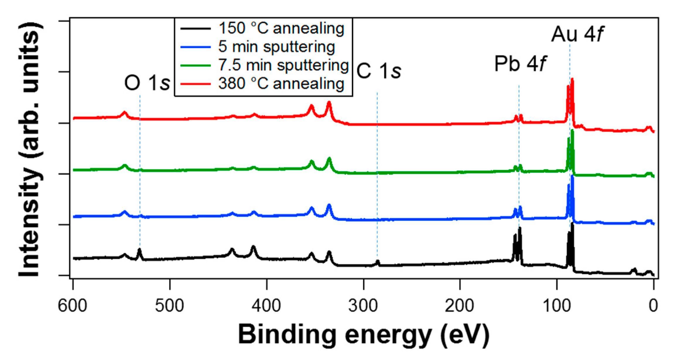
XPS is a surface sensitive technique that provides insight on the elemental composition and chemical environment of a sample. The presence of Pb on the Au surface was identified and quantified using XPS shown in Figure 1.
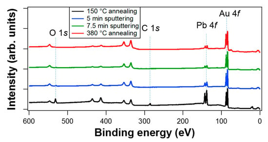
Figure 1.
XPS surveys of the Pb deposited on Au after 150 °C annealing (black), after 5 min of sputtering (blue), after 7 min 30 s of sputtering (green) and after 380 °C annealing (red). The spectra are shifted vertically for clarity.
XPS was carried out on the Pb deposited side of the sample after each heating and sputtering treatment stage, the XPS surveys are shown in Figure 1. After the first 150 °C annealing step, the XP spectrum showed the presence of Pb and Au, as well as carbon and oxygen from air contaminants and oxidation. 5 min sputtering was used to gently clean the surface [59,61], successfully removing the carbon contamination and significantly reducing the oxygen signal as well. However, the Pb quantity strongly decreased (see Table 1) and the remaining oxygen was predicted to be from oxidized Pb. Further argon sputtering for an extra 2 min 30 s did not appear to preferentially remove Pb oxide over metallic Pb, while annealing at 380 °C succeeded in removing the oxygen.

Table 1.
Tabulated key results obtained from XPS after each surface treatment step.
To investigate the presence of Pb oxide, detailed scans of the Pb 4f and O 1s photoemission lines were acquired, which are shown in Figure 2. After the initial 150 °C annealing step, the fitted Pb 4f peaks showed contributions from higher and lower binding energy (BE) doublets, which are from oxidized and metallic Pb, respectively. The higher BE of the oxide doublets was due to the higher electronegativity of oxygen with respect to Pb [62]. The O 1s peak also showed two components after the first annealing step, where the lower BE component was expected to be from Pb oxide, and the higher component to be mainly from oxygen on carbon contaminants [62,63]. This was further confirmed when 5 min of argon sputtering removed carbon, and significantly decreased the higher BE component of the O 1s peak.
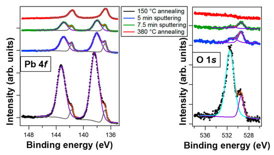
Figure 2.
Detailed XP spectra of the Pb 4f (left) and O 1s (right) emission lines of the Pb deposited on Au after different treatments, normalized by Au 4f areas. The acquired data are represented by the dotted lines while the peak deconvolutions are drawn as thin lines. The black, blue, green and red dotted lines represent the data after each treatment procedure, the same as in Figure 1. For Pb 4f the grey, purple and orange lines represent the fitted peaks for Pb metallic, Pb oxide and total fit respectively. For O 1s, the light blue, purple and orange lines represent the fitted peaks for oxygen bonded with carbon, with Pb and total fit respectively.
Table 1 lists the fitted BEs for the Pb-metal and Pb-oxide Pb 4f7/2 peaks, and the stoichiometry of Pb and O which were calculated by considering the Pb 4f area of oxidized Pb and the overall peak of O; the peak areas ratios were normalized by their sensitivity factors.
The stoichiometry of O and Pb were not reliable for the first measurement after the 150 °C annealing due to carbon and oxygen surface contamination. But after sputtering, the carbon contamination was removed and the O/Pb ratio after 5 and 7 min 30 s was found to be relatively constant at 0.9 and 0.8 respectively, indicating that the layer after sputtering was mainly composed of PbO. The BE of the Pb 4f7/2 oxide decreased significantly with the sputtering procedure from 138.3 eV to 138.0 eV, probably due to the formation of suboxides and damage to the surface due to Ar implantation (see also WF histograms discussion below).
Table 1 also reports the Pb overlayer estimated thicknesses. For the thickest layers of Pb (after 150 °C annealing and after 5 min sputtering), the coverages have been determined using angle resolved XPS as conducted in Ref. [64] approximating a homogeneous PbO layer. The coverage estimation by angle resolved acquisitions on much thinner layers (after 7 min 30 s of sputtering and 380 °C annealing) is not reliable due to the low signal of the overlayers and their complex morphology. Their coverages have therefore been extrapolated from the Au 4f/Pb 4f area ratio, calibrated with the overlayer thickness of the first two acquisitions. The monolayer coverages were obtained using the lattice parameter of PbO [65] after annealing at 150 °C, 5 and 7 min 30 s of sputtering and using the distance between atoms in bulk Pb (111) after the 380 °C anneal.
Comparing the ratio of Pb oxide to metallic in the Pb 4f photoemission lines after the 150 °C anneal, we observed a ratio of 12.0 which then dropped to 4.5 and 3.5 after the 5 min and 7 min 30 s of sputtering, respectively (see Table 1). The significant ratio difference after the first sputtering confirms that not all the Pb layer was homogenously oxidized. This was indirect evidence of Stranski- Krastanov growth, where the Pb islands, formed after the first monolayer, strongly oxidized when exposed to air due to their high surface areas and probably maintained only a very small core of metallic Pb. The first mild sputtering removed about half of the Pb layer (see Table 1), and the remaining layer was still partially oxidized but with the presence of more metallic Pb. Interestingly the oxide/metal ratio did not change drastically upon a further 2 min 30 s sputtering. This proves, along with a similar O/Pb stoichiometry, that the layer compositions at 1.8 ML and 1 ML of PbO are similar and that the oxides do not form a uniform passivating layer on the top of the Pb metal. On the contrary, the oxidation from air exposure created oxide particles all over the surface and therefore affected even the 1st Pb ML in contact with Au [16,66], see also EF-PEEM discussion below.
The final annealing was then performed at 380 °C to remove the Pb oxide without also desorbing the metal Pb [67]. From Figure 2, the Pb oxide and oxygen emission lines disappeared after the 380 °C anneal, but more interestingly, the metallic Pb peak increased significantly. This indicates that the annealing did not simply desorb Pb oxide from the Au surface, but rather removed some of the oxygen from the Pb oxide, probably facilitated by the Pb/Au interface. The calculated layer coverage after 7 min 30 s was estimated to be about 1 ML, this value is preserved after the 380 °C anneal (see Table 1), confirming the transformation of the mixed oxide-metal layer to an only metallic homogeneous overlayer. This latter finding is confirmed by WF maps, and EF-PEEM acquisition reported below.
3.2. Valence Band Photoemission and Photoemission Microscopy
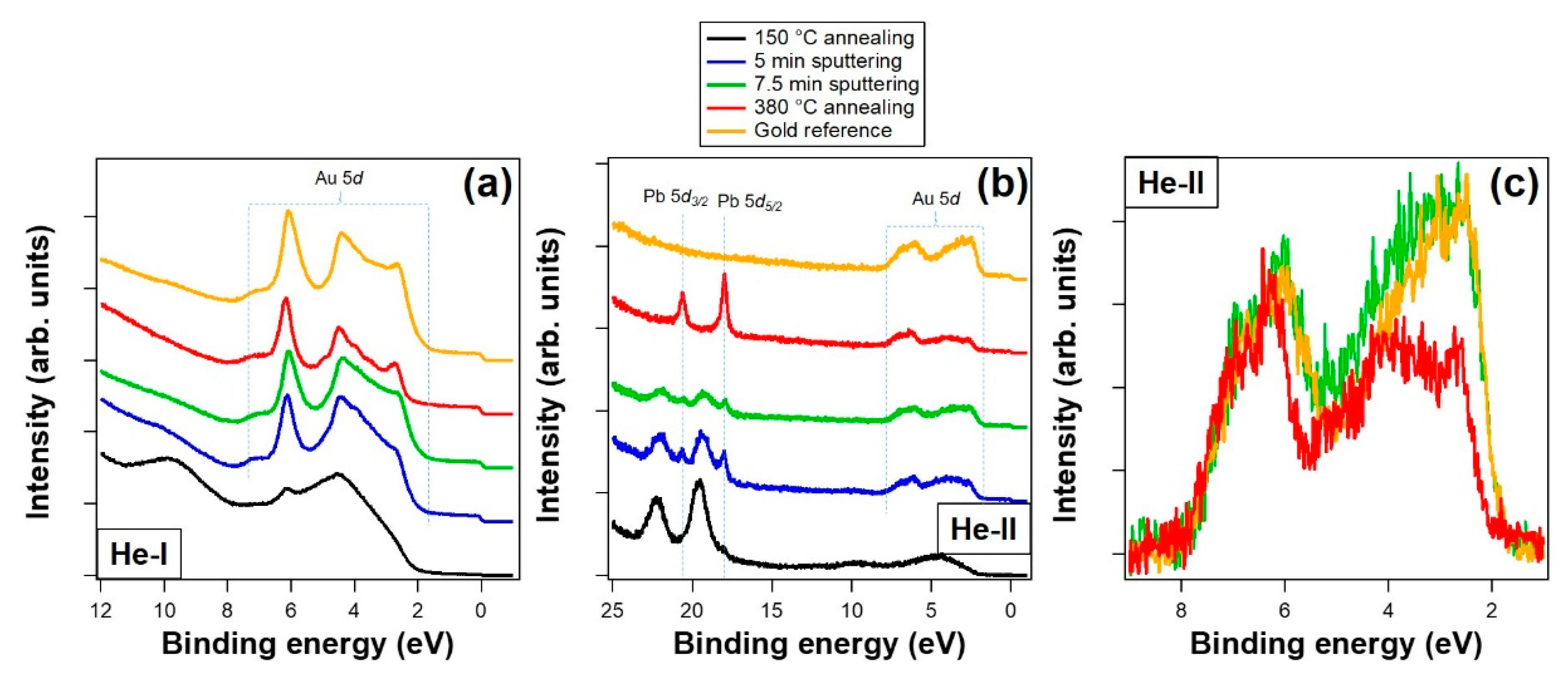
UPS (using He-I and He-II) was also performed on the sample after every annealing and sputtering procedure (Figure 3), allowing for a much higher surface sensitive characterization due to the lower photoelectron energies with respect to the XPS [68]. He-II (hν = 40.8 eV) is even more surface sensitive than He-I and allows for emission from the Pb 5d levels [69].
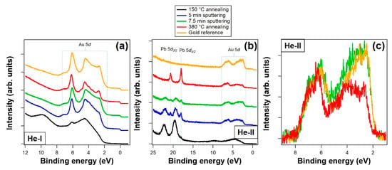
Figure 3.
UP spectra of Pb on Au after the different treatments, using (a) He-I and (b,c) He-II excitation. (c) shows a magnified, normalized and background subtracted region of the Au 5d bands after 7 min 30 s sputtering and annealing at 380 °C. UPS of the clean Au side of the sample is also plotted as a reference on all graphs. The spectra are indicated in black after 150 °C annealing, blue after 5 min of sputtering, green after 7 min 30 s of sputtering, red after 380 °C annealing and gold for the Au reference.
After the first annealing step (black lines), both UP spectra showed indistinct Au 5d bands, located between 2 and 7 eV [70,71], but showed two broad features at about at 4.5 and 9.8 eV, as seen in Figure 3a,b. Two distinct photoemission lines appeared at around 19.5 eV and 22.3 eV BE for the He-II spectrum of the sample. These correspond to the Pb 5d lines and have distinctly higher BEs than the 18.0 eV and 20.6 eV of metallic Pb [69] confirming the presence of Pb oxide in agreement with the XPS findings. The significantly higher oxide/metal ratio visible in Figure 3b with respect to the XPS was due to the much higher surface sensitivity of He-II UPS than XPS.
The 5 min of sputtering significantly sharpened the Au 5d band peaks in both the He-I and He-II UP spectra, while the Pb oxide peaks decreased and the metallic Pb peaks grew in intensity, indicating that metallic Pb was initially buried under the Pb oxide and carbon contamination. Further sputtering of 2 min 30 s reduced both the metallic and oxide peak areas. As found with XPS, the oxide/metal ratio visible in the Pb 5d region showed that between the 5 min and 7 min 30 s sputtering the layer compositions were very similar. Also, the presence of both oxide and metal on the surface after 7 min 30 s of sputtering showed the presence of oxide in contact with Au, further indicating that the metal in contact with Au oxidized during air exposure. Also confirmed by XPS, the final annealing at 380 °C completely removed the O from Pb and increased the metallic Pb signal at the oxide’s expense.
Figure 3c shows an enlarged view of the He-II UP spectra of the sample after the 7 min 30 s sputtering and 380 °C annealing along with undeposited Au region on the sample. The spectra were normalized to the Fermi edge and subtracted of a Shirley background for easier comparison. For the sample after 380 °C annealing, a clear shift in the Au 5d bands to higher BEs and shrinkage were observed, confirming electronic interactions between metallic Pb and Au. On the other hand, comparing the Au 5d bands after 7 min 30 s sputtering, the shift and shrinkage were minimal and possibly caused by the overlapping of the broad oxide features at 4.5 eV. Interestingly He-I acquisitions for the 380 °C annealed sample only showed a minimal shift in BE because the Au signal also originated from deeper atom layers, He-II was necessary for the extreme surface sensitivity sampling, almost exclusively at the Pb/Au interface.
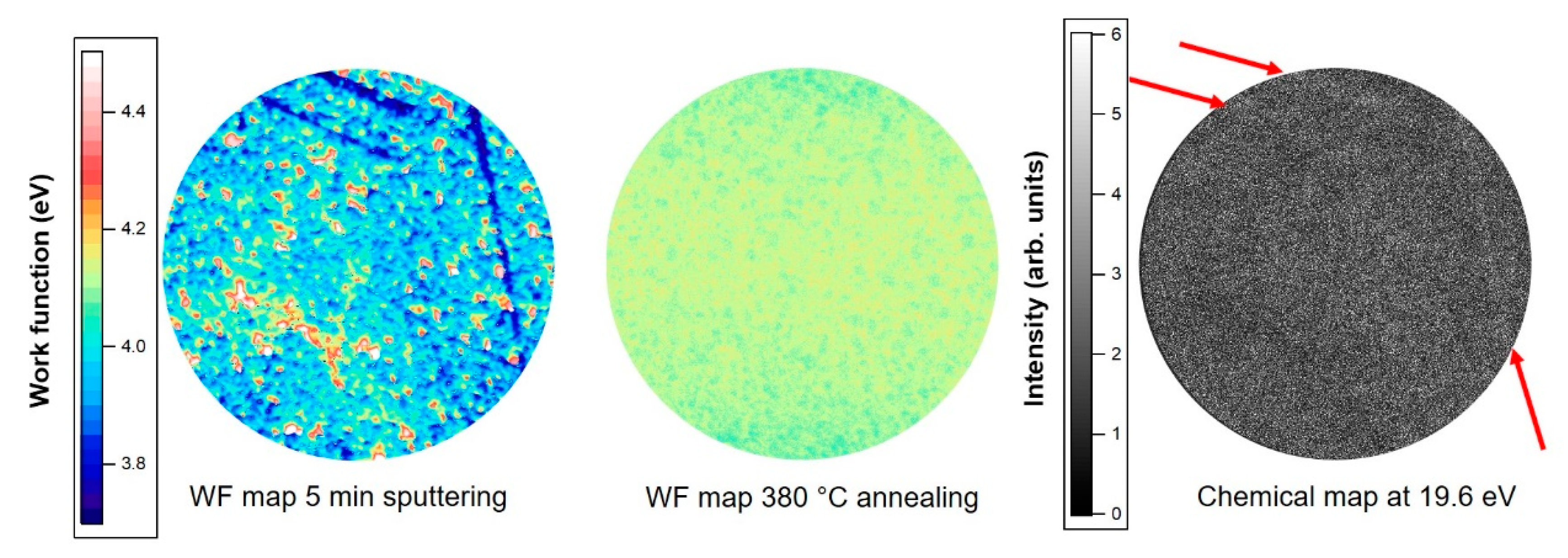
To visualize the surface structure at the nanoscale, the low energy emission cutoffs from EF-PEEM images were used to generate WF maps by performing an error function fitting at each pixel in the field of view. Figure 4 shows the WF maps of the same position of the sample after 5 min of sputtering, where the Pb signal was clear and without surface contamination, and after the final 380 °C annealing stage. The WF was roughly 3.95 eV and 4.15 eV respectively, in agreement with the literature where Pb oxide has a lower WF than metallic Pb [72,73], considering also that the high extractor voltage used in the PEEM reduces WF due to the Schottky effect [58].
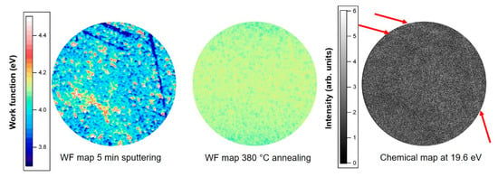
Figure 4.
WF maps of the Pb on Au after the 5 min sputtering (left) and 380 °C annealing (center) steps. On the (right), a normalized EF-PEEM image at 19.6 eV BE for Pb after 5 min of sputtering. The arrows are a guide to the eye highlighting some features in the image. The images were taken in the same area, with a field of view of 17.2 µm.
The WF map after 5 min sputtering showed a surface dominated by circular domains of about 300 nm in diameter, with a few stripes of low WF. EF-PEEM and WF maps obtained on the undeposited Au side (not reported here) also showed similar domains and stripes, indicating that they came from the substrate structure and that Pb OPD did not induce any changes in the general surface morphology as observed with the selected lateral resolution (150 nm).
EF-PEEM was performed using the He-II excitation on the Pb 5d5/2 emission line, providing a direct mapping of oxidized Pb at 19.6 eV. After 5 min sputtering, although very weak, some stripes of higher intensity can be seen on the chemical map (indicated by red arrows). These features are in the same position as the low WF stripes indicating that the low WF was due to Pb oxide. Notably, the chemical map shows also that the oxide was not only localized on the stripes, but it was distributed on all the sample’s surface. The poor lateral resolution (500 nm) and the low signal made it difficult to see its exact position, but it could be roughly related to the zone with WF < 4.1 eV in the WF map after 5 min of sputtering reported in Figure 4.
The WF contrast on the Pb side disappeared after annealing to 380 °C suggesting that the stripes were initially covered with Pb oxide but reduced to Pb after the annealing, confirming the transformation of part of the oxide into the metal as found in the XPS analysis. This finding is further confirmed by the fact that the chemical map at 18.0 eV (Pb 5d5/2 metallic) after annealing at 380 °C (not reported here) was homogeneous. Within our lateral resolution (150 nm), we could notice that the annealing process did not change the surface morphology.
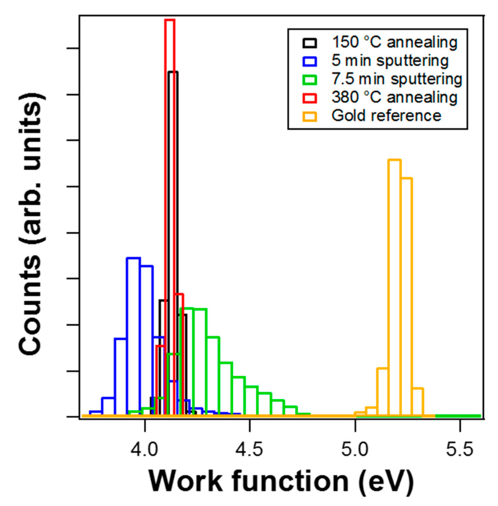
Histograms of all the WF maps were plotted in Figure 5 to show the distribution of WF across the surface after each treatment step.
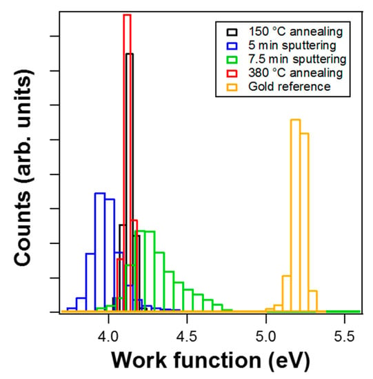
Figure 5.
WF distributions after each treatment step plotted as a histogram after 150 °C annealing (black), after 5 min of sputtering (blue), after 7 min 30 s of sputtering (green), after 380 °C annealing (red) and for the Au reference (golden). All the distributions were taken from the same area other than the Au reference, which was done on the undeposited half of the sample.
The WF varied throughout each step, where the sample at the first step (black) was carbon contaminated, then (blue) was cleaned, but further sputtering (green) increased the damage to the sample surface leading to surface roughening and broadening of the WF histogram; this broadening can also be related to the formation of suboxides as discussed above in the XPS section. With the final annealing (red), only metallic Pb remained on the surface with a very narrow WF distribution. The WF of the Pb film remained lower than WF of the polycrystalline Au [74] throughout each step, indicating that the OPD fully covered Au and the treatments did not expose the underlying Au, confirming the XPS coverage calculation in Table 1.
4. Discussion
With the combination of multiple surface sensitive techniques, we were able to determine the general structure of the Pb deposited on Au by OPD, its oxidation from exposure to atmosphere, the transformation of the surface with sputtering and annealing, and then the changes and shifts in the electronic bands from interaction between Au and Pb.
With XPS, we were able to determine the Pb oxidation species after sputtering to be PbO. The amount of deposited Pb was also quantified and found to be as expected from the OPD charge. Contaminants from the solution used in the electrochemical deposition were also not detected. XPS and UPS also gave an indirect insight into the nanostructure of the materials, confirming Stranski-Krastanov growth and that air oxidation reached the 1st Pb strained ML.
Moreover, we observed that the Pb layer thickness after 7 min 30 s sputtering and the 380 °C of annealing did not change. This might be an indication of type-I alloying, which agrees with the in situ STM results published by our group [48]. In type-I alloys, the surface adatoms are found to be diffusing on the surface and are highly mobile, due to the kinetics of alloying and repulsion [75]. Indeed, we have found that the Pb was able to migrate over to the clean Au side of the sample (over 2 mm migration) after annealing to 380 °C.
One particularly interesting finding is the interaction between Au and the metallic Pb from the UPS in Figure 3c (red curve). The shift to higher BE in the Au 5d bands could be a result of differential relaxation, exchange and correlation effects [76] due to the presence of Pb in the Au lattice [77]. Shifts in the 5d band have also been reported for Au alloys [70] and were explained by charge transfer and electron d-band repulsion where the band narrows [78]. Due to the alloying, the Au 5d peaks narrowed, and the spin-orbit splitting decreased and overall shifted to higher BEs, as observed with Au alloyed with Cd [77]. Comparing our findings to these reports we can assume we formed a Pb/Au surface alloy after the annealing at 380 °C.
From our UPS investigation we also showed that, in the case of partially oxidized Pb, the interaction with Au was negligible. The interfacial strain at the interface due to the Pb oxidation was lower than in the case of Pb metal. The Pb oxide affected the possibility of Pb metal to form a surface alloy surrounding it with oxide (see Figure 4) and eliminated the stress at the interface, which can explain why the Pb metal, present after only sputtering treatments, did not interact with Au. The high diffusion rate of Pb has been observed during annealing at high temperature. It is possible that the Pb-Au bond is much weaker at elevated temperatures compared to that at room temperature and the fast diffusion of Pb on the Au surface suggests almost ‘lattice gas’ behavior. In the presence of the metallic Pb, the system relaxes by minimizing the elastic energy through surface alloying. This is typical for immiscible and highly strained systems such as ours [79,80].
The high temperature annealing, removing the oxide and transforming it into metal, is the only treatment after which the metal enters in direct contact with the Au surface and forms a surface alloy. On the other hand, this treatment allows faster diffusion of Pb during which the alloy formation is not favorable. In future papers, we will explore these and similar materials at different temperatures to investigate the interplay between the surface alloying and surface interaction (ad-atom diffusion).
Author Contributions
Data curation, M.C.; Funding acquisition, N.A.F.; Investigation, A.S., G.W. and M.C.; Methodology, A.S., N.V., G.W. and M.C.; Supervision, M.C., N.A.F. and N.V.; Validation, M.C. and N.V.; Visualization, M.C.; Writing—original draft, A.S., G.W. and M.C.; Writing—review & editing, A.S., M.C., N.A.F. and N.V.
Funding
This research was partially funded by EPSRC Strategic Equipment, Grant number EP/K035746/1 and EP/M000605/1; Ph.D. studentships are funded through BCFN: EPSRC (EP/L016648/1), and Renewtec Technologies, Al Hamad Group.
Acknowledgments
The authors acknowledge the Bristol NanoESCA Facility (EPSRC Strategic Equipment Grant EP/K035746/1 and EP/M000605/1). A.S. and G.W. acknowledge Ph.D. studentships funded through BCFN: EPSRC (EP/L016648/1), and Renewtec Technologies, Al Hamad Group, respectively.
Conflicts of Interest
The authors declare no conflict of interest.
References
- Obretenov, W.; Schmidt, U.; Lorenz, W.J.; Staikov, G.; Budevski, E.; Carnal, D.; Müller, U.; Siegenthaler, H.; Schmidt, E. Underpotential Deposition and Electrocrystallization of Metals An Atomic View by Scanning Tunneling Microscopy. J. Electrochem. Soc. 1993, 140, 692–703. [Google Scholar] [CrossRef]
- Hamelin, A.; Lipkowski, J. Underpotential deposition of lead on gold single crystal faces: Part II. General discussion. J. Electroanal. Chem. Interfacial Electrochem. 1984, 171, 317–330. [Google Scholar] [CrossRef]
- Wu, G.Y.; Schwarzacher, W. The effect of halide additives on the electrodeposition of Pb on polycrystalline Au. J. Electroanal. Chem. 2009, 629, 164–168. [Google Scholar] [CrossRef]
- Adzic, R.; Yeager, E.; Cahan, B. Optical and Electrochemical Studies of Underpotential Deposition of Lead on Gold Evaporated and Single-Crystal Electrodes. J. Electrochem. Soc. 1974, 121, 474–484. [Google Scholar] [CrossRef]
- Alvarez-Rizatti, M.; Jüttner, K. Electrocatalysis of oxygen reduction by UPD of lead on gold single-crystal surfaces. J. Electroanal. Chem. Interfacial Electrochem. 1983, 144, 351–363. [Google Scholar] [CrossRef]
- Green, M.P.; Hanson, K.J.; Carr, R.; Lindau, I. STM Observations of the Underpotential Deposition and Stripping of Pb on Au(111) under Potential Sweep Conditions. J. Electrochem. Soc. 1990, 137, 3493–3498. [Google Scholar] [CrossRef]
- Green, M.P.; Hanson, K.J. Alloy formation in an electrodeposited monolayer. Surf. Sci. 1991, 259, L743–L749. [Google Scholar] [CrossRef]
- Toney, M.F.; Gordon, J.G.; Samant, M.G.; Borges, G.L.; Melroy, O.R. In-Situ Atomic Structure of Underpotentially Deposited Monolayers of Pb and Tl on Au(111) and Ag(111): A Surface X-ray Scattering Study. J. Phys. Chem. 1995, 99, 4733–4744. [Google Scholar] [CrossRef]
- Lorenz, W.J.; Staikov, G. 2D and 3D thin film formation and growth mechanisms in metal electrocrystallization—An atomistic view by in situ STM. Surf. Sci. 1995, 335, 32–43. [Google Scholar] [CrossRef]
- Herrero, E.; Buller, L.J.; Abruña, H.D. Underpotential Deposition at Single Crystal Surfaces of Au, Pt, Ag and Other Materials. Chem. Rev. 2001, 101, 1897–1930. [Google Scholar] [CrossRef]
- Hsieh, S.-J.; Gewirth, A.A. Poisoning the catalytic reduction of peroxide on Pb underpotential deposition modified Au surfaces with iodine. Surf. Sci. 2002, 498, 147–160. [Google Scholar] [CrossRef]
- Ganon, J.P.; Clavilier, J. Electrochemical adsorption of lead and bismuth at gold single crystal surfaces with vicinal (111) orientations. I. Surf. Sci. 1984, 145, 487–518. [Google Scholar] [CrossRef]
- Samant, M.G.; Toney, M.F.; Borges, G.L.; Blum, L.; Melroy, O.R. Grazing incidence x-ray diffraction of lead monolayers at a silver (111) and gold (111) electrode/electrolyte interface. J. Phys. Chem. 1988, 92, 220–225. [Google Scholar] [CrossRef]
- Tao, N.J.; Pan, J.; Li, Y.; Oden, P.I.; DeRose, J.A.; Lindsay, S.M. Initial stage of underpotential deposition of Pb on reconstructed and unreconstructed Au(111). Surf. Sci. 1992, 271, L338–L344. [Google Scholar] [CrossRef]
- Chen, C.H.; Washburn, N.; Gewirth, A.A. In situ atomic force microscope study of lead underpotential deposition on gold (111): Structural properties of the catalytically active phase. J. Phys. Chem. 1993, 97, 9754–9760. [Google Scholar] [CrossRef]
- Crepaldi, A.; Pons, S.; Frantzeskakis, E.; Calleja, F.; Etzkorn, M.; Seitsonen, A.P.; Kern, K.; Brune, H.; Grioni, M. Combined ARPES and STM study of Pb/Au(111) Moiré structure: One overlayer, two symmetries. Phys. Rev. B 2013, 87. [Google Scholar] [CrossRef]
- Hernández, J.; Solla-Gullón, J.; Herrero, E.; Aldaz, A.; Feliu, J.M. Characterization of the Surface Structure of Gold Nanoparticles and Nanorods Using Structure Sensitive Reactions. J. Phys. Chem. B 2005, 109, 12651–12654. [Google Scholar] [CrossRef]
- Jeyabharathi, C.; Zander, M.; Scholz, F. Underpotential deposition of lead on quasi-spherical and faceted gold nanoparticles. J. Electroanal. Chem. 2017. [Google Scholar] [CrossRef]
- Liu, Y.; Bliznakov, S.; Dimitrov, N. Comprehensive Study of the Application of a Pb Underpotential Deposition-Assisted Method for Surface Area Measurement of Metallic Nanoporous Materials. J. Phys. Chem. C 2009, 113, 12362–12372. [Google Scholar] [CrossRef]
- Adžić, R.R.; Tripkovic, A.V.; Markovic, N.M. Oxygen reduction on electrode surfaces modified by foreign metal ad-atoms: Lead ad-atoms on gold. J. Electroanal. Chem. 1980, 114, 37–51. [Google Scholar] [CrossRef]
- Wang, Y.; Laborda, E.; Plowman, B.J.; Tschulik, K.; Ward, K.R.; Palgrave, R.G.; Damm, C.; Compton, R.G. The strong catalytic effect of Pb(II) on the oxygen reduction reaction on 5 nm gold nanoparticles. Phys. Chem. Chem. Phys. 2014, 16, 3200–3208. [Google Scholar] [CrossRef] [PubMed]
- Hernández, J.; Solla-Gullón, J.; Herrero, E.; Aldaz, A.; Feliu, J.M. Methanol oxidation on gold nanoparticles in alkaline media: Unusual electrocatalytic activity. Electrochim. Acta 2006, 52, 1662–1669. [Google Scholar] [CrossRef]
- Chen, Y.; Milenkovic, S.; Hassel, A.W. {110}-Terminated Square-Shaped Gold Nanoplates and Their Electrochemical Surface Reactivity. ChemElectroChem 2017, 4, 557–564. [Google Scholar] [CrossRef]
- Yu, L.; Akolkar, R. Lead underpotential deposition for the surface characterization of silver ad-atom modified gold electrocatalysts for glucose oxidation. J. Electroanal. Chem. 2017, 792, 61–65. [Google Scholar] [CrossRef]
- Brankovic, S.R.; Dimitrov, N.; Sieradzki, K. Surfactant Mediated Electrochemical Deposition of Ag on Au(111). Electrochem. Solid State Lett. 1999, 2, 443–445. [Google Scholar] [CrossRef]
- Wu, D.; Solanki, D.J.; Joi, A.; Dordi, Y.; Dole, N.; Litvnov, D.; Brankovic, S.R. Pb Monolayer Mediated Thin Film Growth of Cu and Co: Exploring Different Concepts. J. Electrochem. Soc. 2019, 1666, D3013–D3021. [Google Scholar] [CrossRef]
- Sieradzki, K.; Dimitrov, N. Electrochemical Defect-Mediated Thin-Film Growth. Science 1999, 284, 138. [Google Scholar] [CrossRef]
- Hwang, S.; Oh, I.; Kwak, J. Electrodeposition of Epitaxial Cu(111) Thin Films on Au(111) Using Defect-Mediated Growth. J. Am. Chem. Soc. 2001, 123, 7176–7177. [Google Scholar] [CrossRef]
- Viyannalage, L.T.; Vasilic, R.; Dimitrov, N. Epitaxial Growth of Cu on Au(111) and Ag(111) by Surface Limited Redox ReplacementAn Electrochemical and STM Study. J. Phys. Chem. C 2007, 111, 4036–4041. [Google Scholar] [CrossRef]
- Fayette, M.; Liu, Y.; Bertrand, D.; Nutariya, J.; Vasiljevic, N.; Dimitrov, N. From Au to Pt via Surface Limited Redox Replacement of Pb UPD in One-Cell Configuration. Langmuir 2011, 27, 5650–5658. [Google Scholar] [CrossRef]
- Jayaraju, N.; Viravapandian, D.; Kim, G.Y.; Banga, D.; Stickney, J.L. Electrochemical Atomic Layer Deposition (E-ALD) of Pt Nanofilms Using SLRR Cycles. J. Electrochem. Soc. 2012, 159, D616–D622. [Google Scholar] [CrossRef]
- Ambrozik, S.; Rawlings, B.; Vasiljevic, N.; Dimitrov, N. Metal deposition via electroless surface limited redox replacement. Electrochem. Commun. 2014, 44, 19–22. [Google Scholar] [CrossRef]
- Dimitrov, N. Recent Advances in the Growth of Metals, Alloys, and Multilayers by Surface Limited Redox Replacement (SLRR) Based Approaches. Electrochim. Acta 2016, 209, 599–622. [Google Scholar] [CrossRef]
- Al Amri, Z.; Mercer, M.P.; Vasiljevic, N. Surface Limited Redox Replacement Deposition of Platinum Ultrathin Films on Gold: Thickness and Structure Dependent Activity towards the Carbon Monoxide and Formic Acid Oxidation reactions. Electrochim. Acta 2016, 210, 520–529. [Google Scholar] [CrossRef]
- Brankovic, S.R. Fundamentals of Metal Deposition via Surface Limited Redox Replacement of Underpotentially-Deposited Monolayer. Electrochem. Soc. Interface 2018, 27, 57–63. [Google Scholar] [CrossRef]
- Brankovic, S.R.; Wang, J.X.; Adžić, R.R. Metal monolayer deposition by replacement of metal adlayers on electrode surfaces. Surf. Sci. 2001, 474, L173–L179. [Google Scholar] [CrossRef]
- Mercer, M.P.; Plana, D.; Fermiotan, D.J.; Morgan, D.; Vasiljevic, N. Growth of epitaxial Pt1-xPbx alloys by surface limited redox replacement and study of their adsorption properties. Langmuir 2015, 31, 10904–10912. [Google Scholar] [CrossRef]
- Vasiljevic, N. Electrodeposition of Pt-bimetallic Model Systems for Electrocatalysis and Electrochemical Surface Science. Electrochem. Soc. Interface 2018, 27, 71–75. [Google Scholar] [CrossRef]
- Zhang, J.; Vukmirovic, M.B.; Sasaki, K.; Nilekar, A.U.; Mavrikakis, M.; Adzic, R.R. Mixed-Metal Pt Monolayer Electrocatalysts for Enhanced Oxygen Reduction Kinetics. J. Am. Chem Soc. 2005, 127, 12480–12481. [Google Scholar] [CrossRef]
- Bromberg, L.; Fayette, M.; Martens, B.; Luo, Z.P.; Wang, Y.; Xu, D.; Zhang, J.; Fang, J.; Dimitrov, N. Catalytic Performance Comparison of Shape-Dependent Nanocrystals and Oriented Ultrathin Films of Pt4Cu Alloy in the Formic Acid Oxidation Process. Electrocatalysis 2012, 1–13. [Google Scholar] [CrossRef]
- McCurry, D.; Kamundi, M.; Fayette, M.; Wafula, F.; Dimitrov, N. All Electrochemical Fabrication of a Platinized Nanoporous Au Thin-Film Catalyst. ACS Appl. Mater. Interfaces 2011, 3, 4459–4468. [Google Scholar] [CrossRef] [PubMed]
- Adzic, R.R.; Zhang, J.; Sasaki, K.; Vukmirovic, M.B.; Shao, M.; Wang, J.X.; Nilekar, A.U.; Mavrikakis, M.; Valerio, J.A.; Uribe, F. Platinum Monolayer Fuel Cell Electrocatalysts. Top. Catal. 2007, 46, 249–262. [Google Scholar] [CrossRef]
- Fayette, M.; Nutariya, J.; Vasiljevic, N.; Dimitrov, N. A Study of Pt Dissolution during Formic Acid Oxidation. ACS Catalysis 2013, 3, 1709–1718. [Google Scholar] [CrossRef]
- Wu, D.; Solanki, D.J.; Ramirez, J.L.; Yang, W.; Joi, A.; Dordi, Y.; Dole, N.; Brankovic, S.R. Electroless Deposition of Pb Monolayer: A New Process and Application to Surface Selective Atomic Layer Deposition. Langmuir 2018, 34, 11384–11394. [Google Scholar] [CrossRef] [PubMed]
- Green, M.; Hanson, K.; Scherson, D.; Xing, X.; Richter, M.; Ross, P.; Carr, R.; Lindau, I. In situ scanning tunneling microscopy studies of the underpotential deposition of lead on gold (111). J. Phys. Chem. 1989, 93, 2181–2184. [Google Scholar] [CrossRef]
- Stafford, G.R.; Bertocci, U. In Situ Stress and Nanogravimetric Measurements During Underpotential Deposition of Pb on (111)-Textured Au. J. Phys. Chem. C 2007, 111, 17580–17586. [Google Scholar] [CrossRef]
- Shin, J.W.; Bertocci, U.; Stafford, G.R. Stress Response to Surface Alloying and Dealloying during Underpotential Deposition of Pb on (111)-Textured Au. J. Phys. Chem. C 2010, 114, 7926–7932. [Google Scholar] [CrossRef]
- Nutariya, J.; Velleuer, J.; Schwarzacher, W.; Vasiljevic, N. Surface alloying/dealloying in Pb/Au (111) system. ECS Trans. 2010, 28, 15–25. [Google Scholar] [CrossRef]
- Biberian, J.P.; Rhead, G.E. Spontaneous alloying of a gold substrate with lead monolayers. J. Phys. F Met. Phys. 1973, 3, 675–682. [Google Scholar] [CrossRef]
- Perdereau, J.; Biberian, J.P.; Rhead, G.E. Adsorption and surface alloying of lead monolayers on (111) and (110) faces of gold. J. Phys. F Met. Phys. 1974, 4, 798. [Google Scholar] [CrossRef]
- Wang, F.-X.; Pan, G.-B.; Liu, Y.-D.; Xiao, Y. Pb deposition onto Au(111) from acidic chloroaluminate ionic liquid. Chem. Phys. Lett. 2010, 488, 112–115. [Google Scholar] [CrossRef]
- Kim, S.K.; Kim, J.S.; Han, J.Y.; Seo, J.M.; Lee, C.K.; Hong, S.C. Surface alloying of a Co film on the Cu(001) surface. Surf. Sci. 2000, 453, 47–58. [Google Scholar] [CrossRef]
- Stamenkovic, V.R.; Mun, B.S.; Mayrhofer, K.J.J.; Ross, P.N.; Markovic, N.M. Effect of Surface Composition on Electronic Structure, Stability, and Electrocatalytic Properties of Pt-Transition Metal Alloys: Pt-Skin versus Pt-Skeleton Surfaces. J. Am. Chem. Soc. 2006, 128, 8813–8819. [Google Scholar] [CrossRef] [PubMed]
- Tang, Q.; Zhang, H.; Meng, Y.; He, B.; Yu, L. Dissolution Engineering of Platinum Alloy Counter Electrodes in Dye-Sensitized Solar Cells. Angew. Chem. Int. Ed. 2015, 54, 11448–11452. [Google Scholar] [CrossRef] [PubMed]
- Ali-Löytty, H.; Hannula, M.; Honkanen, M.; Östman, K.; Lahtonen, K.; Valden, M. Grain orientation dependent Nb–Ti microalloying mediated surface segregation on ferritic stainless steel. Corros. Sci. 2016, 112, 204–213. [Google Scholar] [CrossRef]
- Stamenkovic, V.R.; Mun, B.S.; Arenz, M.; Mayrhofer, K.J.J.; Lucas, C.A.; Wang, G.; Ross, P.N.; Markovic, N.M. Trends in electrocatalysis on extended and nanoscale Pt-bimetallic alloy surfaces. Nat. Mater. 2007, 6, 241. [Google Scholar] [CrossRef] [PubMed]
- Mun, B.S.; Watanabe, M.; Rossi, M.; Stamenkovic, V.R.; Markovic, N.M.; Ross, P.N. A study of electronic structures of Pt3M (M=Ti,V,Cr,Fe,Co,Ni) polycrystalline alloys with valence-band photoemission spectroscopy. J. Chem. Phys. 2005, 123, 204717. [Google Scholar] [CrossRef]
- Renault, O.; Brochier, R.; Roule, A.; Haumesser, P.H.; Krömker, B.; Funnemann, D. Work-function imaging of oriented copper grains by photoemission. Surf. Interface Anal. 2006, 38, 375–377. [Google Scholar] [CrossRef]
- Tiwari, D.; Cattelan, M.; Harniman, R.L.; Sarua, A.; Abbas, A.; Bowers, J.W.; Fox, N.A.; Fermin, D.J. Mapping Shunting Paths at the Surface of Cu2ZnSn(S,Se)4 Films via Energy-Filtered Photoemission Microscopy. iScience 2018, 9, 36–46. [Google Scholar] [CrossRef]
- Vasilic, R.; Vasiljevic, N.; Dimitrov, N. Open Circuit Stability of Underpotentially Deposited Pb Monolayer on Cu(111). J. Elecatroanal. Chem. 2005, 580, 203–212. [Google Scholar] [CrossRef]
- Tiwari, D.; Cattelan, M.; Harniman, R.L.; Sarua, A.; Fox, N.; Koehler, T.; Klenk, R.; Fermin, D.J. Impact of Sb and Na Doping on the Surface Electronic Landscape of Cu2ZnSnS4 Thin Films. ACS Energy Lett. 2018, 2977–2982. [Google Scholar] [CrossRef]
- Kim, K.S.; O’Leary, T.J.; Winograd, N. X-ray photoelectron spectra of lead oxides. Anal. Chem. 1973, 45, 2214–2218. [Google Scholar] [CrossRef]
- Desimoni, E.; Casella, G.I.; Morone, A.; Salvi, A.M. XPS determination of oxygen-containing functional groups on carbon-fibre surfaces and the cleaning of these surfaces. Surf. Interface Anal. 1990, 15, 627–634. [Google Scholar] [CrossRef]
- Fadley, C.S. Angle-resolved x-ray photoelectron spectroscopy. Prog. Surf. Sci. 1984, 16, 275–388. [Google Scholar] [CrossRef]
- Light, T.B.; Eldridge, J.M.; Matthews, J.W.; Greiner, J.H. Structure of thin lead oxide layers as determined by x−ray diffraction. J. Appl. Phys. 1975, 46, 1489–1492. [Google Scholar] [CrossRef]
- Brunt, T.A.; Rayment, T.; O’Shea, S.J.; Welland, M.E. Measuring the Surface Stresses in an Electrochemically Deposited Metal Monolayer: Pb on Au(111). Langmuir 1996, 12, 5942–5946. [Google Scholar] [CrossRef]
- Vurens, G.H.; Salmeron, M.; Somorjai, G.A. The preparation of thin ordered transition metal oxide films on metal single crystals for surface science studies. Prog. Surf. Sci. 1989, 32, 333–360. [Google Scholar] [CrossRef]
- Seah, M.P.; Dench, W.A. Quantitative electron spectroscopy of surfaces: A standard data base for electron inelastic mean free paths in solids. Surf. Interface Anal. 1979, 1, 2–11. [Google Scholar] [CrossRef]
- Nyholm, R.; Berndtsson, A.; Martensson, N. Core level binding energies for the elements Hf to Bi (Z=72-83). J. Phys. C 1980, 13, L1091. [Google Scholar] [CrossRef]
- Nicholson, J.A.; Riley, J.D.; Leckey, R.C.G.; Jenkin, J.G.; Liesegang, J.; Azoulay, J. Ultraviolet photoelectron spectroscopy of the valence bands of some Au alloys. Phys. Rev. B 1978, 18, 2561–2567. [Google Scholar] [CrossRef]
- Eastman, D.E.; Grobman, W.D. Photoemission Energy Distributions for Au from 10 to 40 eV Using Synchrotron Radiation. Phys. Rev. Lett. 1972, 28, 1327–1330. [Google Scholar] [CrossRef]
- Michaelson, H.B. The work function of the elements and its periodicity. J. Appl. Phys. 1977, 48, 4729–4733. [Google Scholar] [CrossRef]
- Evans, S.; Thomas, J.M. Electronic structure of the oxides of lead. Part 1.—A study using X-ray and ultraviolet photoelectron spectroscopy of the oxidation of polycrystalline lead. J. Chem. Soc. Faraday Trans. 1975, 71, 313–328. [Google Scholar] [CrossRef]
- Uda, M.; Nakamura, A.; Yamamoto, T.; Fujimoto, Y. Work function of polycrystalline Ag, Au and Al. J. Electron. Spectros. Relat. Phenom. 1998, 88, 643–648. [Google Scholar] [CrossRef]
- Hoster, H. Surface Alloys; Wiley-VCH Verlag GmbH & Co.: Weinheim, Germany, 2014; Volume 3, pp. 329–367. [Google Scholar]
- Pantelides, S.T.; Mickish, D.J.; Kunz, A.B. Correlation effects in energy-band theory. Phys. Rev. B 1974, 10, 2602–2613. [Google Scholar] [CrossRef]
- Shevchik, N.J. Evolution of energy bands from the Au 5d level in Cd-Au alloys. J. Phys. F 1975, 5, 1860. [Google Scholar] [CrossRef]
- Moruzzi, V.L.; Williams, A.R.; Janak, J.F. Band narrowing and charge transfer in six intermetallic compounds. Phys. Rev. B 1974, 10, 4856–4862. [Google Scholar] [CrossRef]
- Tersoff, J. Surface-Confined Alloy Formation in Immiscible Systems. Phys. Rev. Lett. 1984, 74, 434–437. [Google Scholar] [CrossRef] [PubMed]
- Besenbacher, F.; Nielsen, L.P.; Sprunger, P.T. Chapter 6 Surface alloying in heteroepitaxial metal-on-metal growth. In The Chemical Physics of Solid Surfaces; King, D.A., Woodruff, D.P., Eds.; Elsevier: Amsterdam, The Netherlands, 1997; Volume 8, pp. 207–257. [Google Scholar]
© 2019 by the authors. Licensee MDPI, Basel, Switzerland. This article is an open access article distributed under the terms and conditions of the Creative Commons Attribution (CC BY) license (http://creativecommons.org/licenses/by/4.0/).

